Packaging testing and good design practices Jorgen Christiansen


- Slides: 55

Packaging, testing and (good design practices) Jorgen Christiansen J. Christiansen/CERN

Packaging, Testing and good design practices • • • Package types Cooling I/O signals How to test IC’s What not to do: design practices (if time allows) Trieste 2006 J. Christiansen/CERN 2

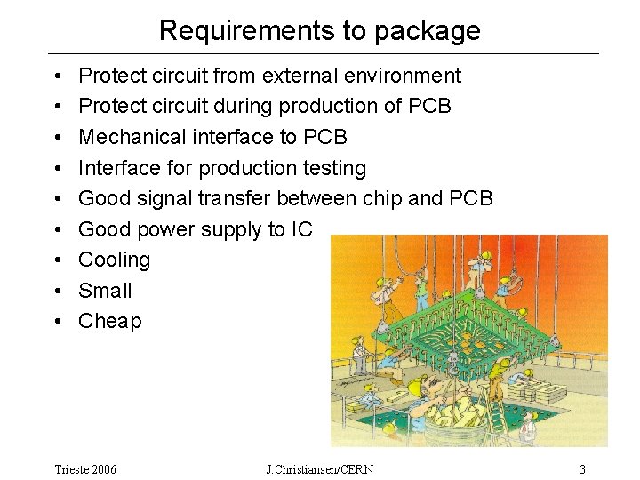
Requirements to package • • • Protect circuit from external environment Protect circuit during production of PCB Mechanical interface to PCB Interface for production testing Good signal transfer between chip and PCB Good power supply to IC Cooling Small Cheap Trieste 2006 J. Christiansen/CERN 3

Materials • Ceramic – Good heat conductivity – Hermetic – Expensive ( often more expensive than chip itself !) • Metal (has been used internally in IBM) – Good heat conductivity – Hermetic – Electrical conductive (must be mixed with other material) • Plastic – Cheap – Poor heat conductivity Can be improved by incorporating metallic heat plate. Trieste 2006 J. Christiansen/CERN 4

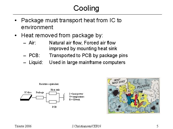
Cooling • Package must transport heat from IC to environment • Heat removed from package by: – Air: – PCB: – Liquid: Natural air flow, Forced air flow improved by mounting heat sink Transported to PCB by package pins Used in large mainframe computers Resistive equivalent IC dice Package Heat sink I = heat power V= temperature R = K/watt PCB Trieste 2006 J. Christiansen/CERN 5

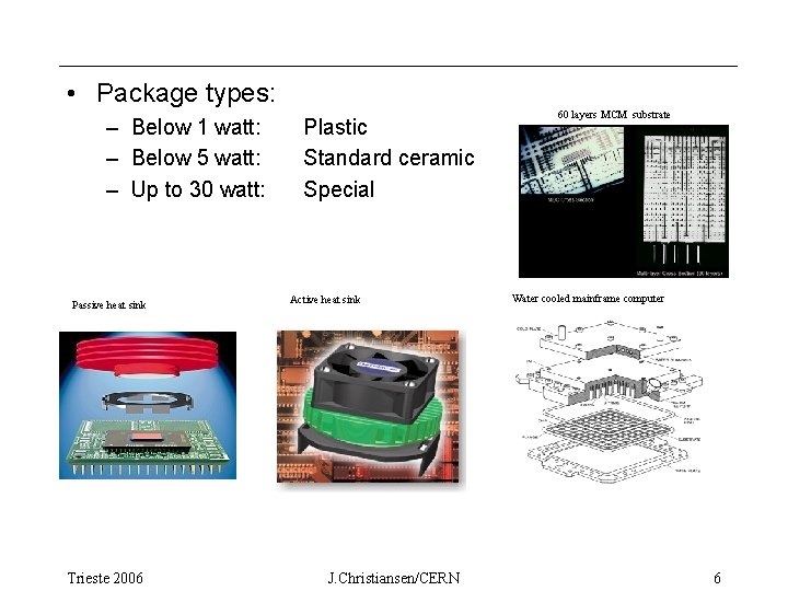
• Package types: – Below 1 watt: – Below 5 watt: – Up to 30 watt: Passive heat sink Trieste 2006 Plastic Standard ceramic Special Active heat sink J. Christiansen/CERN 60 layers MCM substrate Water cooled mainframe computer 6

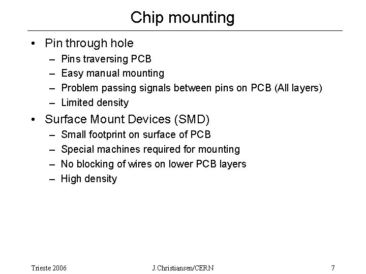
Chip mounting • Pin through hole – – Pins traversing PCB Easy manual mounting Problem passing signals between pins on PCB (All layers) Limited density • Surface Mount Devices (SMD) – – Small footprint on surface of PCB Special machines required for mounting No blocking of wires on lower PCB layers High density Trieste 2006 J. Christiansen/CERN 7

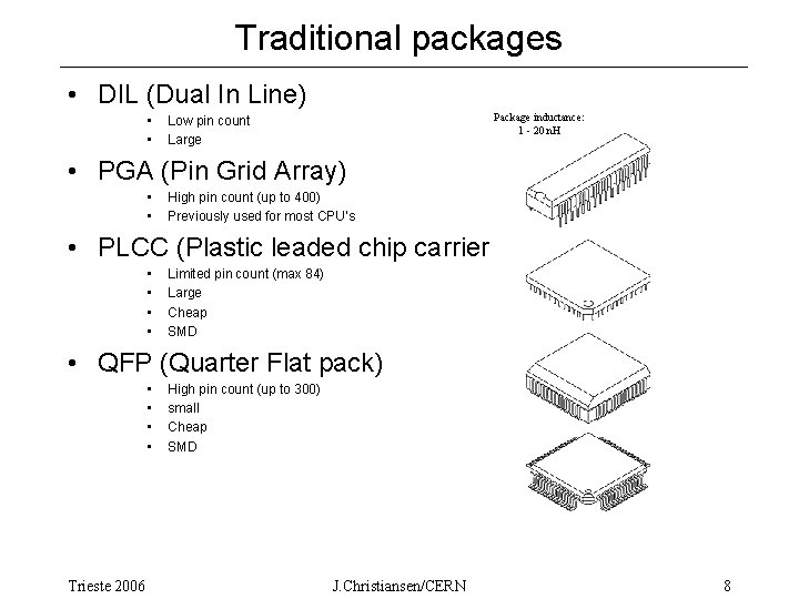
Traditional packages • DIL (Dual In Line) • • Package inductance: 1 - 20 n. H Low pin count Large • PGA (Pin Grid Array) • • High pin count (up to 400) Previously used for most CPU’s • PLCC (Plastic leaded chip carrier • • Limited pin count (max 84) Large Cheap SMD • QFP (Quarter Flat pack) • • Trieste 2006 High pin count (up to 300) small Cheap SMD J. Christiansen/CERN 8

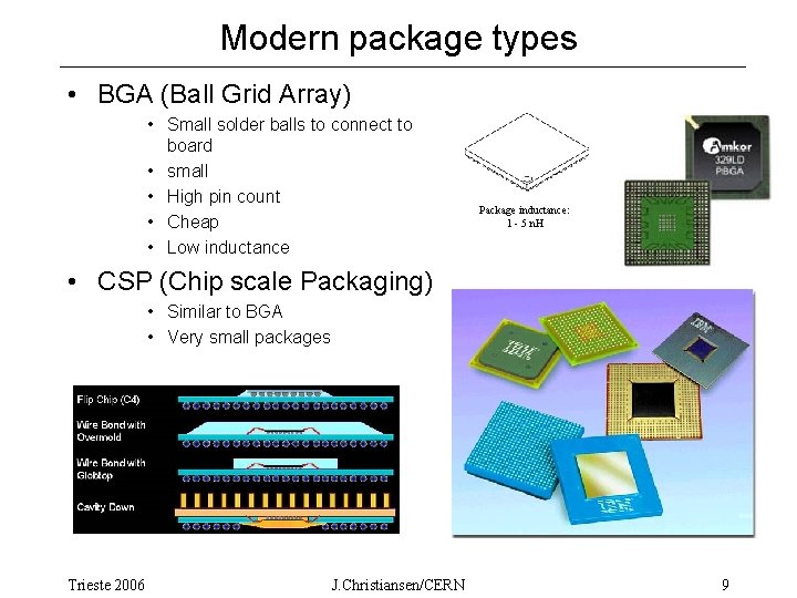
Modern package types • BGA (Ball Grid Array) • Small solder balls to connect to board • small • High pin count • Cheap • Low inductance Package inductance: 1 - 5 n. H • CSP (Chip scale Packaging) • Similar to BGA • Very small packages Trieste 2006 J. Christiansen/CERN 9

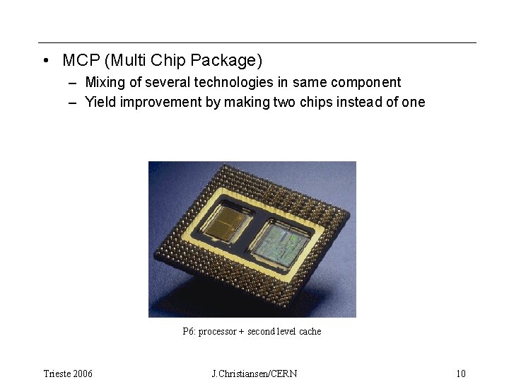
• MCP (Multi Chip Package) – Mixing of several technologies in same component – Yield improvement by making two chips instead of one P 6: processor + second level cache Trieste 2006 J. Christiansen/CERN 10

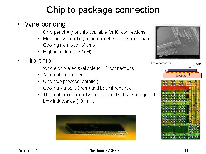
Chip to package connection • Wire bonding • • Only periphery of chip available for IO connections Mechanical bonding of one pin at a time (sequential) Cooling from back of chip High inductance (~1 n. H) • Flip-chip • • • Trieste 2006 Whole chip area available for IO connections Automatic alignment One step process (parallel) Cooling via balls (front) and back if required Thermal matching between chip and substrate required Low inductance (~0. 1 n. H) J. Christiansen/CERN 11

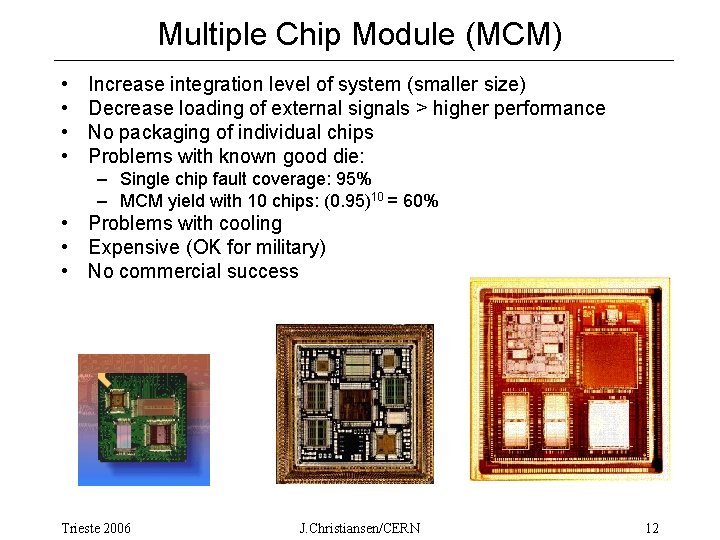
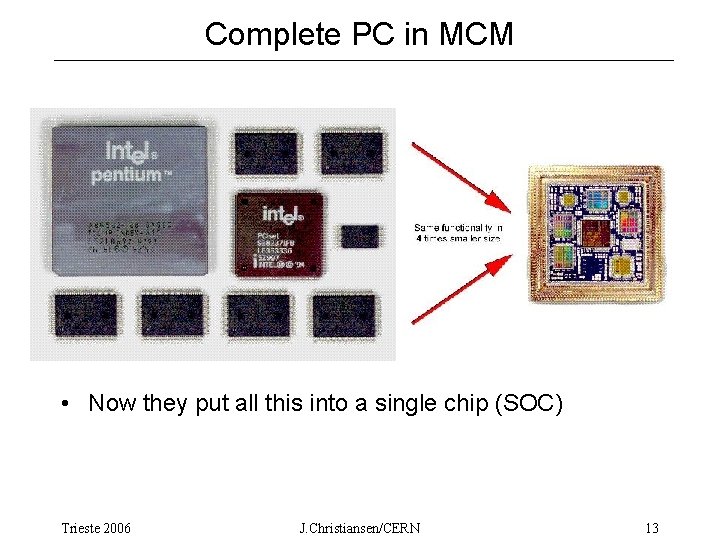
Multiple Chip Module (MCM) • • Increase integration level of system (smaller size) Decrease loading of external signals > higher performance No packaging of individual chips Problems with known good die: – Single chip fault coverage: 95% – MCM yield with 10 chips: (0. 95)10 = 60% • Problems with cooling • Expensive (OK for military) • No commercial success Trieste 2006 J. Christiansen/CERN 12

Complete PC in MCM • Now they put all this into a single chip (SOC) Trieste 2006 J. Christiansen/CERN 13

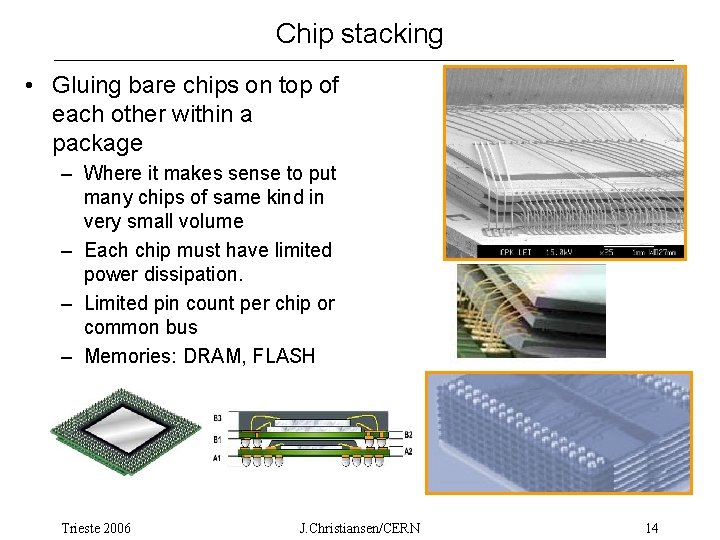
Chip stacking • Gluing bare chips on top of each other within a package – Where it makes sense to put many chips of same kind in very small volume – Each chip must have limited power dissipation. – Limited pin count per chip or common bus – Memories: DRAM, FLASH Trieste 2006 J. Christiansen/CERN 14

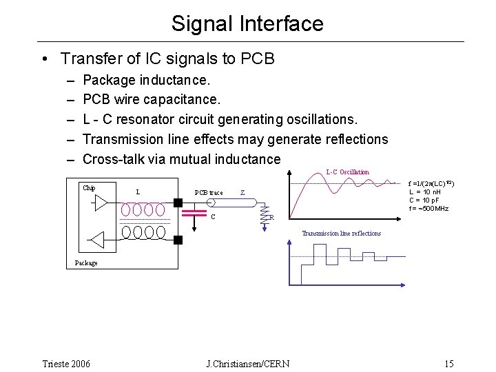
Signal Interface • Transfer of IC signals to PCB – – – Package inductance. PCB wire capacitance. L - C resonator circuit generating oscillations. Transmission line effects may generate reflections Cross-talk via mutual inductance L-C Oscillation Chip L PCB trace C f =1/(2 p(LC)1/2) L = 10 n. H C = 10 p. F f = ~500 MHz Z R Transmission line reflections Package Trieste 2006 J. Christiansen/CERN 15

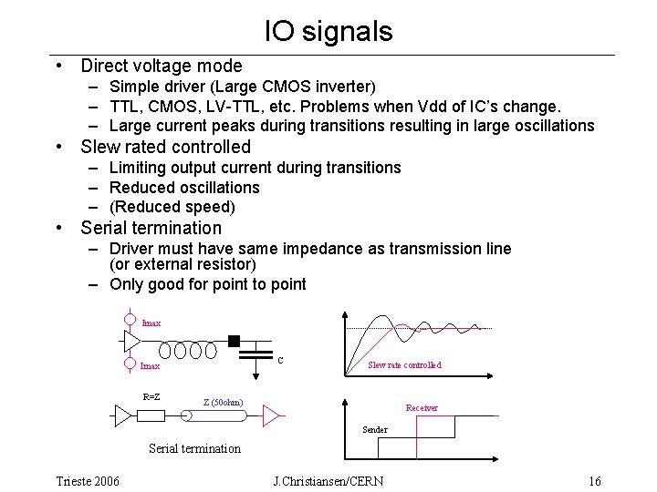
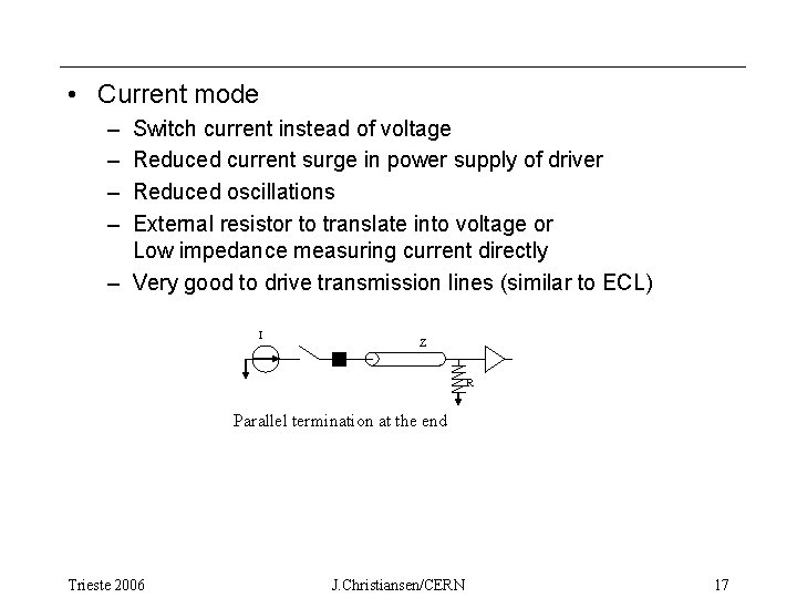
IO signals • Direct voltage mode – Simple driver (Large CMOS inverter) – TTL, CMOS, LV-TTL, etc. Problems when Vdd of IC’s change. – Large current peaks during transitions resulting in large oscillations • Slew rated controlled – Limiting output current during transitions – Reduced oscillations – (Reduced speed) • Serial termination – Driver must have same impedance as transmission line (or external resistor) – Only good for point to point Imax C Imax R=Z Slew rate controlled Z (50 ohm) Receiver Sender Serial termination Trieste 2006 J. Christiansen/CERN 16

• Current mode – – Switch current instead of voltage Reduced current surge in power supply of driver Reduced oscillations External resistor to translate into voltage or Low impedance measuring current directly – Very good to drive transmission lines (similar to ECL) I Z R Parallel termination at the end Trieste 2006 J. Christiansen/CERN 17

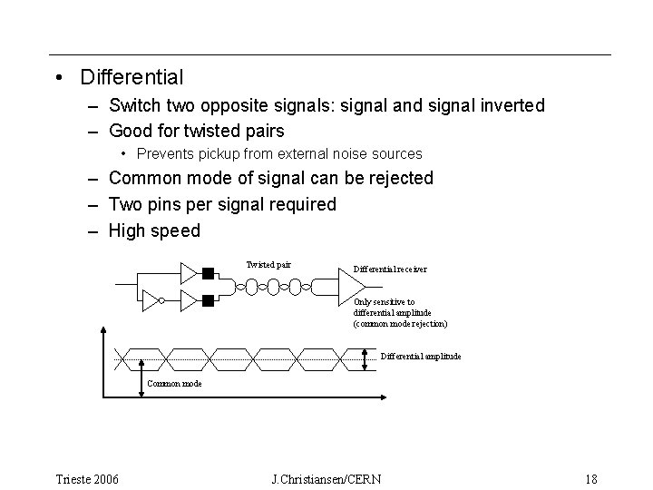
• Differential – Switch two opposite signals: signal and signal inverted – Good for twisted pairs • Prevents pickup from external noise sources – Common mode of signal can be rejected – Two pins per signal required – High speed Twisted pair Differential receiver Only sensitive to differential amplitude (common mode rejection) Differential amplitude Common mode Trieste 2006 J. Christiansen/CERN 18

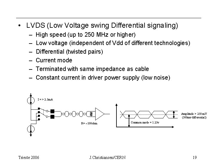
• LVDS (Low Voltage swing Differential signaling) – – – High speed (up to 250 MHz or higher) Low voltage (independent of Vdd of different technologies) Differential (twisted pairs) Current mode Terminated with same impedance as cable Constant current in driver power supply (low noise) I = > 2. 5 m. A Amplitude > 250 m. V (500 mv differential) R= ~100 ohm Trieste 2006 J. Christiansen/CERN Common mode = 1. 25 v 19

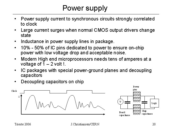
Power supply • Power supply current to synchronous circuits strongly correlated to clock • Large current surges when normal CMOS output drivers change state • Inductance in power supply lines in package. • 10% - 50% of IC pins dedicated to power to ensure on-chip power with low voltage drop and acceptable noise. • Modern High end microprocessors needs tens of amperes at a voltage of 1 – 2 volt !. • IC packages with special power-ground planes and decoupling capacitors • Decoupling capacitors on chip Power pins Clock I V Board capacitance Trieste 2006 J. Christiansen/CERN Logic Chip capacitance 20

Testing: Cost of finding failing chip Trieste 2006 J. Christiansen/CERN 21

Design verification testing Trieste 2006 J. Christiansen/CERN 22

Production testing Trieste 2006 J. Christiansen/CERN 23

Production yield Trieste 2006 J. Christiansen/CERN 24

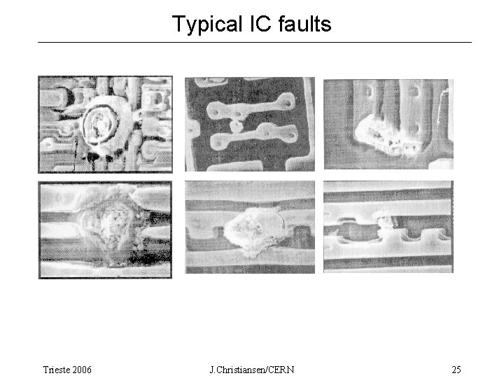
Typical IC faults Trieste 2006 J. Christiansen/CERN 25

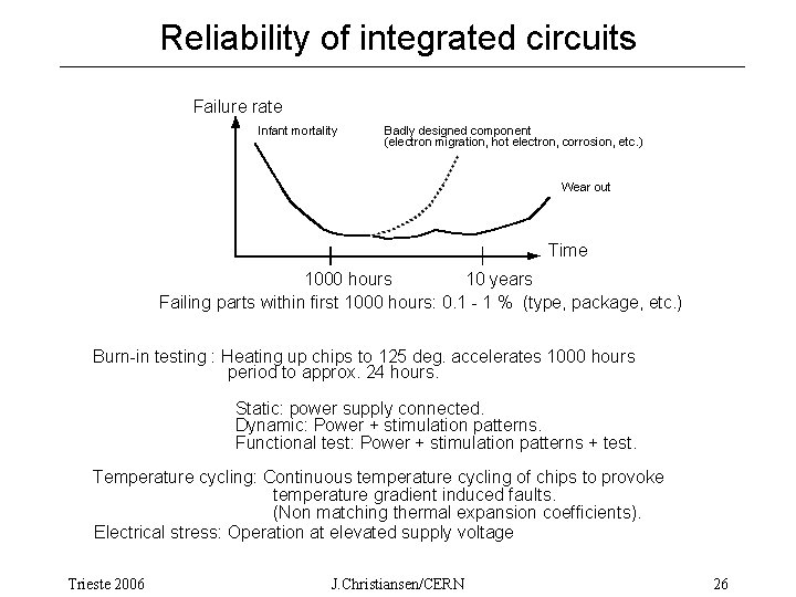
Reliability of integrated circuits Failure rate Infant mortality Badly designed component (electron migration, hot electron, corrosion, etc. ) Wear out Time 1000 hours 10 years Failing parts within first 1000 hours: 0. 1 - 1 % (type, package, etc. ) Burn-in testing : Heating up chips to 125 deg. accelerates 1000 hours period to approx. 24 hours. Static: power supply connected. Dynamic: Power + stimulation patterns. Functional test: Power + stimulation patterns + test. Temperature cycling: Continuous temperature cycling of chips to provoke temperature gradient induced faults. (Non matching thermal expansion coefficients). Electrical stress: Operation at elevated supply voltage Trieste 2006 J. Christiansen/CERN 26

What to test Trieste 2006 J. Christiansen/CERN 27

Basic testing terms Trieste 2006 J. Christiansen/CERN 28

Fault models Trieste 2006 J. Christiansen/CERN 29

Problematic faults at transistor level Trieste 2006 J. Christiansen/CERN 30

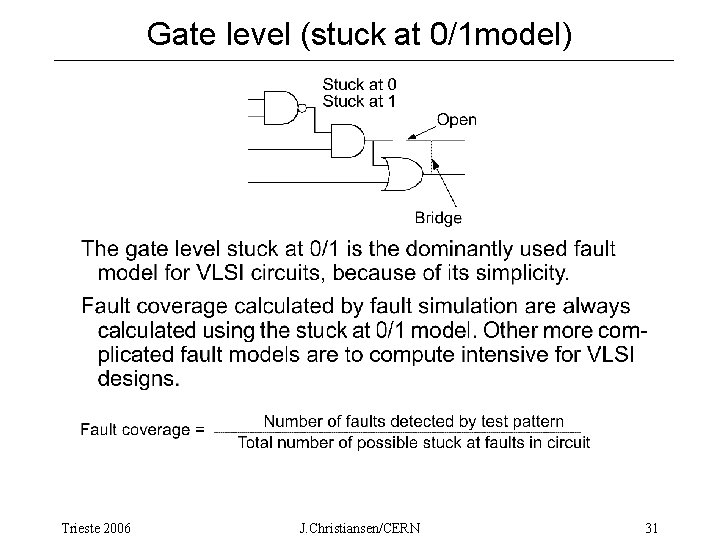
Gate level (stuck at 0/1 model) Trieste 2006 J. Christiansen/CERN 31

Testability Trieste 2006 J. Christiansen/CERN 32

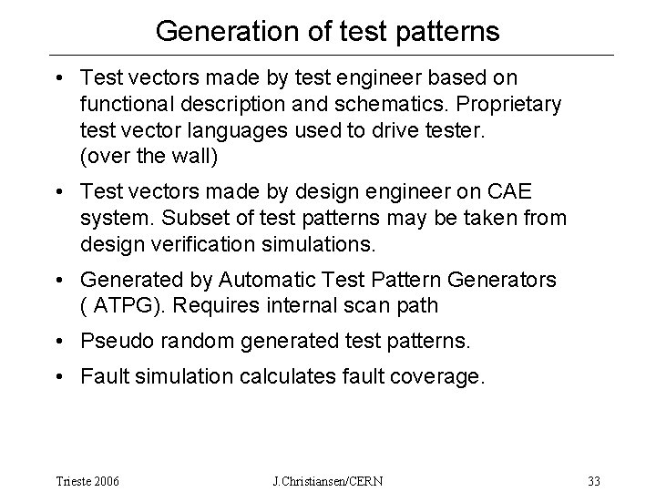
Generation of test patterns • Test vectors made by test engineer based on functional description and schematics. Proprietary test vector languages used to drive tester. (over the wall) • Test vectors made by design engineer on CAE system. Subset of test patterns may be taken from design verification simulations. • Generated by Automatic Test Pattern Generators ( ATPG). Requires internal scan path • Pseudo random generated test patterns. • Fault simulation calculates fault coverage. Trieste 2006 J. Christiansen/CERN 33

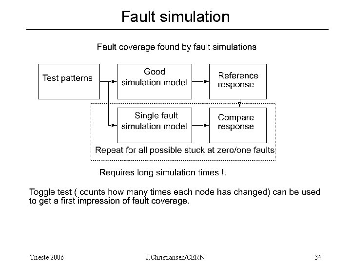
Fault simulation Trieste 2006 J. Christiansen/CERN 34

Test development with increased complexity Trieste 2006 J. Christiansen/CERN 35

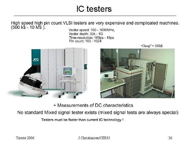
IC testers “Cheap” = Trieste 2006 J. Christiansen/CERN 500 k$ 36

Scan Path testing Trieste 2006 J. Christiansen/CERN 37

Scan path testing Trieste 2006 J. Christiansen/CERN 38

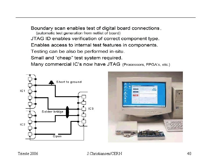
JTAG standard Trieste 2006 J. Christiansen/CERN 39

Trieste 2006 J. Christiansen/CERN 40

Built In Self Test (BIST) All commercial high end IC have extensive built in test features, but they are not documented for normal users as they do not need to know for normal use and it is a part of the “secrets” of how to produce high quality ICs Trieste 2006 J. Christiansen/CERN 41

Good design practices (If time allows) J. Christiansen/CERN

Purpose of good design practices • • Improve chance of chip working first time Reduce (total) design time Reduce development cost Improved reliability Improved production yield. Follow vendor rules to get standard guarantees. Some performance reduction may have to be accepted • (Be smart but not to smart) Trieste 2006 J. Christiansen/CERN 43

Choice of technology • Performance (speed, complexity) • Design tools : Synthesis, P&R, etc. – Cost of required tools – Support for tools from which CAE tool supplier • Libraries (gates, adders, RAM, ROM, PLL’s, PCI, ADC, etc. ) • Development costs – Full engineering run: NRE (several hundred thousand dollars) – Multi Project Wafer (MPW) • Life time of technology – Modern CMOS only have a life time of ~5 years • Production – Price as function of volume – Production testing Trieste 2006 J. Christiansen/CERN 44

Well planned design hierarchy • The hierarchy of a design is the base for the whole design process. – Define logical functional blocks – Minimize connections between branches of hierarchy – Keep in mind that Hierarchy is going to be used for synthesis, simulation, Place & route, testing, etc. • Define architecture in a top-down approach • Evaluate implementation and performance of critical blocks to determine if architecture must be changed. Trieste 2006 J. Christiansen/CERN 45

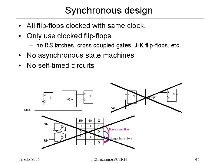
Synchronous design • All flip-flops clocked with same clock. • Only use clocked flip-flops – no RS latches, cross coupled gates, J-K flip-flops, etc. • No asynchronous state machines • No self-timed circuits d d q Logic Clock Sb Rb Trieste 2006 d q Q Rb Sb Q 0 0 1 0 1 1 1 Q* Race condition Legal transitions J. Christiansen/CERN 46

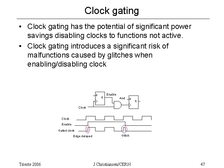
Clock gating • Clock gating has the potential of significant power savings disabling clocks to functions not active. • Clock gating introduces a significant risk of malfunctions caused by glitches when enabling/disabling clock d q Enable And d q Clock Enable Gated clock Edge delayed Trieste 2006 Glitch J. Christiansen/CERN 47

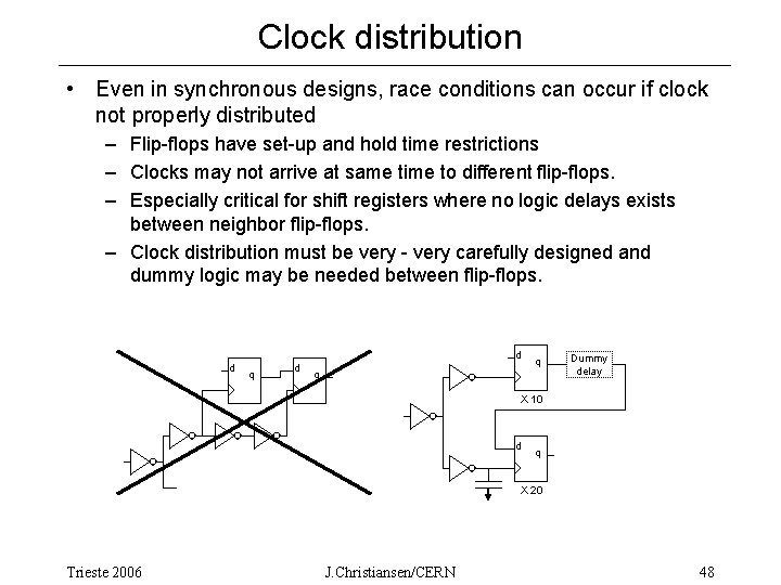
Clock distribution • Even in synchronous designs, race conditions can occur if clock not properly distributed – Flip-flops have set-up and hold time restrictions – Clocks may not arrive at same time to different flip-flops. – Especially critical for shift registers where no logic delays exists between neighbor flip-flops. – Clock distribution must be very - very carefully designed and dummy logic may be needed between flip-flops. d d q q Dummy delay X 10 d q X 20 Trieste 2006 J. Christiansen/CERN 48

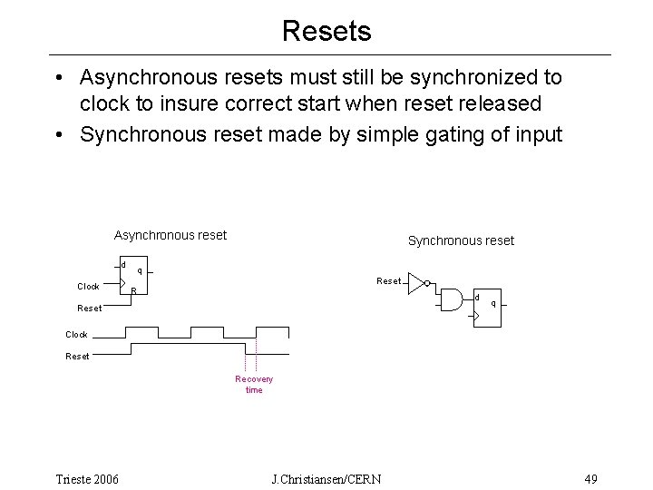
Resets • Asynchronous resets must still be synchronized to clock to insure correct start when reset released • Synchronous reset made by simple gating of input Asynchronous reset d Clock Synchronous reset q Reset R d Reset q Clock Reset Recovery time Trieste 2006 J. Christiansen/CERN 49

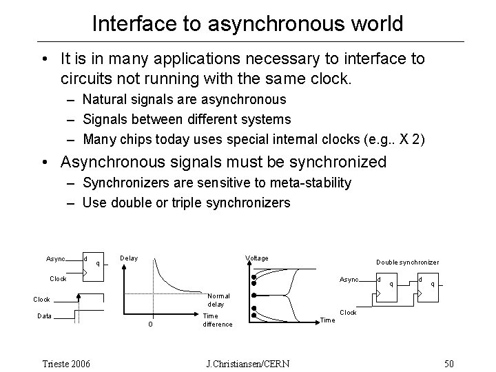
Interface to asynchronous world • It is in many applications necessary to interface to circuits not running with the same clock. – Natural signals are asynchronous – Signals between different systems – Many chips today uses special internal clocks (e. g. . X 2) • Asynchronous signals must be synchronized – Synchronizers are sensitive to meta-stability – Use double or triple synchronizers Async. d q Delay Voltage Double synchronizer Clock Async. q d q Normal delay Clock Data 0 Trieste 2006 d Time difference J. Christiansen/CERN Time Clock 50

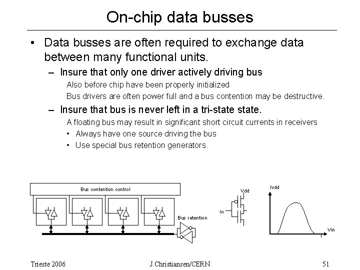
On-chip data busses • Data busses are often required to exchange data between many functional units. – Insure that only one driver actively driving bus Also before chip have been properly initialized Bus drivers are often power full and a bus contention may be destructive. – Insure that bus is never left in a tri-state. A floating bus may result in significant short circuit currents in receivers • Always have one source driving the bus • Use special bus retention generators. Bus contention control Vdd Ivdd In Bus retention Vin Trieste 2006 J. Christiansen/CERN 51

Mixed signal designs • Extreme care must be taken in mixed analog - digital integrated circuits to limit coupling to the sensitive analog part. – Separate power supplies for analog and digital • Best powering scheme for sensitive mixed signal designs depends strongly on used technology: – High conductive substrate – Low conductive substrate – Silicon on Insulator (SOI) – Guard ring connected to ground analog blocks Efficiency of this depends a lot on substrate type. – Separate test of analog and digital (scan path) – Use differential analog circuits to reject common mode noise • If not using differential analog one is most likely in trouble – Be careful with digital outputs which may inject noise into analog part (use if possible differential outputs) • Difficult but can be done Trieste 2006 J. Christiansen/CERN 52

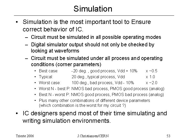
Simulation • Simulation is the most important tool to Ensure correct behavior of IC. – Circuit must be simulated in all possible operating modes – Digital simulator output should not only be checked by looking at waveforms – Circuit must be simulated under all process and operating conditions (corner parameters) • • • Best case: -20 deg. , good process, Vdd + 10% x ~0. 5 Typical: 20 deg. , typical process, Vdd x 1. 0 Worst case: 100 deg. , bad process, Vdd - 10% x ~2. 0 Worst N - best P: NMOS bad process, PMOS good process (analog) Best N - worst P: NMOS good process, PMOS bad process (analog) Plus many other combinations of different device parameters (which combination is the worst for my circuit ? ) • IC designers spend most of their time simulating and writing simulation environments. Trieste 2006 J. Christiansen/CERN 53

Testing • One can “never” put to much test facilities in chips. • Put scan path where ever possible. • Have special test outputs which can be used for monitoring of critical circuits. • Put internal test pads on special tricky analog circuits. • If in doubt about critical parameters of design make it programmable if possible. • Do not forget about production testing. • Do not make a redesign before problems with current version well understood. • Most designs needs some kind of redesign. Trieste 2006 J. Christiansen/CERN 54

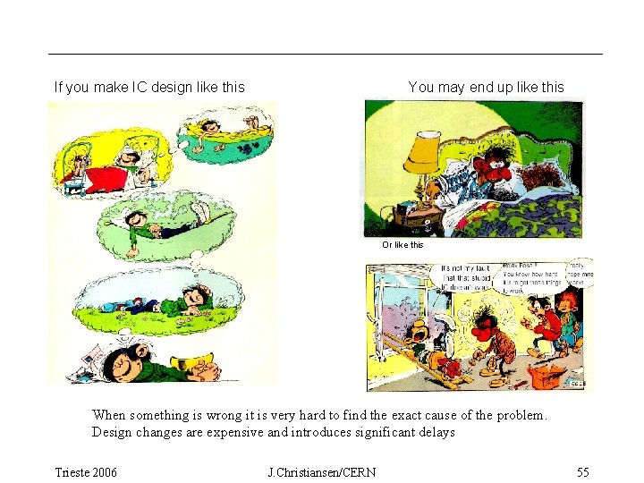
If you make IC design like this You may end up like this Or like this When something is wrong it is very hard to find the exact cause of the problem. Design changes are expensive and introduces significant delays Trieste 2006 J. Christiansen/CERN 55