IC packaging and Input output signals J Christiansen
- Slides: 24

IC packaging and Input - output signals J. Christiansen, CERN - EP/MIC Jorgen. Christiansen@cern. ch J. Christiansen/CERN

Requirements to package • • • Protect circuit from external environment Protect circuit during production of PCB Mechanical interface to PCB Interface for production testing Good signal transfer between chip and PCB Good power supply to IC Cooling Small Cheap December 2003 J. Christiansen/CERN 2

Materials • Ceramic – Good heat conductivity – Hermetic – Expensive ( often more expensive than chip itself !) • Metal (has been used internally in IBM) – Good heat conductivity – Hermetic – Electrical conductive (must be mixed with other material) • Plastic – Cheap – Poor heat conductivity Can be improved by incorporating metallic heat plate. December 2003 J. Christiansen/CERN 3

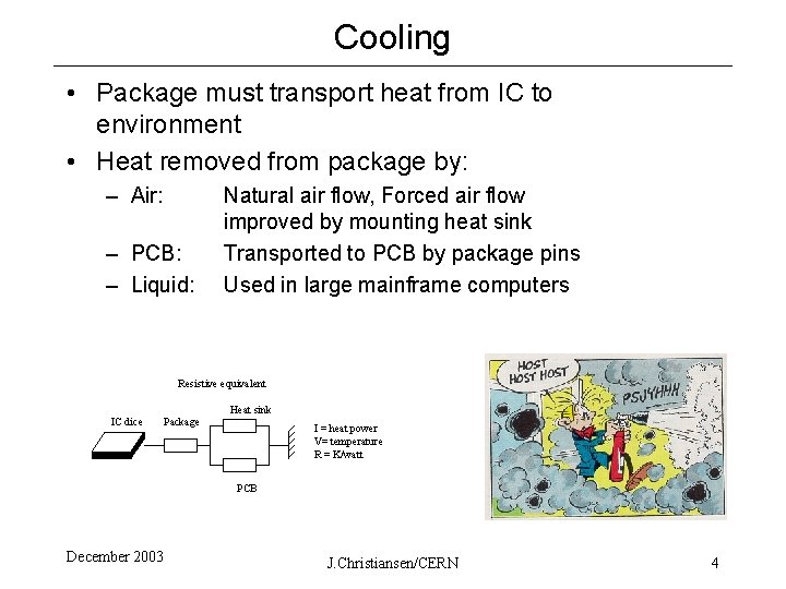
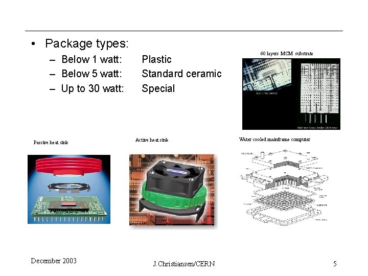
Cooling • Package must transport heat from IC to environment • Heat removed from package by: – Air: – PCB: – Liquid: Natural air flow, Forced air flow improved by mounting heat sink Transported to PCB by package pins Used in large mainframe computers Resistive equivalent IC dice Package Heat sink I = heat power V= temperature R = K/watt PCB December 2003 J. Christiansen/CERN 4

• Package types: – Below 1 watt: – Below 5 watt: – Up to 30 watt: Passive heat sink December 2003 Plastic Standard ceramic Special Active heat sink J. Christiansen/CERN 60 layers MCM substrate Water cooled mainframe computer 5

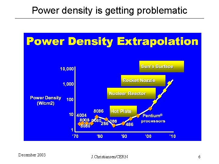
Power density is getting problematic December 2003 J. Christiansen/CERN 6

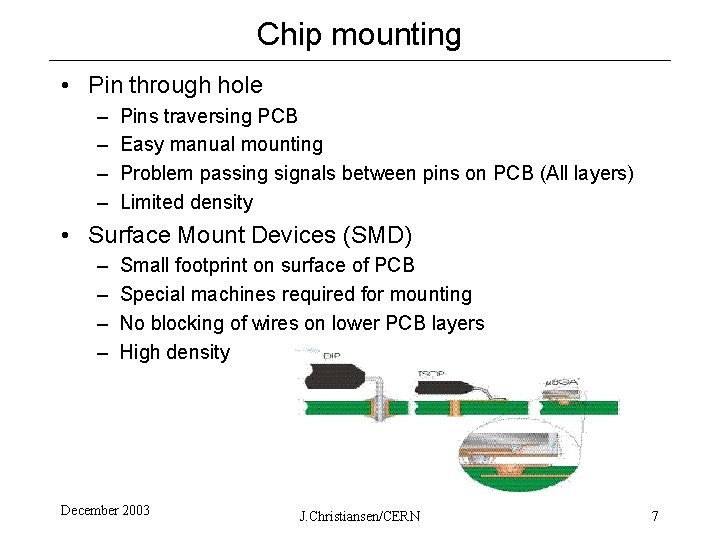
Chip mounting • Pin through hole – – Pins traversing PCB Easy manual mounting Problem passing signals between pins on PCB (All layers) Limited density • Surface Mount Devices (SMD) – – Small footprint on surface of PCB Special machines required for mounting No blocking of wires on lower PCB layers High density December 2003 J. Christiansen/CERN 7

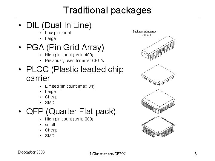
Traditional packages • DIL (Dual In Line) Package inductance: 1 - 20 n. H • Low pin count • Large • PGA (Pin Grid Array) • High pin count (up to 400) • Previously used for most CPU’s • PLCC (Plastic leaded chip carrier • • Limited pin count (max 84) Large Cheap SMD • QFP (Quarter Flat pack) • • December 2003 High pin count (up to 300) small Cheap SMD J. Christiansen/CERN 8

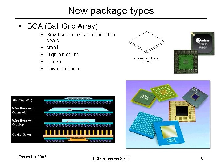
New package types • BGA (Ball Grid Array) • Small solder balls to connect to board • small • High pin count • Cheap • Low inductance December 2003 J. Christiansen/CERN Package inductance: 1 - 5 n. H 9

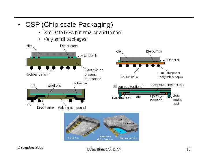
• CSP (Chip scale Packaging) • Similar to BGA but smaller and thinner • Very small packages December 2003 J. Christiansen/CERN 10

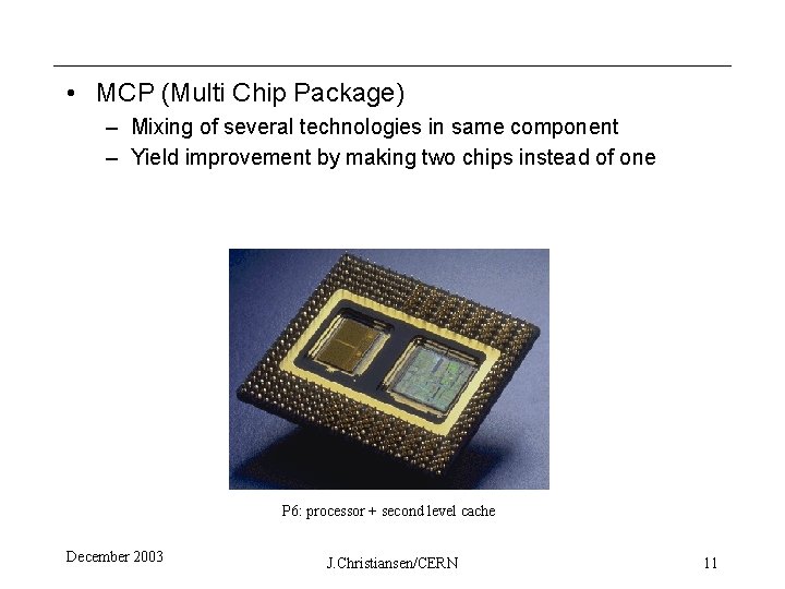
• MCP (Multi Chip Package) – Mixing of several technologies in same component – Yield improvement by making two chips instead of one P 6: processor + second level cache December 2003 J. Christiansen/CERN 11

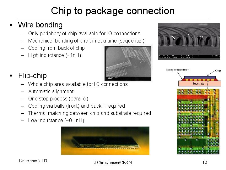
Chip to package connection • Wire bonding – – Only periphery of chip available for IO connections Mechanical bonding of one pin at a time (sequential) Cooling from back of chip High inductance (~1 n. H) • Flip-chip – – – Whole chip area available for IO connections Automatic alignment One step process (parallel) Cooling via balls (front) and back if required Thermal matching between chip and substrate required Low inductance (~0. 1 n. H) December 2003 J. Christiansen/CERN 12

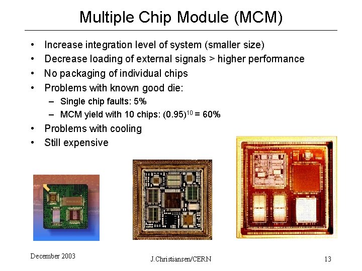
Multiple Chip Module (MCM) • • Increase integration level of system (smaller size) Decrease loading of external signals > higher performance No packaging of individual chips Problems with known good die: – Single chip faults: 5% – MCM yield with 10 chips: (0. 95)10 = 60% • Problems with cooling • Still expensive December 2003 J. Christiansen/CERN 13

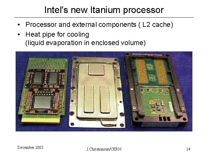
Intel's new Itanium processor • Processor and external components ( L 2 cache) • Heat pipe for cooling (liquid evaporation in enclosed volume) December 2003 J. Christiansen/CERN 14

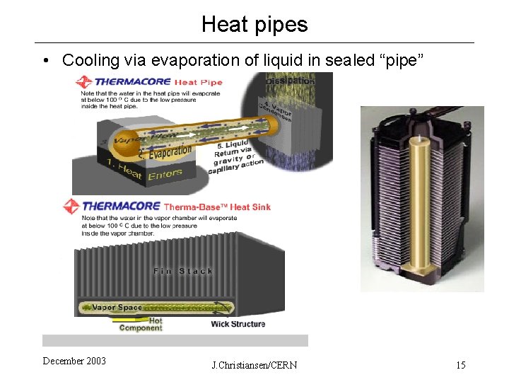
Heat pipes • Cooling via evaporation of liquid in sealed “pipe” December 2003 J. Christiansen/CERN 15

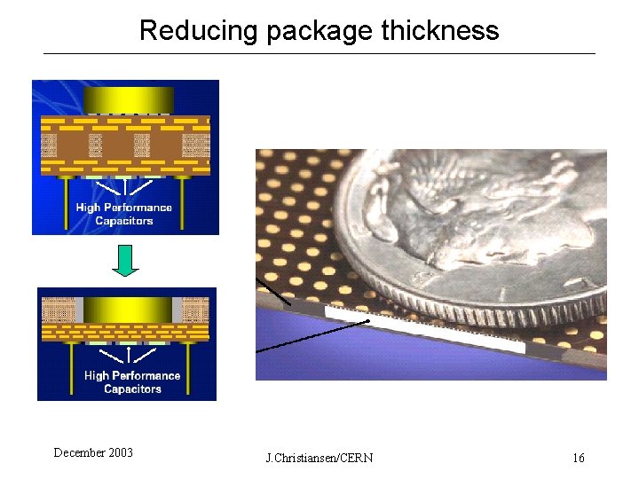
Reducing package thickness December 2003 J. Christiansen/CERN 16

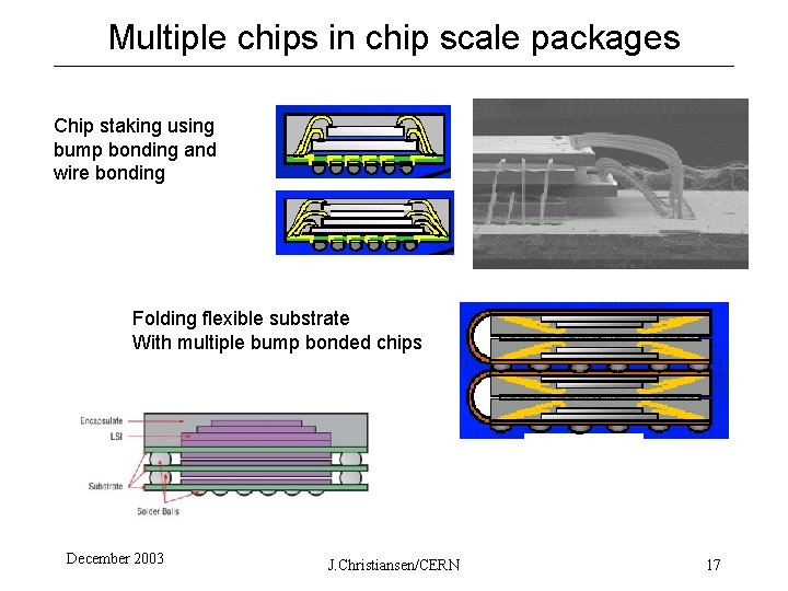
Multiple chips in chip scale packages Chip staking using bump bonding and wire bonding Folding flexible substrate With multiple bump bonded chips December 2003 J. Christiansen/CERN 17

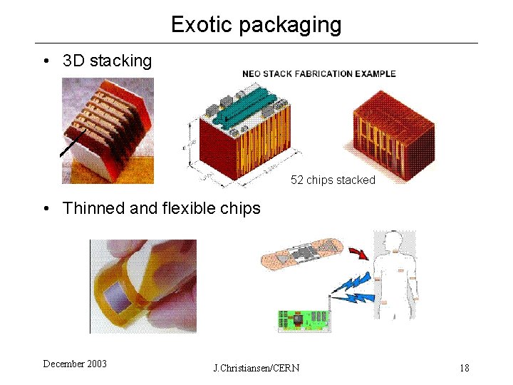
Exotic packaging • 3 D stacking 52 chips stacked • Thinned and flexible chips December 2003 J. Christiansen/CERN 18

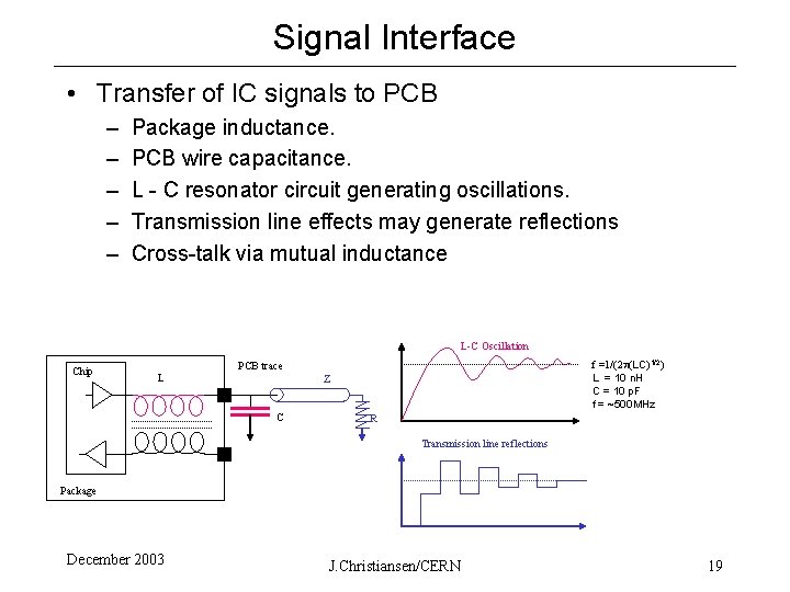
Signal Interface • Transfer of IC signals to PCB – – – Package inductance. PCB wire capacitance. L - C resonator circuit generating oscillations. Transmission line effects may generate reflections Cross-talk via mutual inductance L-C Oscillation Chip L f =1/(2 p(LC)1/2) L = 10 n. H C = 10 p. F f = ~500 MHz PCB trace Z C R Transmission line reflections Package December 2003 J. Christiansen/CERN 19

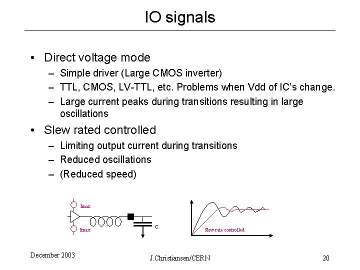
IO signals • Direct voltage mode – Simple driver (Large CMOS inverter) – TTL, CMOS, LV-TTL, etc. Problems when Vdd of IC’s change. – Large current peaks during transitions resulting in large oscillations • Slew rated controlled – Limiting output current during transitions – Reduced oscillations – (Reduced speed) Imax December 2003 C Slew rate controlled J. Christiansen/CERN 20

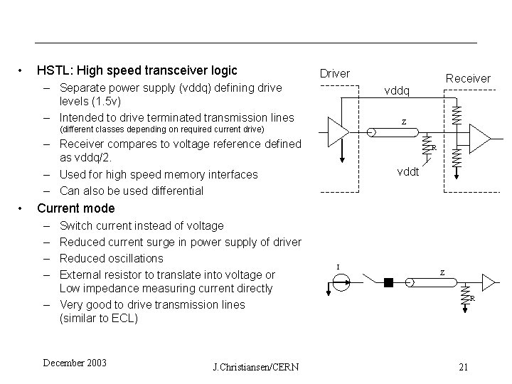
• HSTL: High speed transceiver logic Driver – Separate power supply (vddq) defining drive levels (1. 5 v) – Intended to drive terminated transmission lines vddq Z (different classes depending on required current drive) – Receiver compares to voltage reference defined as vddq/2. – Used for high speed memory interfaces – Can also be used differential • Receiver R vddt Current mode – – Switch current instead of voltage Reduced current surge in power supply of driver Reduced oscillations External resistor to translate into voltage or Low impedance measuring current directly – Very good to drive transmission lines (similar to ECL) December 2003 J. Christiansen/CERN I Z R 21

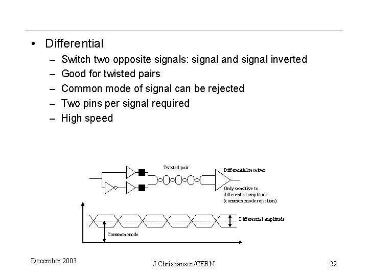
• Differential – – – Switch two opposite signals: signal and signal inverted Good for twisted pairs Common mode of signal can be rejected Two pins per signal required High speed Twisted pair Differential receiver Only sensitive to differential amplitude (common mode rejection) Differential amplitude Common mode December 2003 J. Christiansen/CERN 22

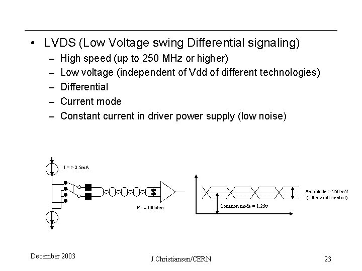
• LVDS (Low Voltage swing Differential signaling) – – – High speed (up to 250 MHz or higher) Low voltage (independent of Vdd of different technologies) Differential Current mode Constant current in driver power supply (low noise) I = > 2. 5 m. A Amplitude > 250 m. V (500 mv differential) R= ~100 ohm December 2003 J. Christiansen/CERN Common mode = 1. 25 v 23

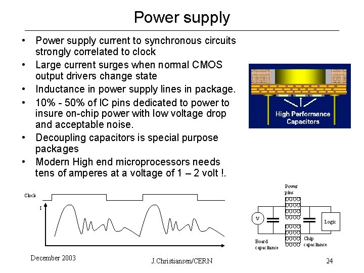
Power supply • Power supply current to synchronous circuits strongly correlated to clock • Large current surges when normal CMOS output drivers change state • Inductance in power supply lines in package. • 10% - 50% of IC pins dedicated to power to insure on-chip power with low voltage drop and acceptable noise. • Decoupling capacitors is special purpose packages • Modern High end microprocessors needs tens of amperes at a voltage of 1 – 2 volt !. Power pins Clock I V Board capacitance December 2003 J. Christiansen/CERN Logic Chip capacitance 24