Lesson 4 The physics of lowdimensional semiconductors A

 Basic properties of 2 D semiconductor nanostructures Quantum well for electrons Heterostructure Thin")
 Al. Ga. As - Interband processes - Intraband processes E(z) engineering (modulation)")

")


 Parabolic and triangular quantum wells - Parabolic well")


 Superlattices")


 Modulation-doped heterojunctions")
 MOSFET structures 2 D Electron Gas")
 Quantum wires (1 D semiconductor nanostructures) C Nanotubes Si, Ge nanowires")
 A new band diagram (modified by the")

 Quantum dots (0 D semiconductor nanostructures)")

 EC (e 2/C) and single electron effects")


- Slides: 33
Lesson 4: The physics of low-dimensional semiconductors
A) Basic properties of 2 D semiconductor nanostructures Quantum well for electrons Heterostructure Thin film of a pure or composed material Common physics
Heterostructure (MBE) Al. Ga. As - Interband processes - Intraband processes E(z) engineering (modulation) a) Band Engineering b) Thickness Engineering
Superlattice Electronic transport? ? ?
Electric Field Applied Or Magnetic Field Applied V Electronic transport occurs determined by: A) A new band diagram (modified by the electric or magnetic field) B) Electronic density of states C) Tunnelling phenomena D) Temperature E) Electroniuc coupling F) Scattering phenomena
k. T a<<le k. T<<ΔE
Interband Transitions
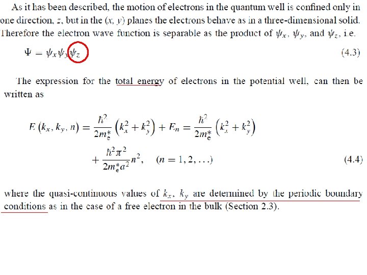
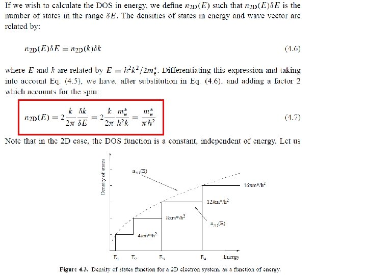
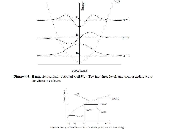
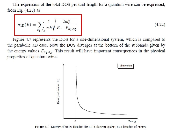
Density of electronic states in a quantum well 3 D 2 D
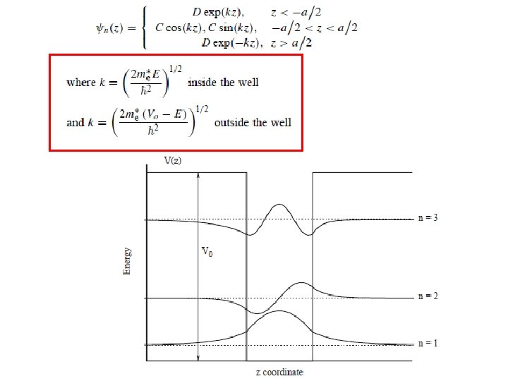
A 1) Parabolic and triangular quantum wells - Parabolic well
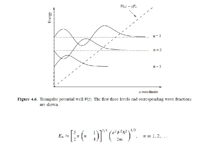
- Triangular well
V
V=0 V 0
A. 2) Superlattices
- Kronig-Penney model of a superlattices
Minigaps Minibands
A 3) Modulation-doped heterojunctions
A 4) MOSFET structures 2 D Electron Gas
B) Quantum wires (1 D semiconductor nanostructures) C Nanotubes Si, Ge nanowires
V Electronic transport occurs determined by: A) A new band diagram (modified by the electric or magnetic field) B) Electronic density of states C) Tunnelling phenomena D) Temperature E) Electroniuc coupling F) Scattering phenomena
Density of electronic states in a quantum wire
C) Quantum dots (0 D semiconductor nanostructures)
Current? ? ?
Charging energy (ionization energy) EC (e 2/C) and single electron effects
ΔE EC k. T 3 D: ΔE>>EC 2 D: ΔE>>EC 1 D: ΔE>>EC 0 D: ΔE~EC 3 D, 2 D, 1 D ΔE EC k. T 0 D EC ΔE k. T
Density of electronic states in a quantum dots