
Chapter 3 Semiconductors from Microelectronic Circuits Text by
Chapter #3: Semiconductors from Microelectronic Circuits Text by Sedra and Smith Oxford Publishing Oxford University Publishing Microelectronic Circuits by Adel S. Sedra and Kenneth C. Smith (0195323033)
Introduction § IN THIS CHAPTER WE WILL LEARN: § The basic properties of semiconductors and, in particular, silicone – the material used to make most modern electronic circuits. § How doping a pure silicon crystal dramatically changes its electrical conductivity – the fundamental idea in underlying the use of semiconductors in the implementation of electronic devices. Oxford University Publishing Microelectronic Circuits by Adel S. Sedra and Kenneth C. Smith (0195323033)
Introduction § IN THIS CHAPTER WE WILL LEARN: § The two mechanisms by which current flows in semiconductors – drift and diffusion charge carriers. § The structure and operation of the pn junction – a basic semiconductor structure that implements the diode and plays a dominant role in semiconductors. Oxford University Publishing Microelectronic Circuits by Adel S. Sedra and Kenneth C. Smith (0195323033)
3. 1. Intrinsic Semiconductors § semiconductor – a material whose conductivity lies between that of conductors (copper) and insulators (glass). § single-element – such as germanium and silicon. § compound – such as gallium-arsenide. Oxford University Publishing Microelectronic Circuits by Adel S. Sedra and Kenneth C. Smith (0195323033)
3. 1. Intrinsic Semiconductors § valence electron – is an electron that participates in the formation of chemical bonds. § Atoms with one or two valence electrons more than a closed shell are highly reactive because the extra electrons are easily removed to form positive ions. § covalent bond – is a form of chemical bond in which two atoms share a pair of atoms. § It is a stable balance of attractive and repulsive forces between atoms when they share electrons. Oxford University Publishing Microelectronic Circuits by Adel S. Sedra and Kenneth C. Smith (0195323033)

3. 1. Intrinsic Semiconductors § silicon atom § four valence electrons § requires four more to complete outermost shell § each pair of shared forms a covalent bond § the atoms form a lattice structure Oxford University Publishing Microelectronic Circuits by Adel S. Sedra and Kenneth C. Smith (0195323033) Figure 3. 1 Two-dimensional representation of the silicon crystal. The circles represent the inner core of silicon atoms, with +4 indicating its positive charge of +4 q, which is neutralized by the charge of the four valence electrons. Observe how the covalent bonds are formed by sharing of the valence electrons. At 0 K, all bonds are intact and no free electrons are available for current conduction.
3. 1. of. Intrinsic The process freeing electrons, creating holes, and filling them facilitates current flow… Semiconductors § silicon at low temps § all covalent bonds – are intact § no electrons – are available for conduction § conducitivity – is zero § silicon at room temp § some covalent bonds – break, freeing an electron and creating hole, due to thermal energy § some electrons – will wander from their parent atoms, becoming available for conduction § conductivity – is greater than zero Oxford University Publishing Microelectronic Circuits by Adel S. Sedra and Kenneth C. Smith (0195323033)
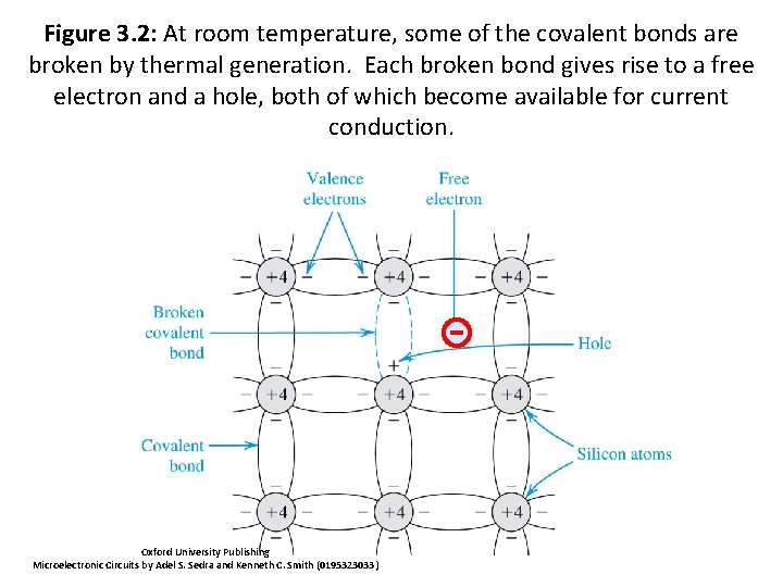
Figure 3. 2: At room temperature, some of the covalent bonds are 3. 1: Intrinsic broken by thermal generation. Each broken bond gives rise to a free Semiconductors electron and a hole, both of which become available for current conduction. § silicon at low temps: § all covalent bonds are intact § no electrons are available for conduction § conducitivity is zero the process of and filling § silicon at room temp: § sufficient thermal energy exists to break some covalent bonds, freeing an electron and creating hole § a free electron may wander freeing electrons, creating from its parent atomholes, § a hole will attract neighboring them facilitates current flow electrons Oxford University Publishing Microelectronic Circuits by Adel S. Sedra and Kenneth C. Smith (0195323033)
3. 1. Intrinsic Semiconductors § intrinsic semiconductor – is one which is not doped § One example is pure silicon. § generation – is the process of free electrons and holes being created. § generation rate – is speed with which this occurs. § recombination – is the process of free electrons and holes disappearing. § recombination – is speed with which this. Asoccurs. Generation may be rate effected by thermal energy. such, both generation and recombination rates will be (at least in part) a function of temperature. Oxford University Publishing Microelectronic Circuits by Adel S. Sedra and Kenneth C. Smith (0195323033)
3. 1. Intrinsic Semiconductors § thermal generation – effects a equal concentration of free electrons and holes. § Therefore, electrons move randomly throughout the material. § In thermal equilibrium, generation and recombination rates are equal. Oxford University Publishing Microelectronic Circuits by Adel S. Sedra and Kenneth C. Smith (0195323033)
3. 1. Intrinsic Semiconductors § In thermal equilibrium, the behavior below applies… § ni = number of free electrons and holes / unit volume § p = number of holes § n = number of free electrons Oxford University Publishing Microelectronic Circuits by Adel S. Sedra and Kenneth C. Smith (0195323033)
3. 1. Intrinsic Semiconductors § ni = number of free electrons and holes in a unit volume for intrinsic semiconductor § B = parameter which is 7. 3 E 15 cm-3 K-3/2 for silicon § T = temperature (K) § Eg = bandgap energy which is 1. 12 e. V for silicon § k = Boltzman constant (8. 62 E-5 e. V/K) Oxford University Publishing Microelectronic Circuits by Adel S. Sedra and Kenneth C. Smith (0195323033)
Example 3. 1 § Refer to book… Oxford University Publishing Microelectronic Circuits by Adel S. Sedra and Kenneth C. Smith (0195323033)
3. 1. Intrinsic Semiconductors § Q: Why can thermal generation not be used to effect meaningful current conduction? § A: Silicon crystal structure described previously is not sufficiently conductive at room temperature. § Additionally, a dependence on temperature is not desirable. § Q: How can this “problem” be fixed? doping – is the intentional introduction of impurities into § A: doping an extremely pure (intrinsic) semiconductor for the purpose changing carrier concentrations. Oxford University Publishing Microelectronic Circuits by Adel S. Sedra and Kenneth C. Smith (0195323033)
3. 2. Doped Semiconductors § p-type semiconductor § Silicon is doped with element having a valence of 3. § To increase the concentration of holes (p). § One example is boron, which is an acceptor. Oxford University Publishing Microelectronic Circuits by Adel S. Sedra and Kenneth C. Smith (0195323033) § n-type semiconductor § Silicon is doped with element having a valence of 5. § To increase the concentration of free electrons (n). § One example is phosophorus, which is a donor.
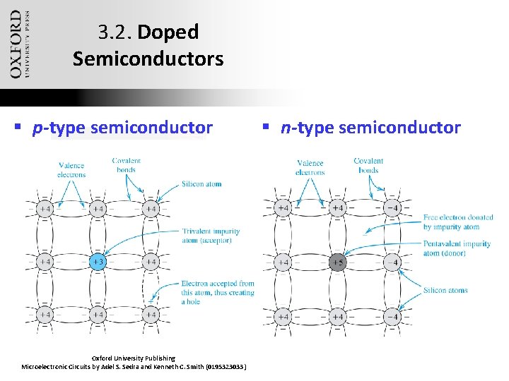
3. 2. Doped Semiconductors § p-type semiconductor § Silicon is doped with element having a valence of 3. § To increase the concentration of holes (p). § One example is boron. Oxford University Publishing Microelectronic Circuits by Adel S. Sedra and Kenneth C. Smith (0195323033) § n-type semiconductor § Silicon is doped with element having a valence of 5. § To increase the concentration of free electrons (n). § One example is phosophorus, which is a donor.
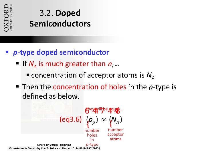
3. 2. Doped Semiconductors § p-type doped semiconductor § If NA is much greater than ni … § concentration of acceptor atoms is NA § Then the concentration of holes in the p-type is defined as below. Oxford University Publishing Microelectronic Circuits by Adel S. Sedra and Kenneth C. Smith (0195323033)
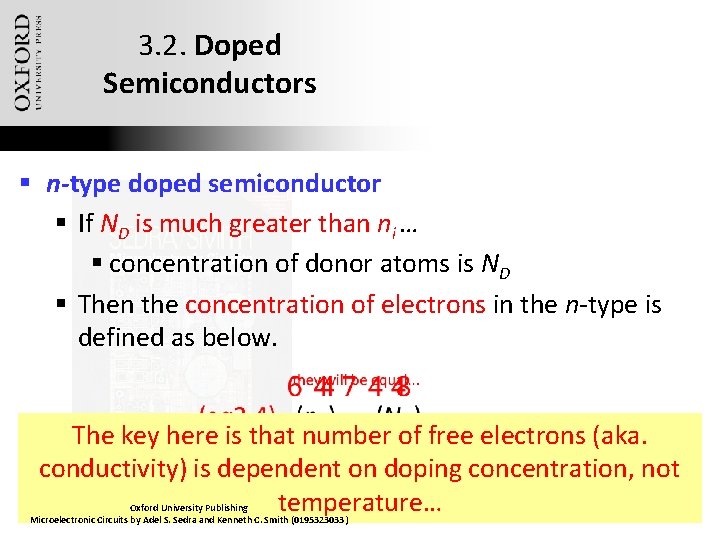
3. 2. Doped Semiconductors § n-type doped semiconductor § If ND is much greater than ni … § concentration of donor atoms is ND § Then the concentration of electrons in the n-type is defined as below. The key here is that number of free electrons (aka. conductivity) is dependent on doping concentration, not temperature… Oxford University Publishing Microelectronic Circuits by Adel S. Sedra and Kenneth C. Smith (0195323033)
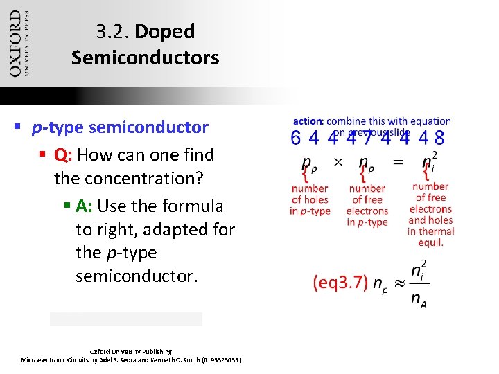
3. 2. Doped Semiconductors § p-type semiconductor § Q: How can one find the concentration? § A: Use the formula to right, adapted for the p-type semiconductor. Oxford University Publishing Microelectronic Circuits by Adel S. Sedra and Kenneth C. Smith (0195323033)
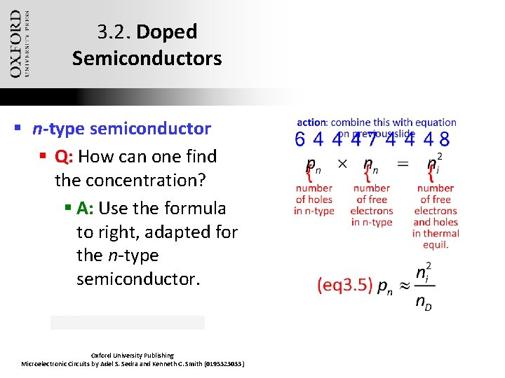
3. 2. Doped Semiconductors § n-type semiconductor § Q: How can one find the concentration? § A: Use the formula to right, adapted for the n-type semiconductor. Oxford University Publishing Microelectronic Circuits by Adel S. Sedra and Kenneth C. Smith (0195323033)
3. 2. Doped Semiconductors § p-type semiconductor § np will have the same dependence on temperature as ni 2 § the concentration of holes (pn) will be much larger than holes § holes are the majority charge carriers § free electrons are the minority charge carrier Oxford University Publishing Microelectronic Circuits by Adel S. Sedra and Kenneth C. Smith (0195323033) § n-type semiconductor § pn will have the same dependence on temperature as ni 2 § the concentration of free electrons (nn) will be much larger than holes § electrons are the majority charge carriers § holes are the minority charge carrier
Example 3. 2: Doped Semiconductor § Consider an n-type silicon for which the dopant concentration is ND = 1017/cm 3. Find the electron and hole concentrations at T = 300 K. Oxford University Publishing Microelectronic Circuits by Adel S. Sedra and Kenneth C. Smith (0195323033)
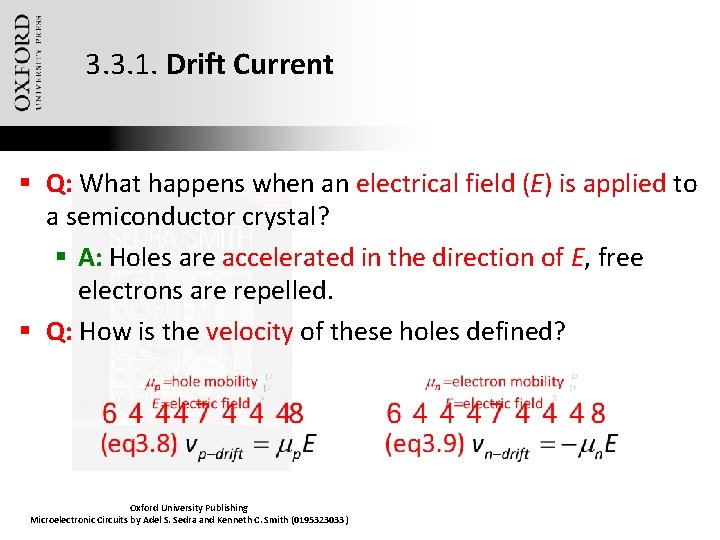
3. 3. 1. Drift Current § Q: What happens when an electrical field (E) is applied to a semiconductor crystal? § A: Holes are accelerated in the direction of E, free electrons are repelled. § Q: How is the velocity of these holes defined? Oxford University Publishing Microelectronic Circuits by Adel S. Sedra and Kenneth C. Smith (0195323033)
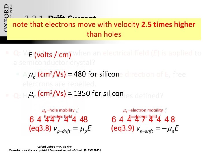
3. 3. 1. Drift Current note that electrons move with velocity 2. 5 times higher than holes § Q: What happens. E (volts / cm) when an electrical field (E) is applied to a semiconductor crystal? 2 are (cm /Vs)accelerated = 480 for silicon § A: . m. Holes in the direction of E, free p electrons are repelled. 2/Vs) = 1350 for silicon. m (cm n is the velocity of these holes defined? § Q: How Oxford University Publishing Microelectronic Circuits by Adel S. Sedra and Kenneth C. Smith (0195323033)
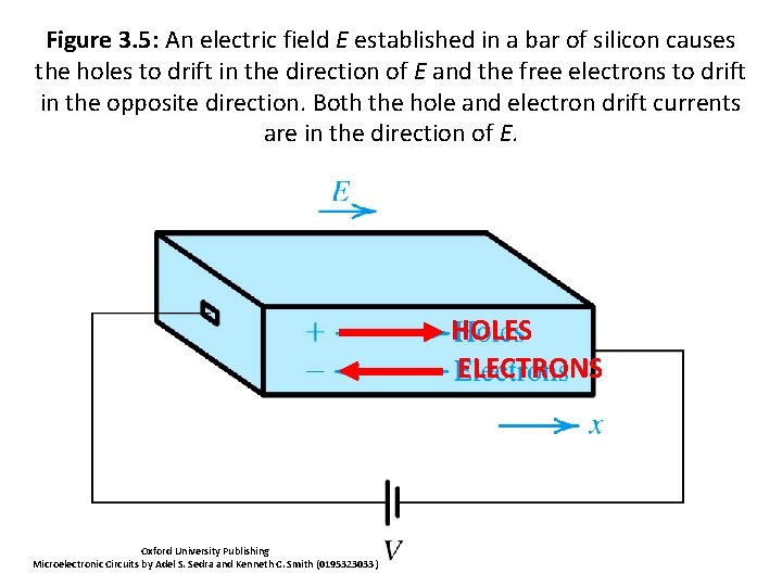
Figure 3. 5: An electric field E established in a bar of silicon causes the holes to drift in the direction of E and the free electrons to drift 3. 3. 1. Drift Current in the opposite direction. Both the hole and electron drift currents are in the direction of E. § Q: What happens when an electrical field (E) is applied to a semiconductor crystal? § A: Holes are accelerated in the direction of E, free electrons are repelled. HOLES § Q: How is the velocity of these holes defined? ELECTRONS Oxford University Publishing Microelectronic Circuits by Adel S. Sedra and Kenneth C. Smith (0195323033)
3. 3. 1. Drift Current § Assume that, for the single-crystal silicon bar on previous slide, the concentration of holes is defined as p and electrons as n. § Q: What is the current component attributed to the flow of holes (not electrons)? Oxford University Publishing Microelectronic Circuits by Adel S. Sedra and Kenneth C. Smith (0195323033)
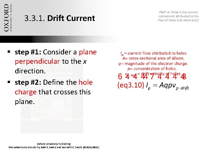
3. 3. 1. Drift Current § step #1: Consider a plane perpendicular to the x direction. § step #2: Define the hole charge that crosses this plane. Oxford University Publishing Microelectronic Circuits by Adel S. Sedra and Kenneth C. Smith (0195323033) PART A: What is the current component attributed to the flow of holes (not electrons)?
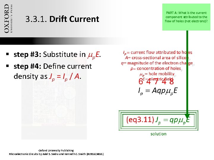
3. 3. 1. Drift Current § step #3: Substitute in mp. E. § step #4: Define current density as Jp = Ip / A. Oxford University Publishing Microelectronic Circuits by Adel S. Sedra and Kenneth C. Smith (0195323033) PART A: What is the current component attributed to the flow of holes (not electrons)?
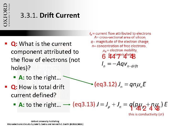
3. 3. 1. Drift Current § Q: What is the current component attributed to the flow of electrons (not holes)? § A: to the right… § Q: How is total drift current defined? § A: to the right… Oxford University Publishing Microelectronic Circuits by Adel S. Sedra and Kenneth C. Smith (0195323033)
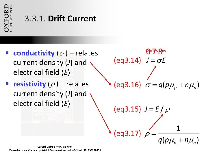
3. 3. 1. Drift Current § conductivity (s. ) – relates current density (J) and electrical field (E) § resistivity (r. ) – relates current density (J) and electrical field (E) Oxford University Publishing Microelectronic Circuits by Adel S. Sedra and Kenneth C. Smith (0195323033)
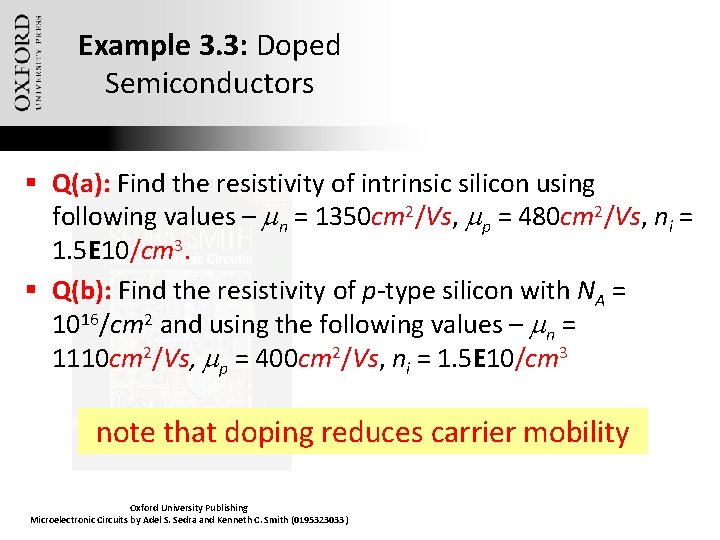
Example 3. 3: Doped Semiconductors § Q(a): Find the resistivity of intrinsic silicon using following values – mn = 1350 cm 2/Vs, mp = 480 cm 2/Vs, ni = 1. 5 E 10/cm 3. § Q(b): Find the resistivity of p-type silicon with NA = 1016/cm 2 and using the following values – mn = 1110 cm 2/Vs, mp = 400 cm 2/Vs, ni = 1. 5 E 10/cm 3 note that doping reduces carrier mobility Oxford University Publishing Microelectronic Circuits by Adel S. Sedra and Kenneth C. Smith (0195323033)
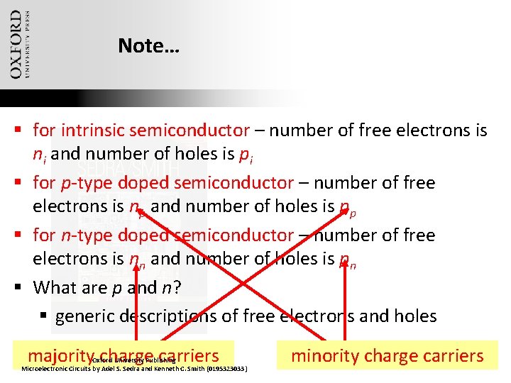
Note… § for intrinsic semiconductor – number of free electrons is ni and number of holes is pi § for p-type doped semiconductor – number of free electrons is np and number of holes is pp § for n-type doped semiconductor – number of free electrons is nn and number of holes is pn § What are p and n? § generic descriptions of free electrons and holes majority charge carriers Oxford University Publishing Microelectronic Circuits by Adel S. Sedra and Kenneth C. Smith (0195323033) minority charge carriers
3. 3. 2. Diffusion Current § carrier diffusion – is the flow of charge carriers from area of high concentration to low concentration. § It requires non-uniform distribution of carriers. § diffusion current – is the current flow that results from diffusion. Oxford University Publishing Microelectronic Circuits by Adel S. Sedra and Kenneth C. Smith (0195323033)
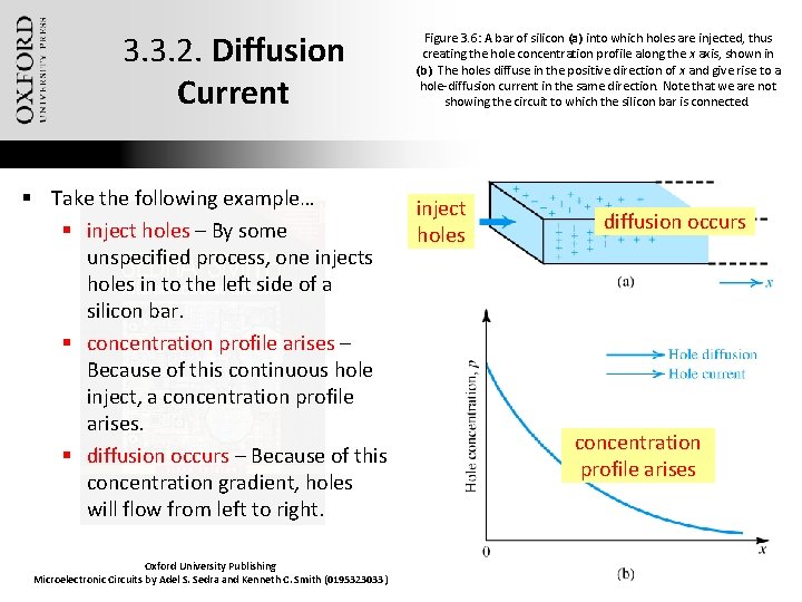
3. 3. 2. Diffusion Current § Take the following example… § inject holes – By some unspecified process, one injects holes in to the left side of a silicon bar. § concentration profile arises – Because of this continuous hole inject, a concentration profile arises. § diffusion occurs – Because of this concentration gradient, holes will flow from left to right. Oxford University Publishing Microelectronic Circuits by Adel S. Sedra and Kenneth C. Smith (0195323033) Figure 3. 6: A bar of silicon (a) into which holes are injected, thus creating the hole concentration profile along the x axis, shown in (b). The holes diffuse in the positive direction of x and give rise to a hole-diffusion current in the same direction. Note that we are not showing the circuit to which the silicon bar is connected. inject holes diffusion occurs concentration profile arises
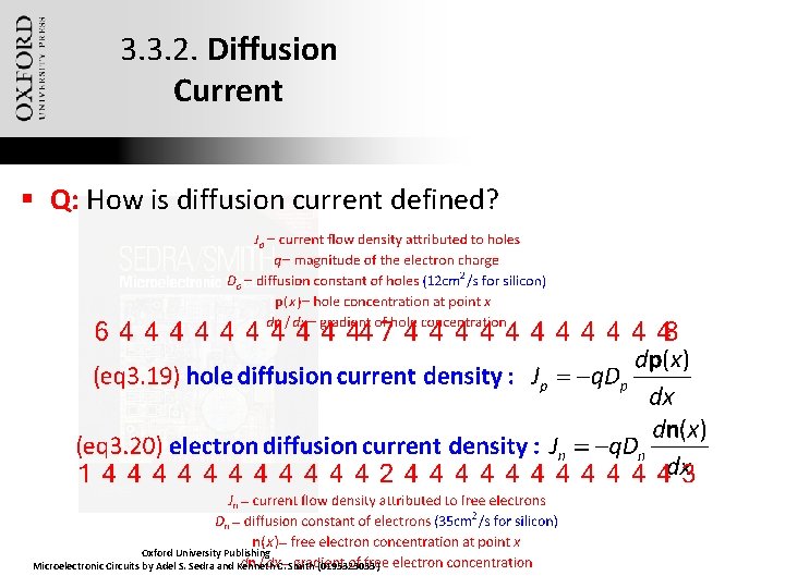
3. 3. 2. Diffusion Current § Q: How is diffusion current defined? Oxford University Publishing Microelectronic Circuits by Adel S. Sedra and Kenneth C. Smith (0195323033)
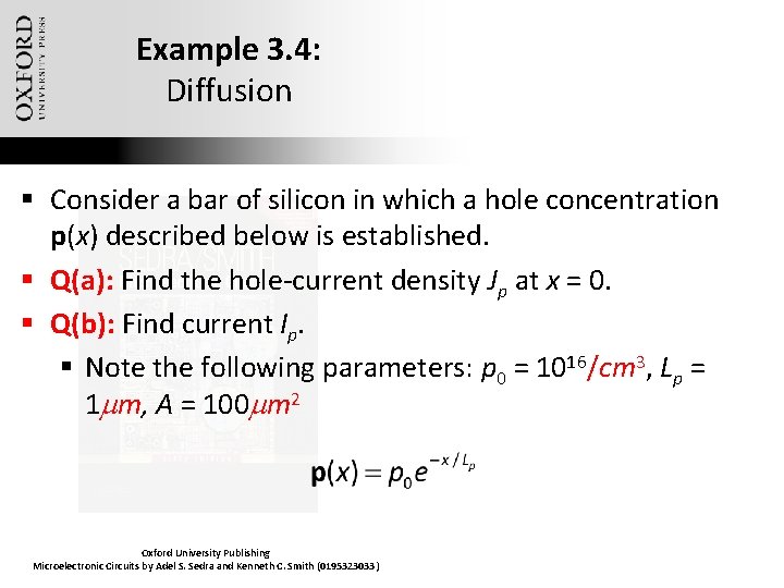
Example 3. 4: Diffusion § Consider a bar of silicon in which a hole concentration p(x) described below is established. § Q(a): Find the hole-current density Jp at x = 0. § Q(b): Find current Ip. § Note the following parameters: p 0 = 1016/cm 3, Lp = 1 mm, A = 100 mm 2 Oxford University Publishing Microelectronic Circuits by Adel S. Sedra and Kenneth C. Smith (0195323033)
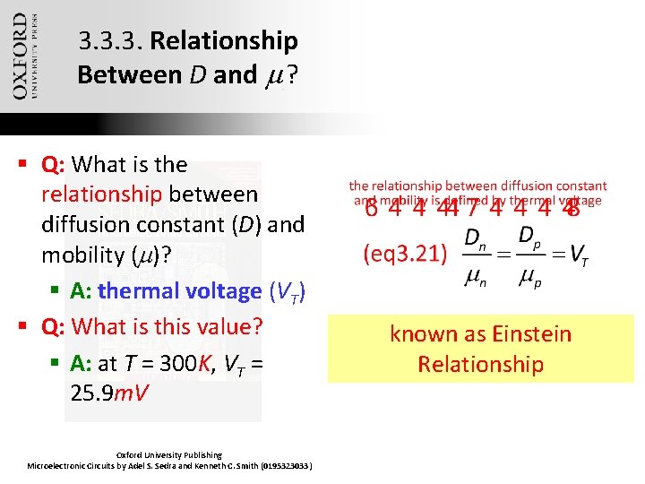
3. 3. 3. Relationship Between D and m. ? § Q: What is the relationship between diffusion constant (D) and mobility (m)? § A: thermal voltage (VT) § Q: What is this value? § A: at T = 300 K, VT = 25. 9 m. V Oxford University Publishing Microelectronic Circuits by Adel S. Sedra and Kenneth C. Smith (0195323033) known as Einstein Relationship
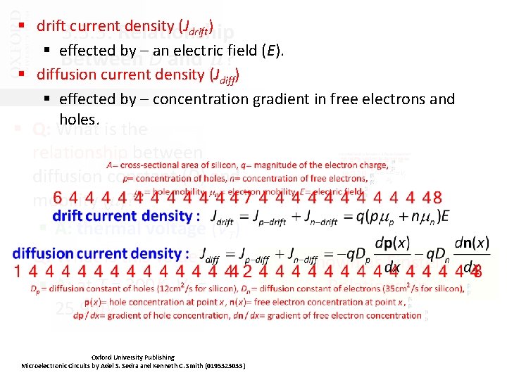
§ drift 3. 3. 3. current. Relationship density (Jdrift) § effected by – an electric field (E). Between D and m. ? § diffusion current density (Jdiff) § effected by – concentration gradient in free electrons and holes. § Q: What is the relationship between diffusion constant (D) and mobility (m)? § A: thermal voltage (VT) § Q: What is this value? § A: at T = 300 K, VT = 25. 9 m. V Oxford University Publishing Microelectronic Circuits by Adel S. Sedra and Kenneth C. Smith (0195323033) known as Einstein Relationship
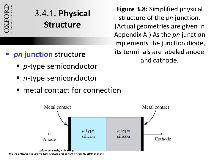
3. 4. 1. Physical Structure Figure 3. 8: Simplified physical structure of the pn junction. (Actual geometries are given in Appendix A. ) As the pn junction implements the junction diode, its terminals are labeled anode and cathode. § pn junction structure § p-type semiconductor § n-type semiconductor § metal contact for connection Oxford University Publishing Microelectronic Circuits by Adel S. Sedra and Kenneth C. Smith (0195323033)
3. 4. 2. Operation with Open-Circuit Terminals § Q: What is state of pn junction with open-circuit terminals? § A: Read the below… § p-type material contains majority of holes § these holes are neutralized by equal amount of bound negative charge § n-type material contains majority of free electrons § these electrons are neutralized by equal amount of bound positive charge Oxford University Publishing Microelectronic Circuits by Adel S. Sedra and Kenneth C. Smith (0195323033)

3. 4. 2. Operation with Open-Circuit Terminals § bound charge § charge of opposite polarity to free electrons / holes of a given material § neutralizes the electrical charge of these majority carriers § does not affect concentration gradients Oxford University Publishing Microelectronic Circuits by Adel S. Sedra and Kenneth C. Smith (0195323033)
3. 4. 2. Operation with Open-Circuit Terminals § Q: What happens when a pn-junction is newly formed – aka. when the p-type and n-type semiconductors first touch one another? § A: See following slides… Oxford University Publishing Microelectronic Circuits by Adel S. Sedra and Kenneth C. Smith (0195323033)
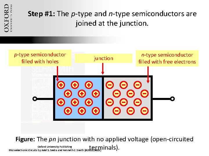
Step #1: The p-type and n-type semiconductors are joined at the junction. p-type semiconductor filled with holes junction n-type semiconductor filled with free electrons Figure: The pn junction with no applied voltage (open-circuited Oxford University Publishing terminals). Microelectronic Circuits by Adel S. Sedra and Kenneth C. Smith (0195323033)
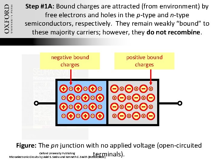
Step #1 A: Bound charges are attracted (from environment) by free electrons and holes in the p-type and n-type semiconductors, respectively. They remain weakly “bound” to these majority carriers; however, they do not recombine. negative bound charges positive bound charges Figure: The pn junction with no applied voltage (open-circuited Oxford University Publishing terminals). Microelectronic Circuits by Adel S. Sedra and Kenneth C. Smith (0195323033)
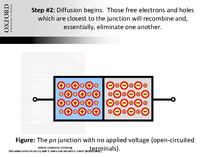
Step #2: Diffusion begins. Those free electrons and holes which are closest to the junction will recombine and, essentially, eliminate one another. Figure: The pn junction with no applied voltage (open-circuited Oxford University Publishing terminals). Microelectronic Circuits by Adel S. Sedra and Kenneth C. Smith (0195323033)
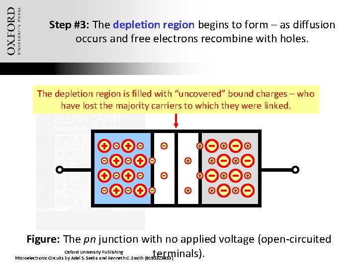
Step #3: The depletion region begins to form – as diffusion occurs and free electrons recombine with holes. The depletion region is filled with “uncovered” bound charges – who have lost the majority carriers to which they were linked. Figure: The pn junction with no applied voltage (open-circuited Oxford University Publishing terminals). Microelectronic Circuits by Adel S. Sedra and Kenneth C. Smith (0195323033)
3. 4. 2. Operation with Open-Circuit Terminals § Q: Why does diffusion occur even when bound charges neutralize the electrical attraction of majority carriers to one another? § A: Diffusion current, as shown in (3. 19) and (3. 20), is effected by a gradient in concentration of majority carriers – not an electrical attraction of these particles to one another. Oxford University Publishing Microelectronic Circuits by Adel S. Sedra and Kenneth C. Smith (0195323033)
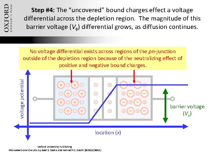
Step #4: The “uncovered” bound charges effect a voltage differential across the depletion region. The magnitude of this barrier voltage (V 0) differential grows, as diffusion continues. voltage potential No voltage differential exists across regions of the pn-junction outside of the depletion region because of the neutralizing effect of positive and negative bound charges. barrier voltage (Vo) location (x) Oxford University Publishing Microelectronic Circuits by Adel S. Sedra and Kenneth C. Smith (0195323033)
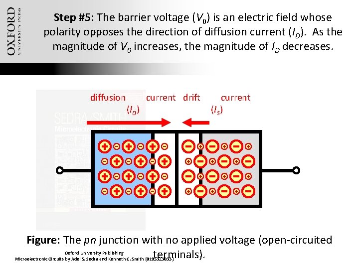
Step #5: The barrier voltage (V 0) is an electric field whose polarity opposes the direction of diffusion current (ID). As the magnitude of V 0 increases, the magnitude of ID decreases. diffusion (ID) current drift current (IS) Figure: The pn junction with no applied voltage (open-circuited Oxford University Publishing terminals). Microelectronic Circuits by Adel S. Sedra and Kenneth C. Smith (0195323033)
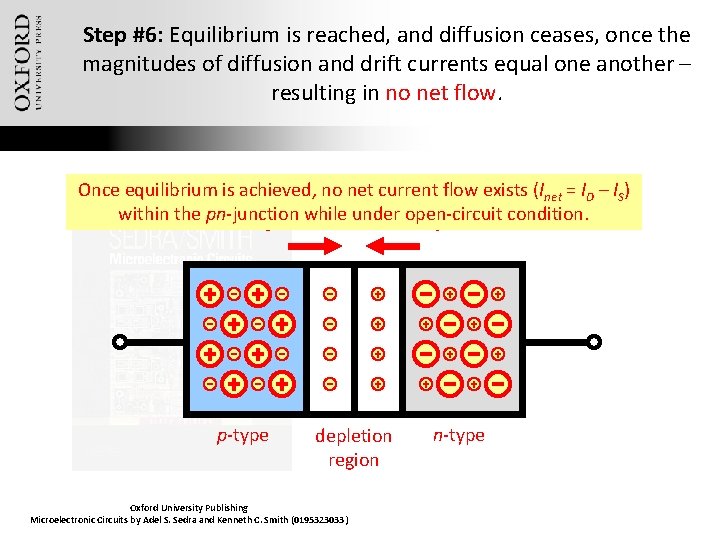
Step #6: Equilibrium is reached, and diffusion ceases, once the magnitudes of diffusion and drift currents equal one another – resulting in no net flow. Once equilibrium is achieved, no netdrift current flow exists (Inet = ID – IS) diffusion current within the pn-junction condition. (I ) while under open-circuit (I ) D p-type S depletion region Oxford University Publishing Microelectronic Circuits by Adel S. Sedra and Kenneth C. Smith (0195323033) n-type
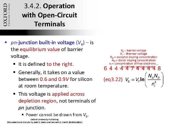
3. 4. 2. Operation with Open-Circuit Terminals § pn-junction built-in voltage (V 0) – is the equilibrium value of barrier voltage. § It is defined to the right. § Generally, it takes on a value between 0. 6 and 0. 9 V for silicon at room temperature. § This voltage is applied across depletion region, not terminals of pn junction. § Power cannot be drawn from V 0. Oxford University Publishing Microelectronic Circuits by Adel S. Sedra and Kenneth C. Smith (0195323033)
The Drift Current IS and Equilibrium § In addition to majority-carrier diffusion current (ID), a component of current due to minority carrier drift exists (IS). § Specifically, some of thermally generated holes in the p -type and n-type materials move toward and reach the edge of the depletion region. § There, they experience the electric field (V 0) in the depletion region and are swept across it. § Unlike diffusion current, the polarity of V 0 reinforces this drift current. Oxford University Publishing Microelectronic Circuits by Adel S. Sedra and Kenneth C. Smith (0195323033)
3. 4. 2. Operation with Open-Circuit Terminals § Because these holes are free electrons are produced by thermal energy, IS is heavily dependent on temperature § Any depletion-layer voltage, regardless of how small, will cause the transition across junction. Therefore IS is independent of V 0. § drift current (IS) – is the movement of these minority carriers. § aka. electrons from n-side to p-side of the junction Oxford University Publishing Microelectronic Circuits by Adel S. Sedra and Kenneth C. Smith (0195323033)
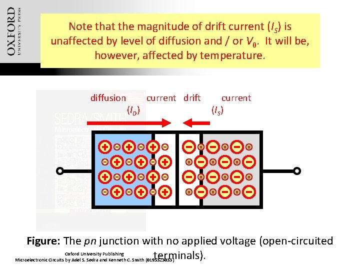
Note that the magnitude of drift current (IS) is unaffected by level of diffusion and / or V 0. It will be, however, affected by temperature. diffusion (ID) current drift current (IS) Figure: The pn junction with no applied voltage (open-circuited Oxford University Publishing terminals). Microelectronic Circuits by Adel S. Sedra and Kenneth C. Smith (0195323033)
3. 4. 2. Operation with Open-Circuit Terminals § Q: Is the depletion region always symmetrical? As shown on previous slides? § A: The short answer is no. § Q: Why? § Typically NA > ND § And, because concentration of doping agents (NA, ND) is unequal, the width of depletion region will differ from side to side. Oxford University Publishing Microelectronic Circuits by Adel S. Sedra and Kenneth C. Smith (0195323033)
3. 4. 2. Operation with Open-Circuit Terminals § Q: Why? § A: Because, typically NA > ND. § When the concentration of doping agents (NA, ND) is unequal, the width of depletion region will differ from side to side. § The depletion region will extend deeper in to the “less doped” material, a requirement to uncover the same amount of charge. § xp = width of depletion p-region Publishingof depletion n-region §Oxford xn. University = width Microelectronic Circuits by Adel S. Sedra and Kenneth C. Smith (0195323033)
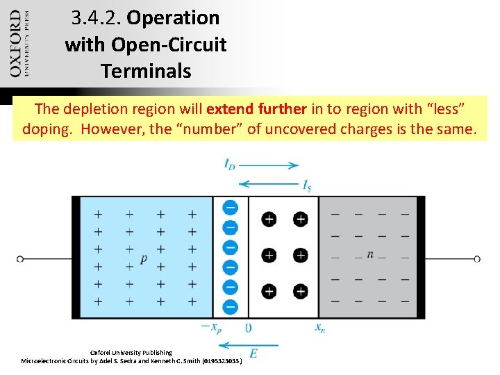
3. 4. 2. Operation with Open-Circuit Terminals The depletion region will extend further in to region with “less” doping. However, the “number” of uncovered charges is the same. Oxford University Publishing Microelectronic Circuits by Adel S. Sedra and Kenneth C. Smith (0195323033)
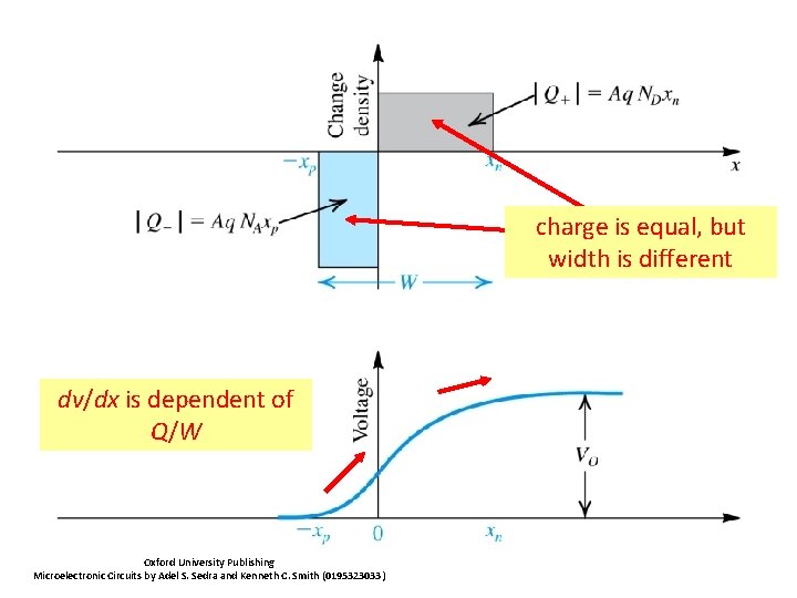
3. 4. 2: Operation with Open-Circuit Terminals § Width of and Charge Stored in the Depletion Region § the question we ask here is, what happens once the open-circuit pn junction reaches equilibrium? ? ? dv/dx is dependent § typically NA > ND of Q/W § minority carrier concentrations at equilibrium (no voltage applied) are denoted by np 0 University Publishing and p. Oxford Microelectronic Circuits by Adel S. Sedra and Kenneth C. Smith (0195323033) n 0 § because concentration of charge equal, but doping agentsis (N A, ND) is width different unequal, the is width of depletion region will differ from side to side § the depletion region will extend deeper in to the “less doped” material, a requirement to uncover the same amount of charge § xp = width of depletion
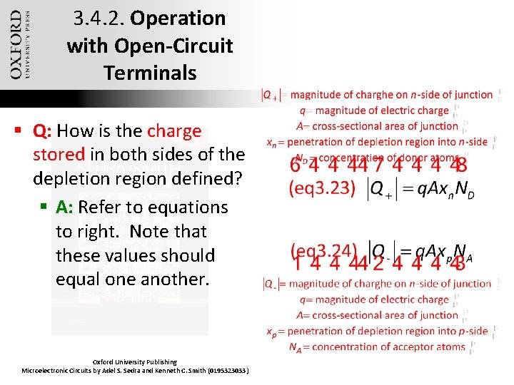
3. 4. 2. Operation with Open-Circuit Terminals § Q: How is the charge stored in both sides of the depletion region defined? § A: Refer to equations to right. Note that these values should equal one another. Oxford University Publishing Microelectronic Circuits by Adel S. Sedra and Kenneth C. Smith (0195323033)
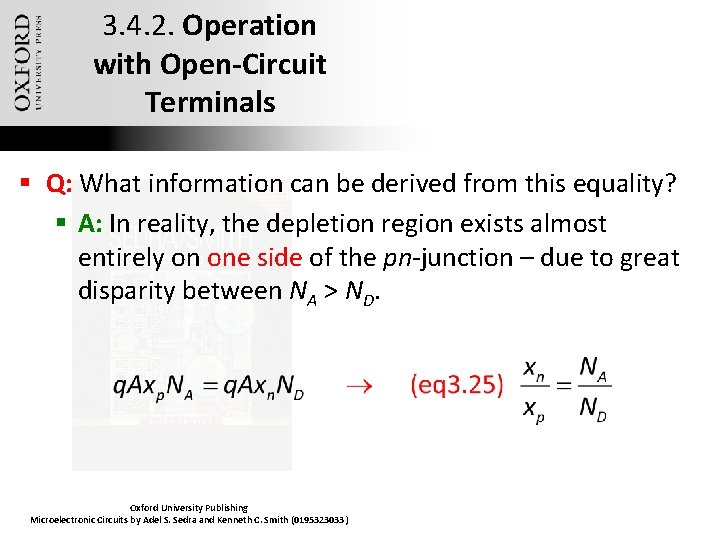
3. 4. 2. Operation with Open-Circuit Terminals § Q: What information can be derived from this equality? § A: In reality, the depletion region exists almost entirely on one side of the pn-junction – due to great disparity between NA > ND. Oxford University Publishing Microelectronic Circuits by Adel S. Sedra and Kenneth C. Smith (0195323033)
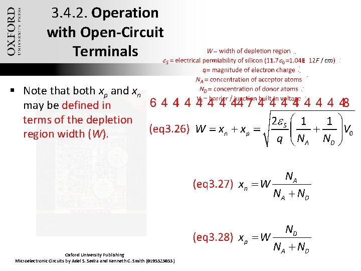
3. 4. 2. Operation with Open-Circuit Terminals § Note that both xp and xn may be defined in terms of the depletion region width (W). Oxford University Publishing Microelectronic Circuits by Adel S. Sedra and Kenneth C. Smith (0195323033)
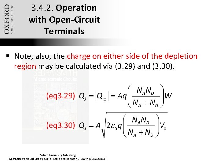
3. 4. 2. Operation with Open-Circuit Terminals § Note, also, the charge on either side of the depletion region may be calculated via (3. 29) and (3. 30). Oxford University Publishing Microelectronic Circuits by Adel S. Sedra and Kenneth C. Smith (0195323033)
Example 3. 5 § Refer to book… Oxford University Publishing Microelectronic Circuits by Adel S. Sedra and Kenneth C. Smith (0195323033)
3. 4. 2. Operation with Open-Circuit Terminals § Q: What has been learned about the pn-junction? § A: composition § The pn junction is composed of two silicon-based semiconductors, one doped to be p-type and the other n-type. § A: majority carriers § Are generated by doping. § Holes are present on p-side, free electrons are present on n-side. Oxford University Publishing Microelectronic Circuits by Adel S. Sedra and Kenneth C. Smith (0195323033)

3. 4. 2. Operation with Open-Circuit Terminals § Q: What has been learned about the pn-junction? § A: bound charges § Charge of majority carriers are neutralized electrically by bound charges. § A: diffusion current ID § Those majority carriers close to the junction will diffuse across, resulting in their elimination. Oxford University Publishing Microelectronic Circuits by Adel S. Sedra and Kenneth C. Smith (0195323033)

3. 4. 2. Operation with Open-Circuit Terminals § Q: What has been learned about the pn-junction? § A: depletion region § As these carriers disappear, they release bound charges and effect a voltage differential V 0. § A: depletion-layer voltage § As diffusion continues, the depletion layer voltage (V 0) grows, making diffusion more difficult and eventually bringing it to halt. Oxford University Publishing Microelectronic Circuits by Adel S. Sedra and Kenneth C. Smith (0195323033)
3. 4. 2. Operation with Open-Circuit Terminals § Q: What has been learned about the pn-junction? § A: minority carriers § Are generated thermally. § Free electrons are present on p-side, holes are present on n-side. § A: drift current IS § The depletion-layer voltage (V 0) facilitates the flow of minority carriers to opposite side. § A: open circuit equilibrium ID = IS Oxford University Publishing Microelectronic Circuits by Adel S. Sedra and Kenneth C. Smith (0195323033)
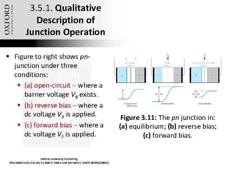
3. 5. 1. Qualitative Description of Junction Operation § Figure to right shows pnjunction under three conditions: § (a) open-circuit – where a barrier voltage V 0 exists. § (b) reverse bias – where a dc voltage VR is applied. § (c) forward bias – where a dc voltage VF is applied. Oxford University Publishing Microelectronic Circuits by Adel S. Sedra and Kenneth C. Smith (0195323033) Figure 3. 11: The pn junction in: (a) equilibrium; (b) reverse bias; (c) forward bias.
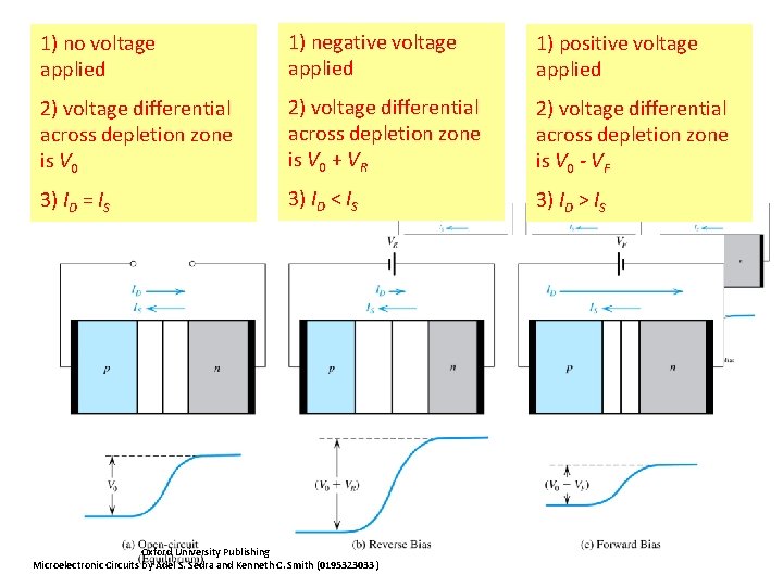
1) no voltage applied 1) negative voltage applied 1) positive voltage applied 2) voltage differential across depletion zone is V 0 + VR 2) voltage differential across depletion zone is V 0 - VF § 3)Figure 3) ID < IS ID = IS to right shows pnjunction under three conditions: § (a) open-circuit – where a barrier voltage V 0 exists. § (b) reverse bias – where a dc voltage VR is applied. § (c) forward bias – where a dc voltage VF is applied. Oxford University Publishing Microelectronic Circuits by Adel S. Sedra and Kenneth C. Smith (0195323033) 3) ID > IS Figure 3. 11: The pn junction in: (a) equilibrium; (b) reverse bias; (c) forward bias.
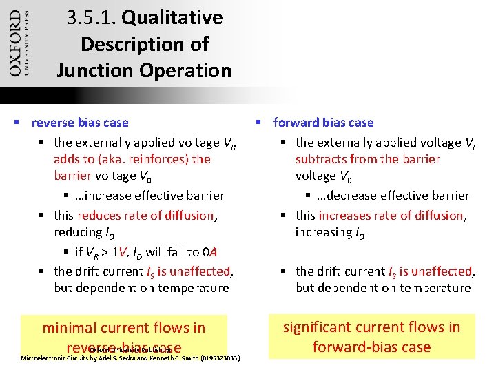
3. 5. 1. Qualitative Description of Junction Operation § reverse bias case § the externally applied voltage VR adds to (aka. reinforces) the barrier voltage V 0 § …increase effective barrier § this reduces rate of diffusion, reducing ID § if VR > 1 V, ID will fall to 0 A § the drift current IS is unaffected, but dependent on temperature § result is that pn junction will conduct current small driftflows current minimal in IS reverse-bias case Oxford University Publishing Microelectronic Circuits by Adel S. Sedra and Kenneth C. Smith (0195323033) § forward bias case § the externally applied voltage VF subtracts from the barrier voltage V 0 § …decrease effective barrier § this increases rate of diffusion, increasing ID § k § the drift current IS is unaffected, but dependent on temperature § result is that pn junction will conduct significant ID - IS significant current flows in forward-bias case

Forward-Bias Case § Observe that decreased barrier voltage will be accompanied by… § (1) decrease in stored uncovered charge on both sides of junction § (2) smaller depletion region § Width of depletion region shown to right. Oxford University Publishing Microelectronic Circuits by Adel S. Sedra and Kenneth C. Smith (0195323033)
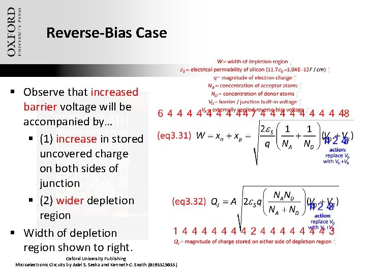
Reverse-Bias Case § Observe that increased barrier voltage will be accompanied by… § (1) increase in stored uncovered charge on both sides of junction § (2) wider depletion region § Width of depletion region shown to right. Oxford University Publishing Microelectronic Circuits by Adel S. Sedra and Kenneth C. Smith (0195323033)
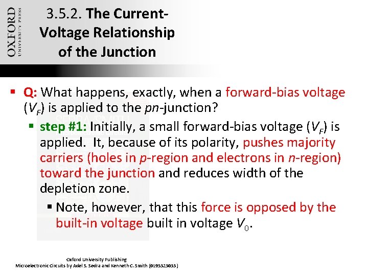
3. 5. 2. The Current. Voltage Relationship of the Junction § Q: What happens, exactly, when a forward-bias voltage (VF) is applied to the pn-junction? § step #1: Initially, a small forward-bias voltage (VF) is applied. It, because of its polarity, pushes majority carriers (holes in p-region and electrons in n-region) toward the junction and reduces width of the depletion zone. § Note, however, that this force is opposed by the built-in voltage built in voltage V 0. Oxford University Publishing Microelectronic Circuits by Adel S. Sedra and Kenneth C. Smith (0195323033)
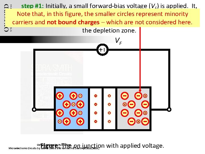
step #1: Initially, a small forward-bias voltage (VF) is applied. It, Note that, in figure, the smaller circles(holes represent minority because ofthis its polarity, pushes majority in p-region and carriers and not bound charges which are not considered here. of electrons in n-region) toward–the junction and reduces width the depletion zone. VF Figure: The pn junction with applied voltage. Oxford University Publishing Microelectronic Circuits by Adel S. Sedra and Kenneth C. Smith (0195323033)
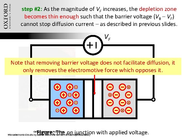
step #2: As the magnitude of VF increases, the depletion zone becomes thin enough such that the barrier voltage (V 0 – VF) cannot stop diffusion current – as described in previous slides. VF Note that removing barrier voltage does not facilitate diffusion, it only removes the electromotive force which opposes it. Figure: The pn junction with applied voltage. Oxford University Publishing Microelectronic Circuits by Adel S. Sedra and Kenneth C. Smith (0195323033)

step #3: Majority carriers (free electrons in n-region and holes in p-region) cross the junction and become minority charge carriers in the near-neutral region. VF diffusion current (ID) drift current (IS) Figure: The pn junction with applied voltage. Oxford University Publishing Microelectronic Circuits by Adel S. Sedra and Kenneth C. Smith (0195323033)
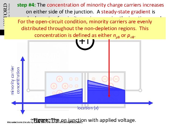
minority carrier concentration step #4: The concentration of minority charge carriers increases on either side of the junction. A steady-state gradient is reached as rate of majority carriers crossing the junction equals For the open-circuit condition, minority carriers are evenly that of recombination. distributed throughout the non-depletion regions. This F concentration is defined as. Veither np 0 or pn 0. location (x) Figure: The pn junction with applied voltage. Oxford University Publishing Microelectronic Circuits by Adel S. Sedra and Kenneth C. Smith (0195323033)
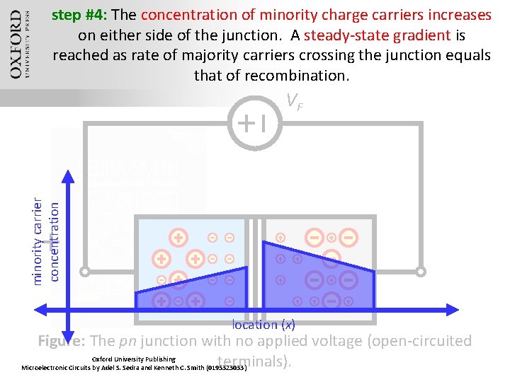
step #4: The concentration of minority charge carriers increases on either side of the junction. A steady-state gradient is reached as rate of majority carriers crossing the junction equals that of recombination. minority carrier concentration VF location (x) Figure: The pn junction with no applied voltage (open-circuited Oxford University Publishing terminals). Microelectronic Circuits by Adel S. Sedra and Kenneth C. Smith (0195323033)
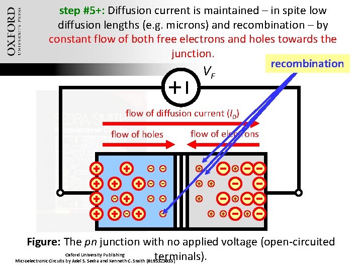
step #5+: Diffusion current is maintained – in spite low diffusion lengths (e. g. microns) and recombination – by constant flow of both free electrons and holes towards the junction. recombination VF flow of diffusion current (ID) flow of holes flow of electrons Figure: The pn junction with no applied voltage (open-circuited Oxford University Publishing terminals). Microelectronic Circuits by Adel S. Sedra and Kenneth C. Smith (0195323033)
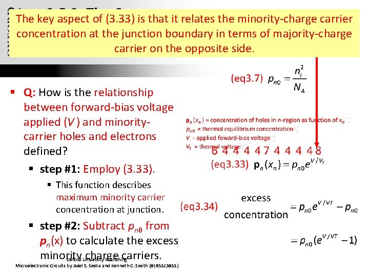
3. 5. 2. Current. The key aspect. The of (3. 33) is that it relates the minority-charge carrier concentration the junction boundary in terms of majority-charge Voltageat. Relationship carrier on the opposite side. of the Junction § Q: How is the relationship between forward-bias voltage applied (V. ) and minoritycarrier holes and electrons defined? § step #1: Employ (3. 33). § This function describes maximum minority carrier concentration at junction. § step #2: Subtract pn 0 from pn(x) to calculate the excess minority charge carriers. Oxford University Publishing Microelectronic Circuits by Adel S. Sedra and Kenneth C. Smith (0195323033)
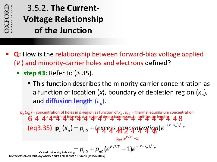
3. 5. 2. The Current. Voltage Relationship of the Junction § Q: How is the relationship between forward-bias voltage applied (V. ) and minority-carrier holes and electrons defined? § step #3: Refer to (3. 35). § This function describes the minority carrier concentration as a function of location (x), boundary of depletion region (xn), and diffusion length (Lp). Oxford University Publishing Microelectronic Circuits by Adel S. Sedra and Kenneth C. Smith (0195323033)
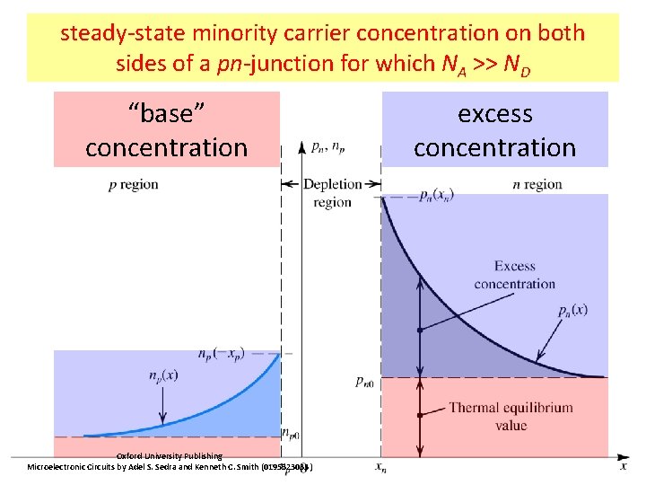
3. 5. 2: The Current-Voltage steady-state minority carrier concentration on both Relationship of the sides of a pn-junction for which NA >> ND Junction “base” concentration Oxford University Publishing Microelectronic Circuits by Adel S. Sedra and Kenneth C. Smith (0195323033) excess concentration
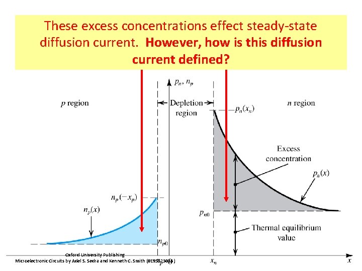
3. 5. 2: The Current-Voltage These excess concentrations effect steady-state Relationship of the diffusion. Junction current. However, how is this diffusion current defined? Oxford University Publishing Microelectronic Circuits by Adel S. Sedra and Kenneth C. Smith (0195323033)
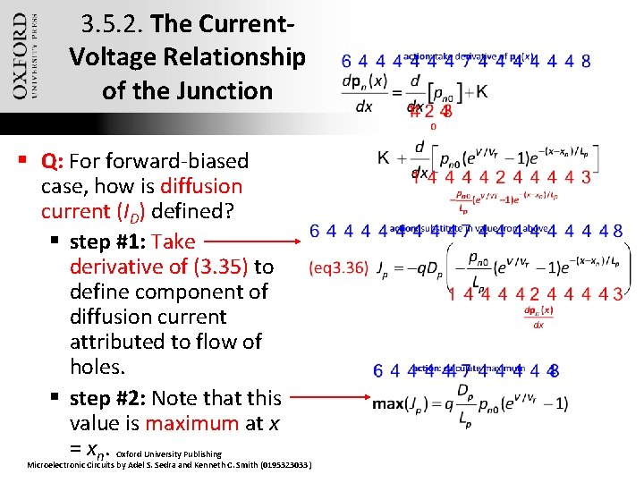
3. 5. 2. The Current. Voltage Relationship of the Junction § Q: For forward-biased case, how is diffusion current (ID) defined? § step #1: Take derivative of (3. 35) to define component of diffusion current attributed to flow of holes. § step #2: Note that this value is maximum at x = xn. Oxford University Publishing Microelectronic Circuits by Adel S. Sedra and Kenneth C. Smith (0195323033)
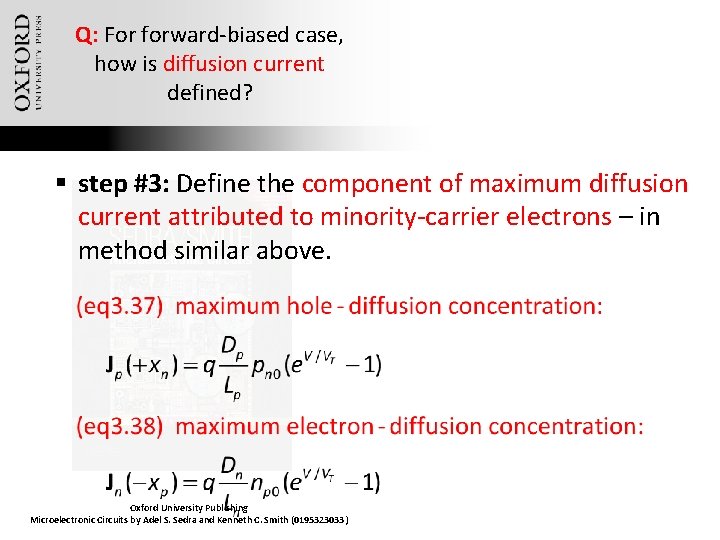
Q: For forward-biased case, how is diffusion current defined? § step #3: Define the component of maximum diffusion current attributed to minority-carrier electrons – in method similar above. Oxford University Publishing Microelectronic Circuits by Adel S. Sedra and Kenneth C. Smith (0195323033)
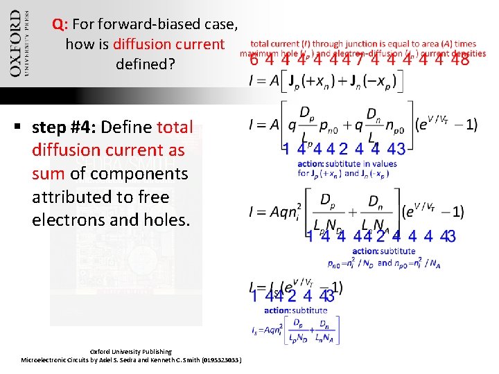
Q: For forward-biased case, how is diffusion current defined? § step #4: Define total diffusion current as sum of components attributed to free electrons and holes. Oxford University Publishing Microelectronic Circuits by Adel S. Sedra and Kenneth C. Smith (0195323033)
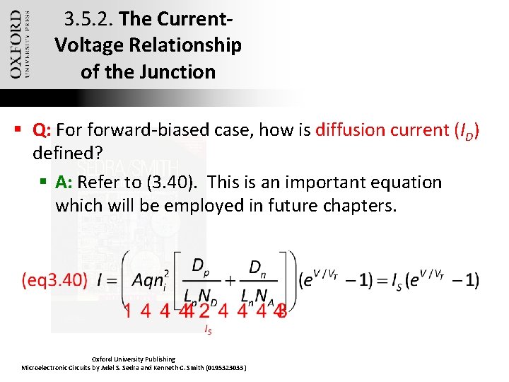
3. 5. 2. The Current. Voltage Relationship of the Junction § Q: For forward-biased case, how is diffusion current (ID) defined? § A: Refer to (3. 40). This is an important equation which will be employed in future chapters. Oxford University Publishing Microelectronic Circuits by Adel S. Sedra and Kenneth C. Smith (0195323033)
3. 5. 2. The Current. Voltage Relationship of the Junction § Q: Why is diffusion current (ID) dependent on the concentration gradient of minority (as opposed to majority) charge carriers? § A: Essentially, it isn’t. § Equation (3. 33) defines the minority-charge carrier concentration in terms of the majority-charge carrier concentrations in “other” region. § As such, the diffusion current (ID) is most dependent on two factors: applied forward-bias voltage (VF) and doping. Oxford University Publishing Microelectronic Circuits by Adel S. Sedra and Kenneth C. Smith (0195323033)
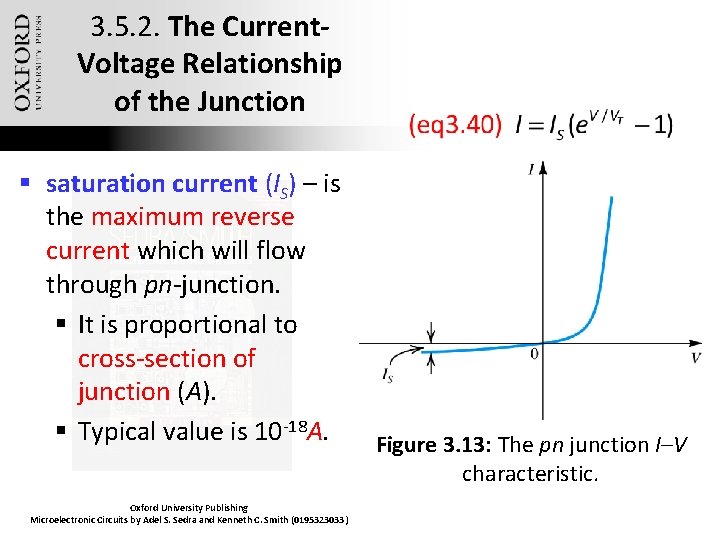
3. 5. 2. The Current. Voltage Relationship of the Junction § saturation current (IS) – is the maximum reverse current which will flow through pn-junction. § It is proportional to cross-section of junction (A). § Typical value is 10 -18 A. Oxford University Publishing Microelectronic Circuits by Adel S. Sedra and Kenneth C. Smith (0195323033) Figure 3. 13: The pn junction I–V characteristic.
Example 3. 6: pn. Junction § Consider a forward-biased pn junction conducting a current of I = 0. 1 m. A with following parameters: § NA = 1018/cm 3, ND = 1016/cm 3, A = 10 -4 cm 2, ni = 1. 5 E 10/cm 3, Lp = 5 um, Ln = 10 um, Dp (n-region) = 10 cm 2/s, Dn (p-region) = 18 cm 2/s § Q(a): Calculate IS. § Q(b): Calculate the forward bias voltage (V). § Q(c): Component of current I due to hole injection and electron injection across the junction Oxford University Publishing Microelectronic Circuits by Adel S. Sedra and Kenneth C. Smith (0195323033)
Summary (1) § Today’s microelectronics technology is almost entirely based on the semiconductor silicon. If a circuit is to be fabricated as a monolithic integrated circuit (IC), it is made using a single silicon crystal, no matter how large the circuit is. § In a crystal of intrinsic or pure silicon, the atoms are held in position by covalent bonds. At very low temperatures, all the bonds are intact; No charge carriers are available to conduct current. As such, at these low temperatures, silicone acts as an insulator. Oxford University Publishing Microelectronic Circuits by Adel S. Sedra and Kenneth C. Smith (0195323033)
Summary (2) § At room temperature, thermal energy causes some of the covalent bonds to break, thus generating free electrons and holes that become available to conduct electricity. § Current in semiconductors is carried by free electrons and holes. Their numbers are equal and relatively small in intrinsic silicon. § The conductivity of silicon may be increased drastically by introducing small amounts of appropriate impurity materials into the silicon crystal – via process called doping. Oxford University Publishing Microelectronic Circuits by Adel S. Sedra and Kenneth C. Smith (0195323033)
Summary (3) § There are two kinds of doped semiconductor: n-type in which electrons are abundant, p-type in which holes are abundant. § There are two mechanisms for the transport of charge carriers in a semiconductor: drift and diffusion. § Carrier drift results when an electric field (E) is applied across a piece of silicon. The electric field accelerates the holes in the direction of E and electrons oppositely. These two currents sum to produce drift current in the direction of E. Oxford University Publishing Microelectronic Circuits by Adel S. Sedra and Kenneth C. Smith (0195323033)
Summary (4) § Carrier diffusion occurs when the concentration of charge carriers is made higher in one part of a silicon crystal than others. To establish a steady-state diffusion current, a carrier concentration must be maintained in the silicon crystal. § A basic semiconductor structure is the pn-junction. It is fabricated in a silicon crystal by creating a p-region in proximity to an n-region. The pn-junction is a diode and plays a dominant role in the structure and operation of transistors. Oxford University Publishing Microelectronic Circuits by Adel S. Sedra and Kenneth C. Smith (0195323033)
Summary (5) § When the terminals of the pn-junction are left open, no current flows externally. However, two equal and opposite currents (ID and IS) flow across the junction. Equilibrium is maintained by a built-in voltage (V 0). Note, however, that the voltage across an open junction is 0 V, since V 0 is cancelled by potentials appearing at the metal-to-semiconductor connection interfaces. § The voltage V 0 appears across the depletion region, which extends on both sides of the junction. Oxford University Publishing Microelectronic Circuits by Adel S. Sedra and Kenneth C. Smith (0195323033)
Summary (6) § The drift current IS is carried by thermally generated minority electrons in the p-material that are swept across the depletion region into the n-side. The opposite occurs in the n-material. IS flows from n to p, in the reverse direction of the junction. Its value is a strong function of temperature, but independent of V 0. § Forward biasing of the pn-junction, that is applying an external voltage that makes p more positive than n, reduces the barrier voltage to V 0 - V and results in an exponential increase in ID (while IS remains unchanged). Oxford University Publishing Microelectronic Circuits by Adel S. Sedra and Kenneth C. Smith (0195323033)
Summary (7) § The drift current IS is carried by thermally generated minority electrons in the p-material that are swept across the depletion region into the n-side. The opposite occurs in the n-material. IS flows from n to p, in the reverse direction of the junction. Its value is a strong function of temperature, but independent of V 0. § Forward biasing of the pn-junction, that is applying an external voltage that makes p more positive than n, reduces the barrier voltage to V 0 - V and results in an exponential increase in ID (while IS remains unchanged). Oxford University Publishing Microelectronic Circuits by Adel S. Sedra and Kenneth C. Smith (0195323033)
- Slides: 97