Nhanced Semiconductor PreIrradiation Wafer Testing For HLLHC Upgrade


 technology enables a")


- Slides: 25
Nhanced Semiconductor Pre-Irradiation Wafer Testing For HL-LHC Upgrade Josh Everts
Underlying Principles Particles pass through the detector and collide with atoms in the silicon This collision ‘knocks out’ electrons from atoms These electrons traverse an electric field created by an applied potential (bias potential) inside the silicon wafer Finally, the electrons travel to outside circuitry, through amplifiers and shapers, to generate a signal for analysis
Si. O 2 N+ P+ P-Bulk P+ Aluminum Back Contact V < -170 V Aluminum Gate N+ P+ P-Bulk N+
Nhanced Semiconductor Manufacturing Process and Production Goals Silicon On Insulator (SOI) technology enables a thinner wafer without breakage or damage to machinery First time the company has produced embedded polysilicon resistors. Goal is to create uniform resistances Demonstrate uniformity across wafers and structures.
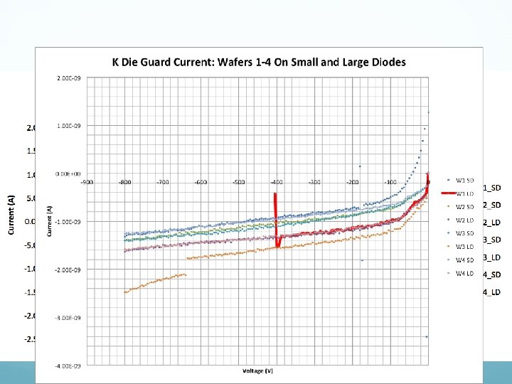
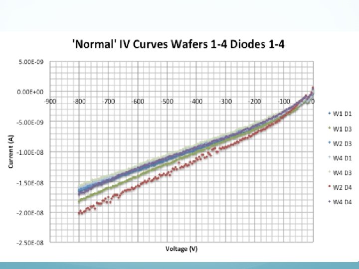
Guard Contact Diode Contact Small and Large Diode I-V Results
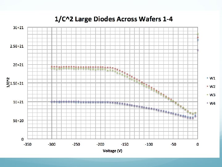
Probe Contact Small and Large Diode C-V Results
Small and Large Diode Conclusions Silicon resists breakdown across nearly all tested wafers indicating low levels of impurities Leakage currents are low indicating that the guard ring is providing good isolation C-V curve indicates full depletion at 170 V-close to the expected value.
“Effective Edge” J-Die Diode I-V Results Wafer Edge
J Die Diode Conclusions I-V Curves show that a majority of diodes go into breakdown early, indicating that structures this close the edge are prone to the effects of edge currents Building structures this close to the ‘effective edge’ is not viable
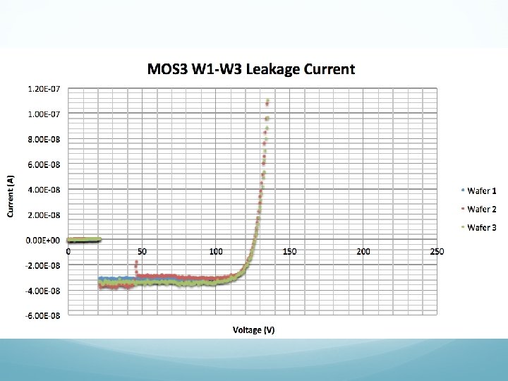
MOS C-V Results Probe Contact
MOS 1: Oxide Thickness: 4 microns Capacitance: 2. 16 nano. Farad (. 863 n. F/cm^2) MOS 2: Oxide Thickness: 5 microns Capacitance: 2. 5 nano. Farad (. 690 n. F/cm^2) MOS 3 Capacitance: 4. 75 nano. Farad (21. 6 n. F/cm 2) MOS 3 Oxide Thickness: 0. 17 microns Expected MOS 3: 5. 30 nano. Farad (24 n. F/cm 2) 0. 10 microns
Probe 1 “Far Complex” Probe 2 Polysilicon Resistor Results “Near Complex”
Ohms per square Values: Target: 1000 Ohms/square W 1: 720 -800 Ohms/square W 2: 750 -860 Ohms/square W 3: 800 -950 Ohms/square W 4: 840 -1000 Ohms/square
Polysilicon Resistor Conclusions Overall resistances are consistent between complexes on each wafer although less than expected Manufacturing differences have caused large variation between resistances on different wafers, this must be fixed before further use in AC coupled strip detectors Series resistances are somewhat inconsistent illustrating some difficulties with manufacturing
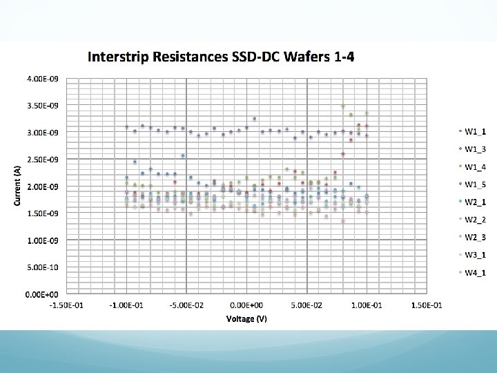
Keithley 617 Ammeter Keithley 617 Source from -0. 1 to 0. 1 V Keithley 617 Ammeter Interstrip Resistance Results
Interstrip Resistance Conclusions P-stops are working correctly as resistances are >1 giga. Ohm for wafers 2 -4 and around 0. 5 giga. Ohm for wafer 1 Further testing with a more accurate setup (lower humidity, measuring voltage drop with a current source) is required for truly accurate measurements
1 Probe to HP 2410 @ 200 V 2 Probe to HP 2410 @ 200 V Breakdown Voltage Results 3
Breakdown Voltage Conclusions Breakdowns are expected with this test but the oxide layer held up surprisingly well, especially in the strip detector. This, and the higher breakdown voltages suggest a high uniformity of oxide thickness and good resistivity
Summary Small and Large Diodes are well constructed and underlying bulk silicon is high quality J-Die Diodes suffer from early breakdown, especially near the edge of the wafer. In general, detector pixels/strips must be further from the edge to avoid these effects Polysilicon Resistors function well, however ohms/square values don’t match up with each other or expected values. P-stops and guard rings function well Oxide Capacitances are at expected values, along with leakage currents
Thank you for listening! Special thanks to: Ron Lipton, Rosemary Halenza, Zoltan Gecse, Petra Merkel, and the whole of the Si. Det Lab D team. Additional thanks to: Hannsjörg Weber and the HEP forum for organizing and hosting this talk as well as The University of Chicago for funding.