Lecture 28 PMOS LAST TIME NMOS Electrical Model
- Slides: 23

Lecture #28 PMOS • LAST TIME: NMOS Electrical Model – NMOS physical structure: W and L and dox, • TODAY: PMOS – Physical structure – CMOS – Dynamic circuits (Ring oscillators) 11/5/2004 EE 42 fall 2004 lecture 28 1

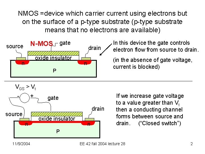
NMOS =device which carrier current using electrons but on the surface of a p-type substrate (p-type substrate means that no electrons are available) N-MOS gate source oxide insulator n drain In this device the gate controls electron flow from source to drain. (in the absence of gate voltage, current is blocked) n P VGS > Vt - + gate drain source n oxide insulator n If we increase gate voltage to a value greater than Vt then a conducting channel forms between source and drain. (“Closed switch”) P 11/5/2004 EE 42 fall 2004 lecture 28 2

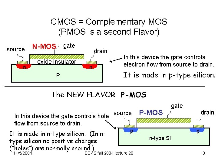
CMOS = Complementary MOS (PMOS is a second Flavor) source n N-MOS gate oxide insulator drain n P In this device the gate controls electron flow from source to drain. It is made in p-type silicon. The NEW FLAVOR! P-MOS In this device the gate controls hole flow from source to drain. It is made in n-type silicon. (In ntype silicon no positive charges (“holes”) are normally around. ) 11/5/2004 source P-MOS p EE 42 fall 2004 lecture 28 gate drain p n-type Si 3

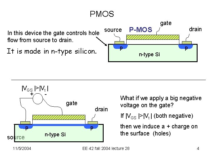
PMOS In this device the gate controls hole flow from source to drain. source It is made in n-type silicon. |VGS |>|Vt | + gate p p source 11/5/2004 drain n-type Si P-MOS p gate drain p n-type Si What if we apply a big negative voltage on the gate? If |VGS |>|Vt | (both negative) then we induce a + charge on the surface (holes) EE 42 fall 2004 lecture 28 4

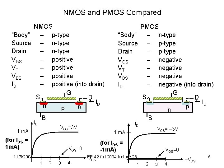
NMOS and PMOS Compared NMOS “Body” – p-type Source – n-type Drain – n-type VGS – positive VT – positive VDS – positive ID – positive (into drain) G S D ID n n p ID B ID VGS=3 V 1 m. A (for IDS = 1 m. A) 1 2 3 4 VGS= 3 V 1 m. A (for IDS = -1 m. A) VGS=0 11/5/2004 PMOS “Body” – n-type Source – p-type Drain – p-type VGS – negative VT – negative VDS – negative ID – negative (into drain) G S D ID p n B VGS=0 EE V 42 fall 2004 lecture 28 DS 1 2 3 4 VDS 5

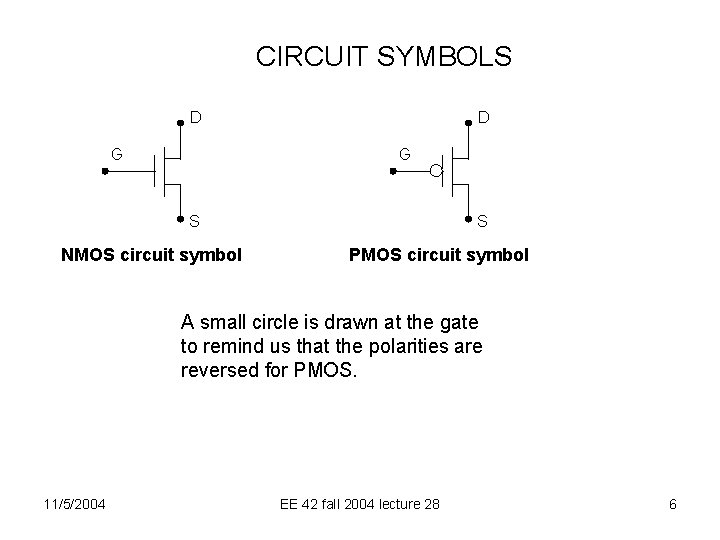
CIRCUIT SYMBOLS D G S NMOS circuit symbol S PMOS circuit symbol A small circle is drawn at the gate to remind us that the polarities are reversed for PMOS. 11/5/2004 EE 42 fall 2004 lecture 28 6

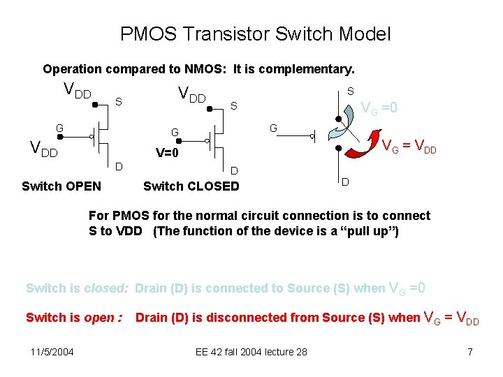
PMOS Transistor Switch Model Operation compared to NMOS: It is complementary. VDD S G G VDD VG =0 S VG = VDD V=0 D Switch OPEN D Switch CLOSED D For PMOS for the normal circuit connection is to connect S to VDD (The function of the device is a “pull up”) Switch is closed: Drain (D) is connected to Source (S) when VG =0 Switch is open : 11/5/2004 Drain (D) is disconnected from Source (S) when VG = VDD EE 42 fall 2004 lecture 28 7

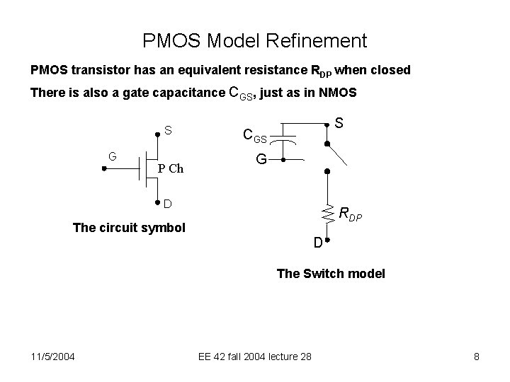
PMOS Model Refinement PMOS transistor has an equivalent resistance RDP when closed There is also a gate capacitance CGS, just as in NMOS S G P Ch S CGS G D RDP The circuit symbol D The Switch model 11/5/2004 EE 42 fall 2004 lecture 28 8

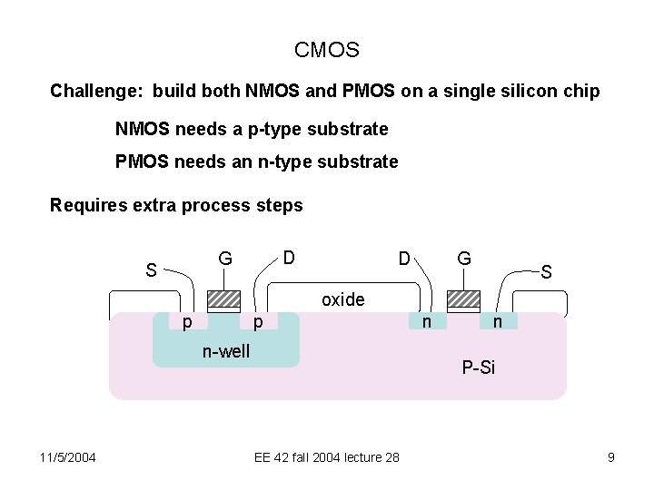
CMOS Challenge: build both NMOS and PMOS on a single silicon chip NMOS needs a p-type substrate PMOS needs an n-type substrate Requires extra process steps D G S G D S oxide p p n-well 11/5/2004 n n P-Si EE 42 fall 2004 lecture 28 9

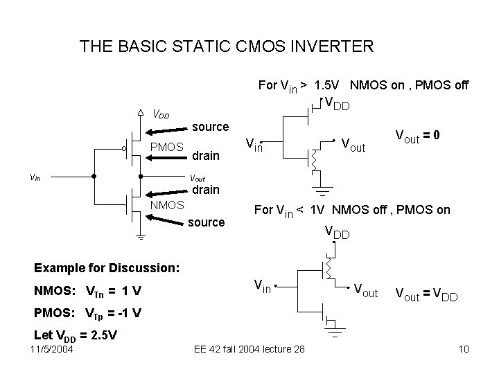
THE BASIC STATIC CMOS INVERTER VDD PMOS vin For Vin > 1. 5 V NMOS on , PMOS off VDD source drain Vout = 0 vout drain NMOS source For Vin < 1 V NMOS off , PMOS on VDD Example for Discussion: NMOS: VTn = 1 V Vin Vout = VDD PMOS: VTp = -1 V Let VDD = 2. 5 V 11/5/2004 EE 42 fall 2004 lecture 28 10

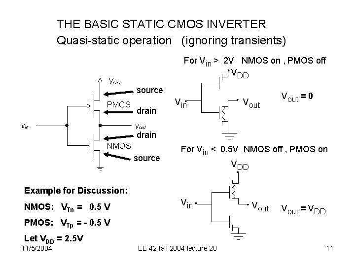
THE BASIC STATIC CMOS INVERTER Quasi-static operation (ignoring transients) VDD PMOS vin For Vin > 2 V NMOS on , PMOS off VDD source drain Vout = 0 vout drain NMOS source For Vin < 0. 5 V NMOS off , PMOS on VDD Example for Discussion: NMOS: VTn = 0. 5 V Vin Vout = VDD PMOS: VTp = - 0. 5 V Let VDD = 2. 5 V 11/5/2004 EE 42 fall 2004 lecture 28 11

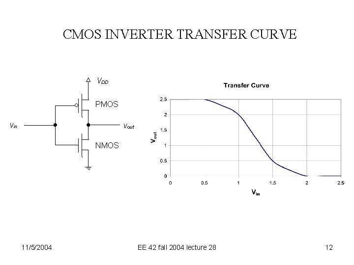
CMOS INVERTER TRANSFER CURVE VDD PMOS vin vout NMOS 11/5/2004 EE 42 fall 2004 lecture 28 12

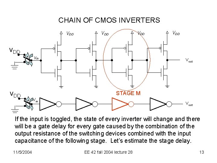
CHAIN OF CMOS INVERTERS VDD VDD VDD vin VDD Vout STAGE M Vin Vout If the input is toggled, the state of every inverter will change and there will be a gate delay for every gate caused by the combination of the output resistance of the switching devices combined with the input capacitance of the following stage. Let’s estimate the stage delay. 11/5/2004 EE 42 fall 2004 lecture 28 13

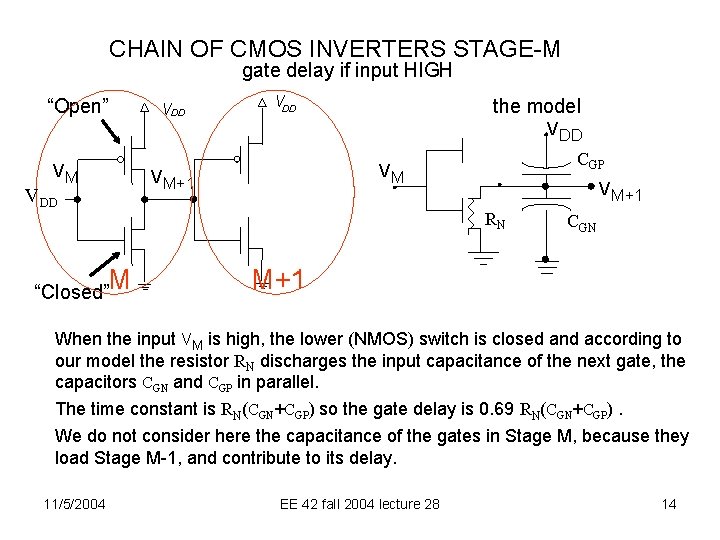
CHAIN OF CMOS INVERTERS STAGE-M gate delay if input HIGH “Open” VDD the model VDD VM VM+1 VDD CGP VM VM+1 RN M “Closed” CGN M+1 When the input VM is high, the lower (NMOS) switch is closed and according to our model the resistor RN discharges the input capacitance of the next gate, the capacitors CGN and CGP in parallel. The time constant is RN(CGN+CGP) so the gate delay is 0. 69 RN(CGN+CGP). We do not consider here the capacitance of the gates in Stage M, because they load Stage M-1, and contribute to its delay. 11/5/2004 EE 42 fall 2004 lecture 28 14

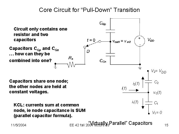
Core Circuit for “Pull-Down” Transition Circuit only contains one resistor and two capacitors CGp and CGn … how can they be combined into one? V 2= VDD Capacitors share one node; the other nodes are held at constant voltages. i(t) KCL: currents sum at common node, ie node capacitance is SUM (parallel capacitor formula). 11/5/2004 “Virtually EE 42 fall 2004 lecture 28 Parallel” C 2 i 2(t) v. C(t) i 1(t) C 1 V 1= 0 Capacitors 15

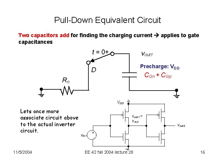
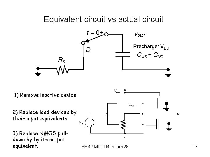
Pull-Down Equivalent Circuit Two capacitors add for finding the charging current applies to gate capacitances t = 0+ vout 1 Precharge: VDD D CGn + CGp Rn VDD Lets once more associate circuit above to the actual inverter circuit. 11/5/2004 vout 1 = v in 2 vin 1 vout 2 + - EE 42 fall 2004 lecture 28 16

Equivalent circuit vs actual circuit t = 0+ vout 1 Precharge: VDD D CGn + CGp Rn VDD 1) Remove inactive device 2) Replace load devices by their input equivalents 3) Replace NMOS pulldown by by its output equivalent. 11/5/2004 vout 1 v in 2 vin 1 vout 2 + - EE 42 fall 2004 lecture 28 17

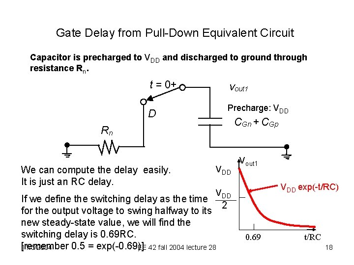
Gate Delay from Pull-Down Equivalent Circuit Capacitor is precharged to VDD and discharged to ground through resistance Rn. t = 0+ vout 1 Precharge: VDD D CGn + CGp Rn We can compute the delay easily. It is just an RC delay. VDD Vout 1 VDD exp(-t/RC) VDD If we define the switching delay as the time 2 for the output voltage to swing halfway to its new steady-state value, we will find the switching delay is 0. 69 RC. [remember 0. 5 = exp(-0. 69)] 11/5/2004 EE 42 fall 2004 lecture 28 0. 69 t/RC 18

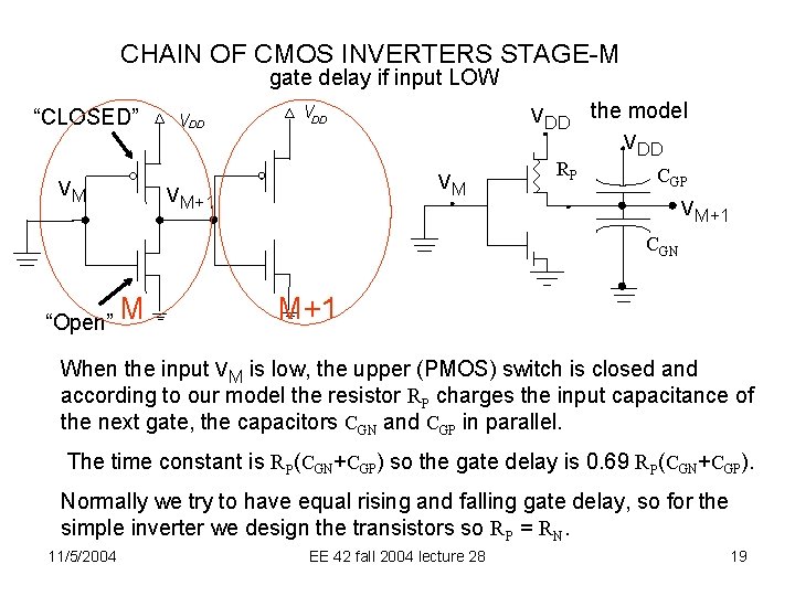
CHAIN OF CMOS INVERTERS STAGE-M gate delay if input LOW “CLOSED” VM VDD VDD VM VM+1 RP the model VDD CGP VM+1 CGN “Open” M M+1 When the input VM is low, the upper (PMOS) switch is closed and according to our model the resistor RP charges the input capacitance of the next gate, the capacitors CGN and CGP in parallel. The time constant is RP(CGN+CGP) so the gate delay is 0. 69 RP(CGN+CGP). Normally we try to have equal rising and falling gate delay, so for the simple inverter we design the transistors so RP = RN. 11/5/2004 EE 42 fall 2004 lecture 28 19

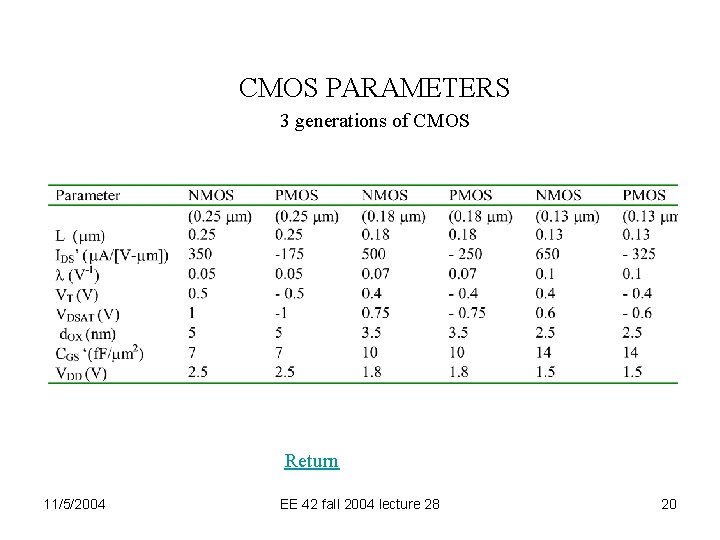
CMOS PARAMETERS 3 generations of CMOS Return 11/5/2004 EE 42 fall 2004 lecture 28 20

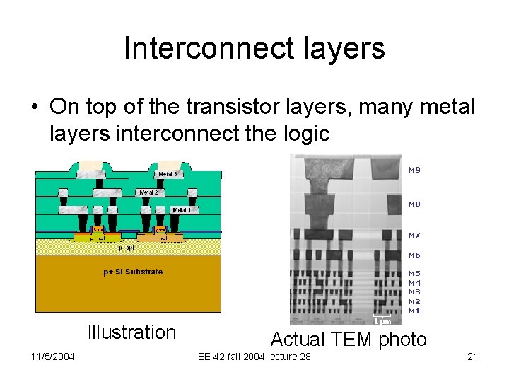
Interconnect layers • On top of the transistor layers, many metal layers interconnect the logic Illustration 11/5/2004 Actual TEM photo EE 42 fall 2004 lecture 28 21

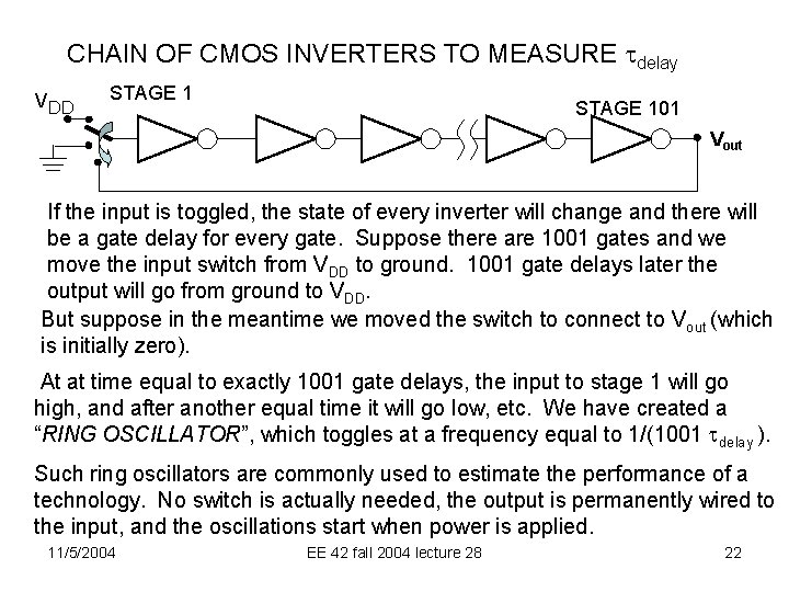
CHAIN OF CMOS INVERTERS TO MEASURE tdelay VDD STAGE 101 Vout If the input is toggled, the state of every inverter will change and there will be a gate delay for every gate. Suppose there are 1001 gates and we move the input switch from VDD to ground. 1001 gate delays later the output will go from ground to VDD. But suppose in the meantime we moved the switch to connect to Vout (which is initially zero). At at time equal to exactly 1001 gate delays, the input to stage 1 will go high, and after another equal time it will go low, etc. We have created a “RING OSCILLATOR”, which toggles at a frequency equal to 1/(1001 tdelay ). Such ring oscillators are commonly used to estimate the performance of a technology. No switch is actually needed, the output is permanently wired to the input, and the oscillations start when power is applied. 11/5/2004 EE 42 fall 2004 lecture 28 22

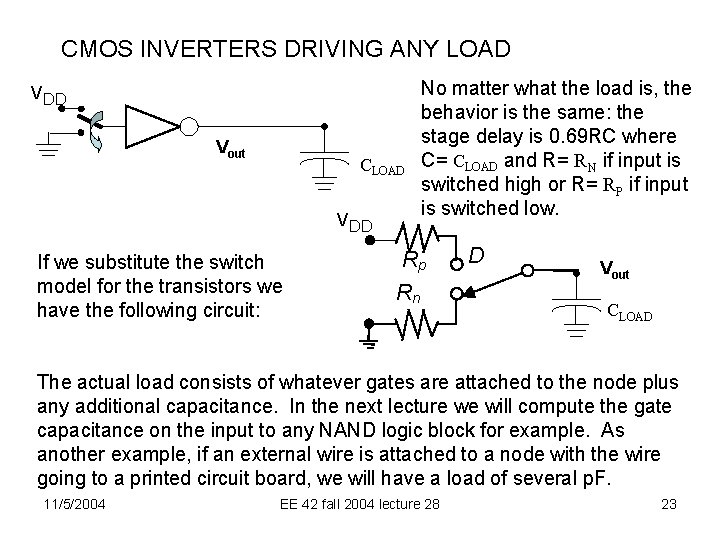
CMOS INVERTERS DRIVING ANY LOAD VDD Vout CLOAD VDD If we substitute the switch model for the transistors we have the following circuit: No matter what the load is, the behavior is the same: the stage delay is 0. 69 RC where C= CLOAD and R= RN if input is switched high or R= RP if input is switched low. Rp Rn D Vout CLOAD The actual load consists of whatever gates are attached to the node plus any additional capacitance. In the next lecture we will compute the gate capacitance on the input to any NAND logic block for example. As another example, if an external wire is attached to a node with the wire going to a printed circuit board, we will have a load of several p. F. 11/5/2004 EE 42 fall 2004 lecture 28 23