
ENEE 303 3 rd Discussion Contents MOSFET small


- Slides: 18
ENEE 303 3 rd Discussion
Contents • MOSFET small signal equivalent circuit • BJT small signal equivalent circuit
MOSFET: Small-Signal Equivalent Circuit Y admittance matrix • Small-signal models for the MOSFET: (a) neglecting the dependence of i. D on v. DS in saturation (the channel-length modulation effect) and (b) including the effect of channel length modulation ENEE 303 Fall 2017
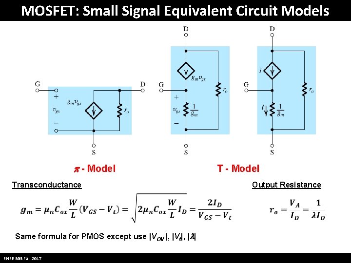
MOSFET: Small Signal Equivalent Circuit Models p - Model Transconductance Same formula for PMOS except use |VOV |, |Vt|, |l| ENEE 303 Fall 2017 T - Model Output Resistance
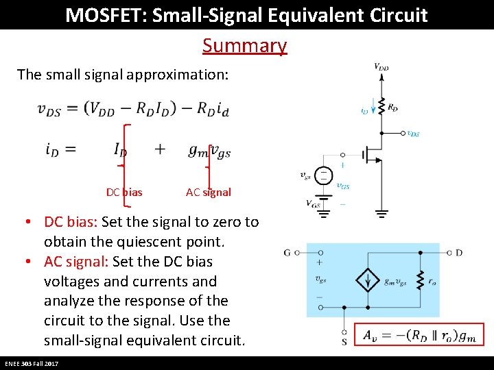
MOSFET: Small-Signal Equivalent Circuit Summary The small signal approximation: DC bias AC signal • DC bias: Set the signal to zero to obtain the quiescent point. • AC signal: Set the DC bias voltages and currents and analyze the response of the circuit to the signal. Use the small-signal equivalent circuit. ENEE 303 Fall 2017
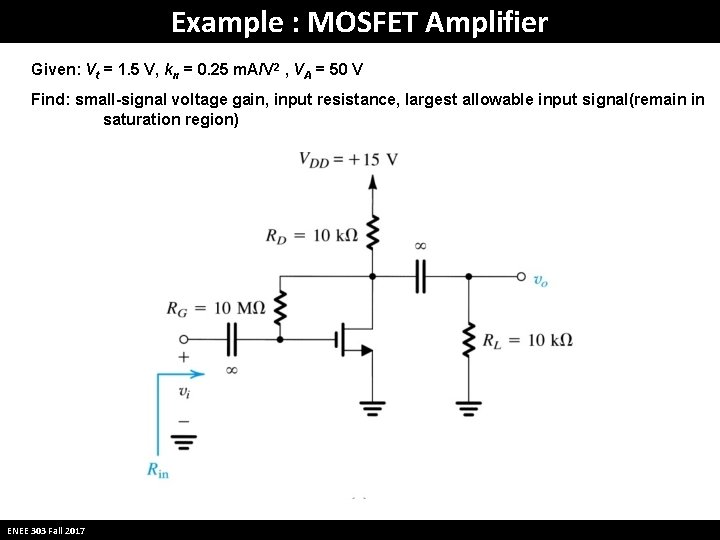
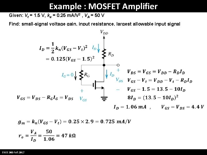
Example : MOSFET Amplifier Given: Vt = 1. 5 V, kn = 0. 25 m. A/V 2 , VA = 50 V Find: small-signal voltage gain, input resistance, largest allowable input signal(remain in saturation region) ENEE 303 Fall 2017
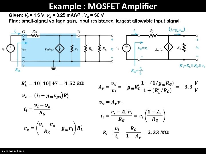
Example : MOSFET Amplifier Given: Vt = 1. 5 V, kn = 0. 25 m. A/V 2 , VA = 50 V Find: small-signal voltage gain, input resistance, largest allowable input signal ENEE 303 Fall 2017
Example : MOSFET Amplifier Given: Vt = 1. 5 V, kn = 0. 25 m. A/V 2 , VA = 50 V Find: small-signal voltage gain, input resistance, largest allowable input signal ENEE 303 Fall 2017
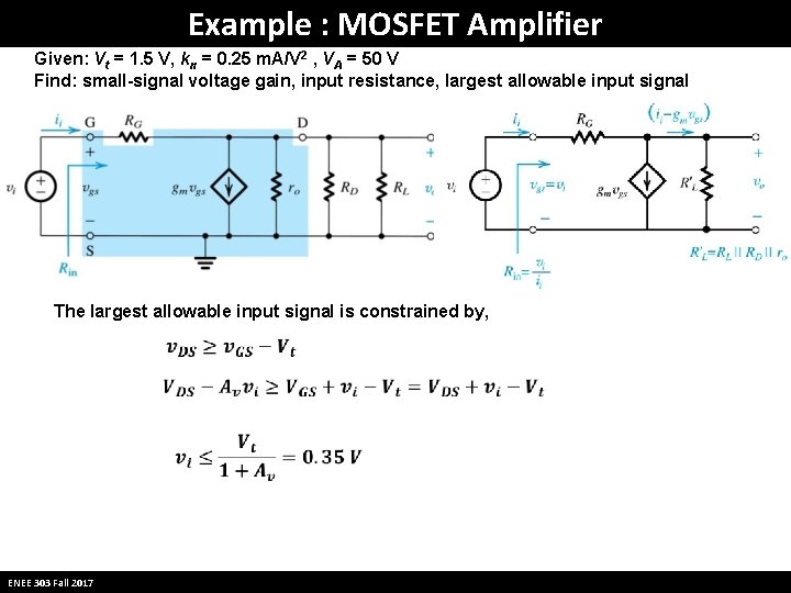
Example : MOSFET Amplifier Given: Vt = 1. 5 V, kn = 0. 25 m. A/V 2 , VA = 50 V Find: small-signal voltage gain, input resistance, largest allowable input signal The largest allowable input signal is constrained by, ENEE 303 Fall 2017
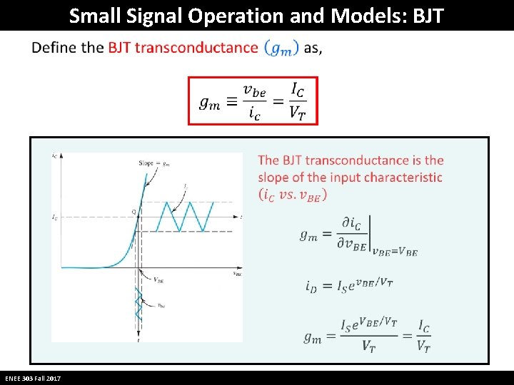
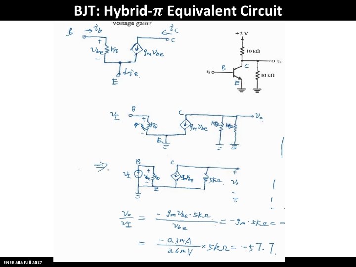
Small Signal Operation and Models: BJT ENEE 303 Fall 2017
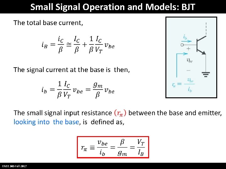
Small Signal Operation and Models: BJT The total base current, The signal current at the base is then, ENEE 303 Fall 2017
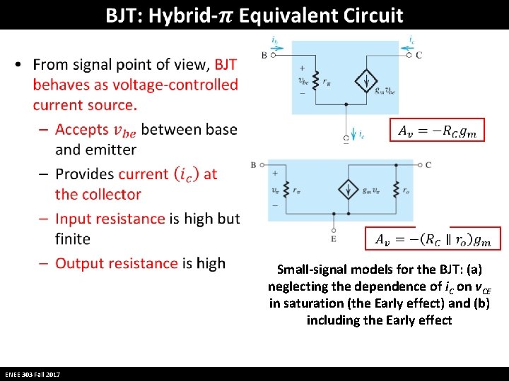
• Small-signal models for the BJT: (a) neglecting the dependence of i. C on v. CE in saturation (the Early effect) and (b) including the Early effect ENEE 303 Fall 2017
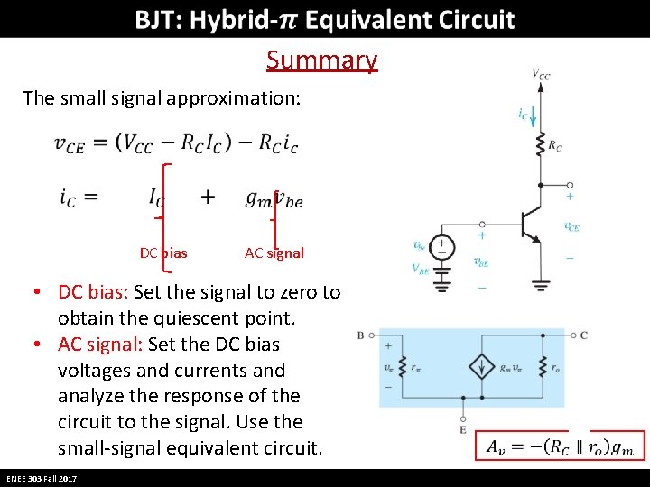
Summary The small signal approximation: DC bias AC signal • DC bias: Set the signal to zero to obtain the quiescent point. • AC signal: Set the DC bias voltages and currents and analyze the response of the circuit to the signal. Use the small-signal equivalent circuit. ENEE 303 Fall 2017
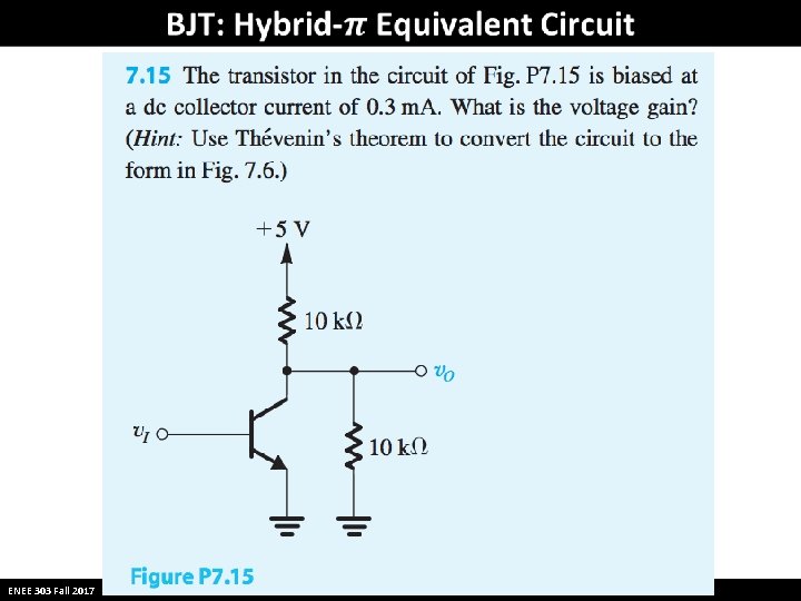
ENEE 303 Fall 2017
ENEE 303 Fall 2017
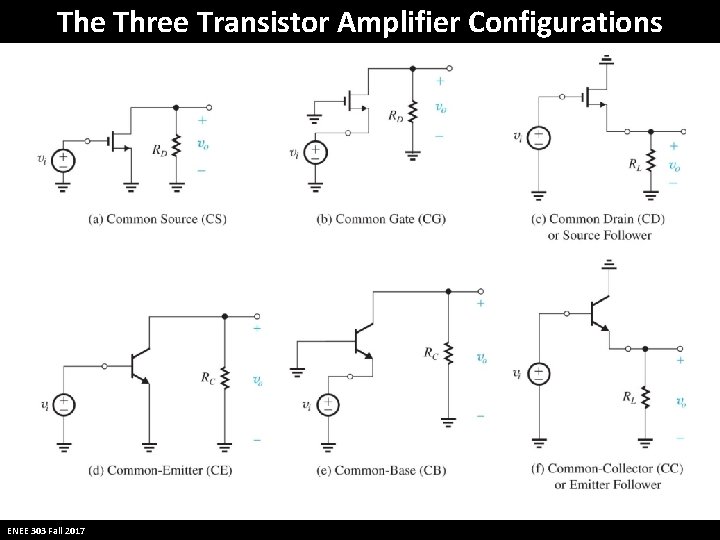
The Three Transistor Amplifier Configurations ENEE 303 Fall 2017
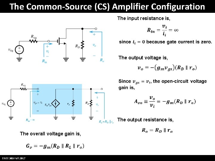
The Common-Source (CS) Amplifier Configuration The input resistance is, The output voltage is, The output resistance is, The overall voltage gain is, ENEE 303 Fall 2017
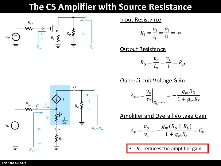
The CS Amplifier with Source Resistance Input Resistance Output Resistance Open-Circuit Voltage Gain Amplifier and Overall Voltage Gain ENEE 303 Fall 2017