Lecture 17 Today we will discuss p Metal
- Slides: 20

Lecture 17 Today we will discuss p Metal Oxide Semiconductor (MOS) Transistors n n n Physical structure Physical operation Circuit symbol and current/voltage designations Modes of operation I-V Relationship Solution of MOS circuits

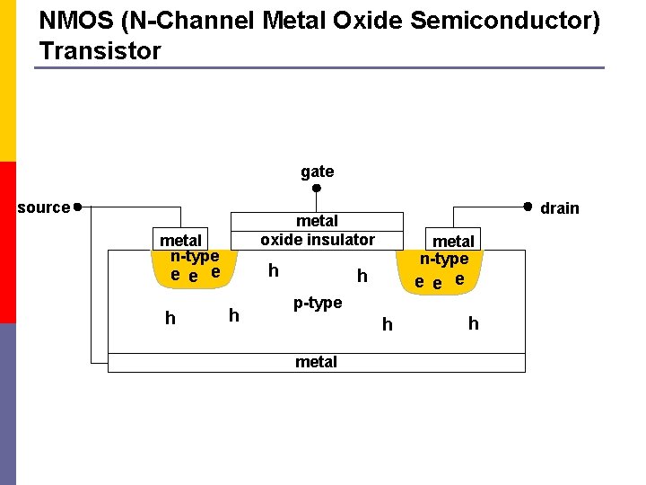
NMOS (N-Channel Metal Oxide Semiconductor) Transistor gate source metal n-type h e e e h drain metal oxide insulator h metal n-type h e e e p-type h metal h

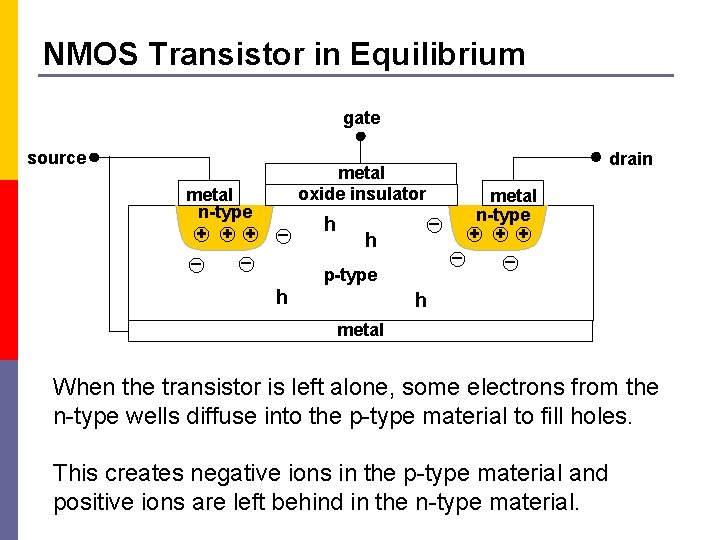
NMOS Transistor in Equilibrium gate source metal n-type + + + _ _ metal oxide insulator _ h h drain metal _ n-type + + + _ _ p-type h h metal When the transistor is left alone, some electrons from the n-type wells diffuse into the p-type material to fill holes. This creates negative ions in the p-type material and positive ions are left behind in the n-type material.

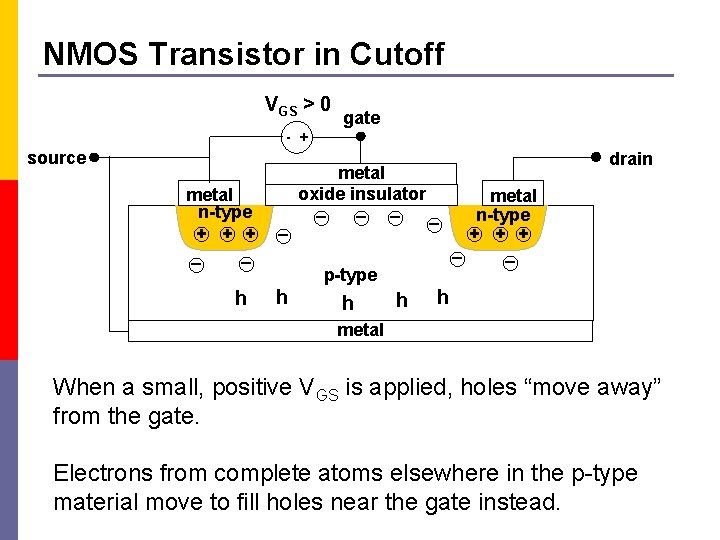
NMOS Transistor in Cutoff VGS > 0 gate - + source metal n-type + + + _ _ h _ metal oxide insulator _ _ drain metal n-type + + + _ _ p-type h h metal When a small, positive VGS is applied, holes “move away” from the gate. Electrons from complete atoms elsewhere in the p-type material move to fill holes near the gate instead.

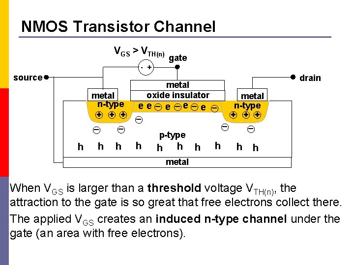
NMOS Transistor Channel VGS > VTH(n) gate - + source metal n-type + + + _ _ h h h metal oxide insulator ee_ e _ _ drain metal n-type + + + _ _ p-type h h h h metal When VGS is larger than a threshold voltage VTH(n), the attraction to the gate is so great that free electrons collect there. The applied VGS creates an induced n-type channel under the gate (an area with free electrons).

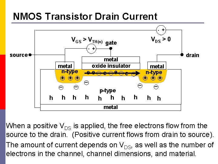
NMOS Transistor Drain Current - + VGS > VTH(n) VDS > 0 gate - + source metal n-type + + + _ _ h h h metal oxide insulator ee_ e _ _ drain metal n-type + + + _ _ p-type h h h h metal When a positive VDS is applied, the free electrons flow from the source to the drain. (Positive current flows from drain to source). The amount of current depends on VDS, as well as the number of electrons in the channel, channel dimensions, and material.

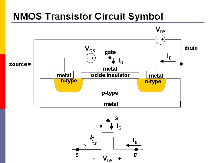
NMOS Transistor Circuit Symbol VDS - + VGS drain gate - + source ID IG metal oxide insulator metal n-type p-type metal G + _ S IG V ID GS - VDS + D

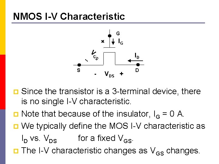
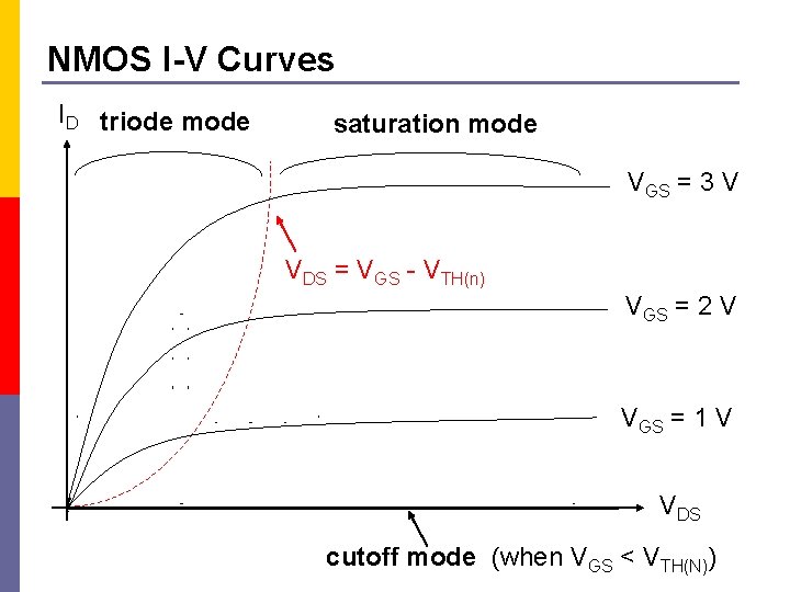
NMOS I-V Characteristic G + _ S IG V ID GS - VDS + D Since the transistor is a 3 -terminal device, there is no single I-V characteristic. p Note that because of the insulator, IG = 0 A. p We typically define the MOS I-V characteristic as ID vs. VDS for a fixed VGS. p The I-V characteristic changes as VGS changes. p

NMOS I-V Curves ID triode mode saturation mode VGS = 3 V VDS = VGS - VTH(n) VGS = 2 V VGS = 1 V VDS cutoff mode (when VGS < VTH(N))

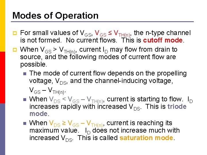
Modes of Operation p p For small values of VGS, VGS ≤ VTH(n), the n-type channel is not formed. No current flows. This is cutoff mode. When VGS > VTH(n), current ID may flow from drain to source, and the following modes of current flow are possible. n The mode of current flow depends on the propelling voltage, VDS, and the channel-inducing voltage, VGS – VTH(n). n When VDS < VGS – VTH(n), current is starting to flow. ID increases rapidly with increased VDS. This is triode mode. n When VDS ≥ VGS – VTH(n), current is reaching its maximum value. ID does not increase much with increased VDS. This is called saturation mode.

Faucet Analogy Imagine the faucet on your kitchen sink. p To make water flow, the water supply has to be connected to the faucet. This establishes a path for water to flow. p Setting VGS above threshold voltage is like connecting the water supply. p Cutoff = water supply disconnected (no path for current flow) p Setting VGS to a larger value is like connecting a high -pressure water supply—more flow can potentially occur.

Faucet Analogy The faucet itself is used to adjust water flow. You can turn the flow up and down. p VDS is like the faucet. It controls the amount of flow. p There is, of course, a saturation point. If you keep turning the faucet control, eventually you won’t get any more flow. p Triode = faucet in “normal range”, controls flow p Saturation = faucet turned up to (or past) point for maximum flow p

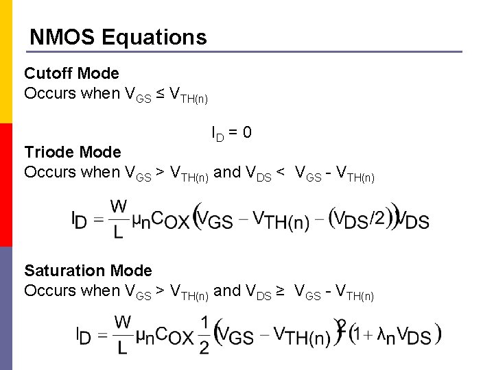
NMOS Equations Cutoff Mode Occurs when VGS ≤ VTH(n) ID = 0 Triode Mode Occurs when VGS > VTH(n) and VDS < VGS - VTH(n) Saturation Mode Occurs when VGS > VTH(n) and VDS ≥ VGS - VTH(n)

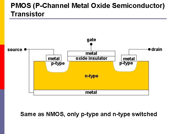
PMOS (P-Channel Metal Oxide Semiconductor) Transistor gate source metal p-type metal oxide insulator drain metal p-type n-type metal Same as NMOS, only p-type and n-type switched

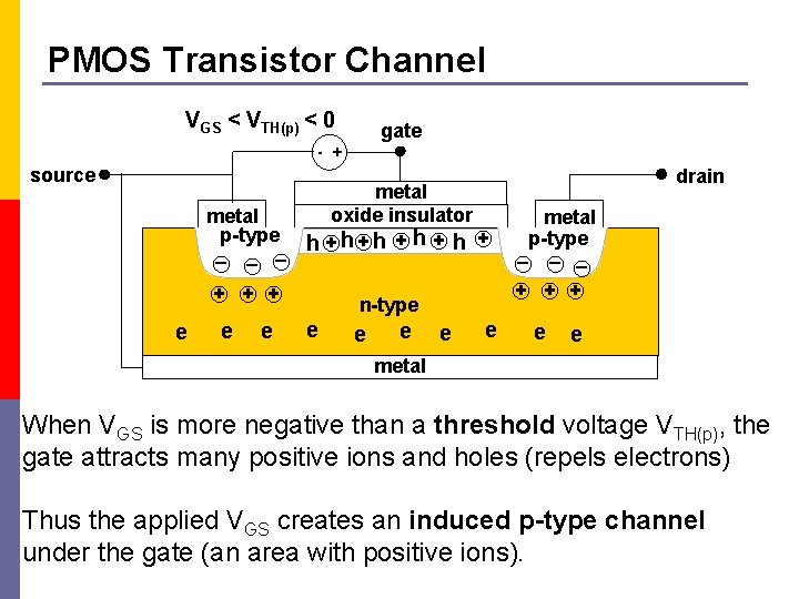
PMOS Transistor Channel VGS < VTH(p) < 0 gate - + source metal p-type _ _ _ metal oxide insulator h +h+h + h + + e e e metal p-type _ _ _ + + + n-type e drain e e metal When VGS is more negative than a threshold voltage VTH(p), the gate attracts many positive ions and holes (repels electrons) Thus the applied VGS creates an induced p-type channel under the gate (an area with positive ions).

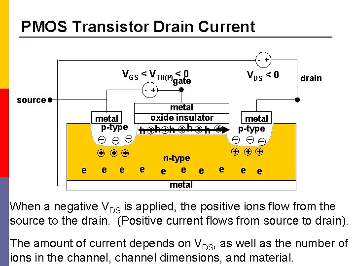
PMOS Transistor Drain Current - + VGS < VTH(P) < 0 VDS < 0 gate drain - + source metal p-type _ _ _ metal oxide insulator h +h+h + h + + e e e + + + n-type e metal p-type _ _ _ e e metal When a negative VDS is applied, the positive ions flow from the source to the drain. (Positive current flows from source to drain). The amount of current depends on VDS, as well as the number of ions in the channel, channel dimensions, and material.

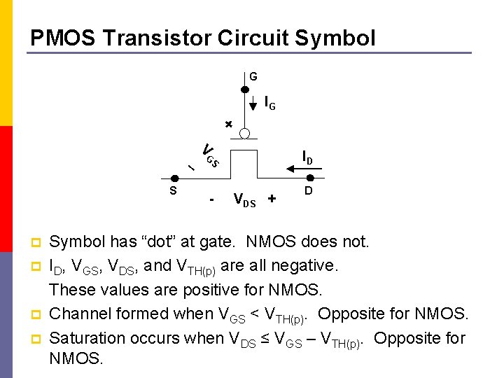
PMOS Transistor Circuit Symbol G IG + _ S p p V ID GS - VDS + D Symbol has “dot” at gate. NMOS does not. ID, VGS, VDS, and VTH(p) are all negative. These values are positive for NMOS. Channel formed when VGS < VTH(p). Opposite for NMOS. Saturation occurs when VDS ≤ VGS – VTH(p). Opposite for NMOS.

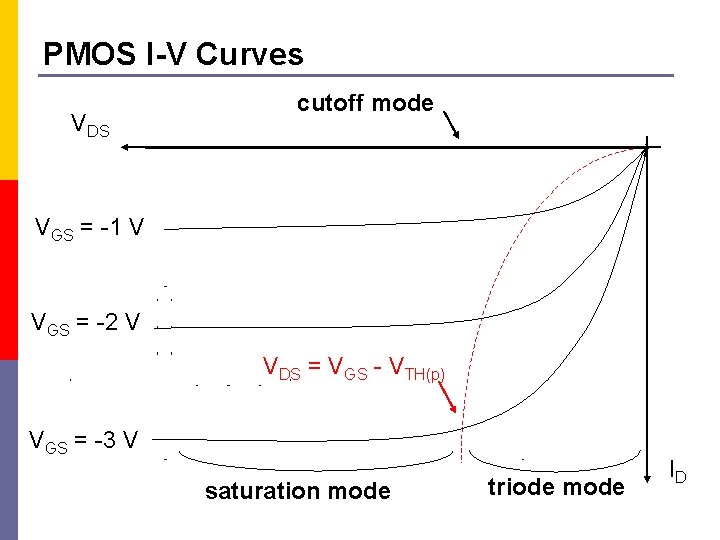
PMOS I-V Curves VDS cutoff mode VGS = -1 V VGS = -2 V VDS = VGS - VTH(p) VGS = -3 V saturation mode triode mode ID

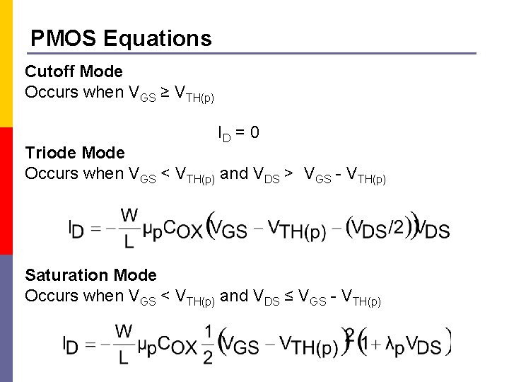
PMOS Equations Cutoff Mode Occurs when VGS ≥ VTH(p) ID = 0 Triode Mode Occurs when VGS < VTH(p) and VDS > VGS - VTH(p) Saturation Mode Occurs when VGS < VTH(p) and VDS ≤ VGS - VTH(p)

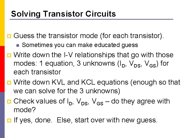
Solving Transistor Circuits p Guess the transistor mode (for each transistor). n Sometimes you can make educated guess Write down the I-V relationships that go with those modes: 1 equation, 3 unknowns (ID, VDS, VGS) for each transistor p Write down KVL and KCL equations (enough so that we can solve for the 3 unknowns) p Check values of ID, VDS, VGS – do they agree with mode? p If yes, done. Else, start over with new guess. p