Institut de recherche sur les lois fondamentales de



- Slides: 66

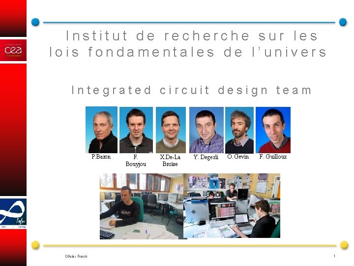
Institut de recherche sur les lois fondamentales de l’univers Integrated circuit design team P. Baron Olivier Gevin F. Bouyjou X. De-La Broïse Y. Degerli O. Gevin F. Guilloux 1

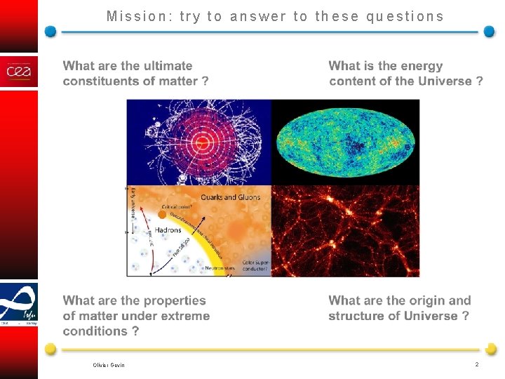
Mission: try to answer to these questions Olivier Gevin 2

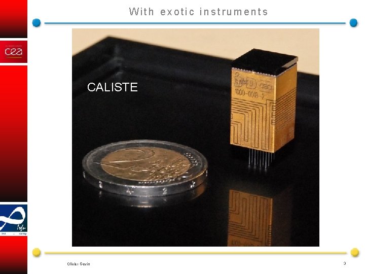
With exotic instruments CALISTE Olivier Gevin 3

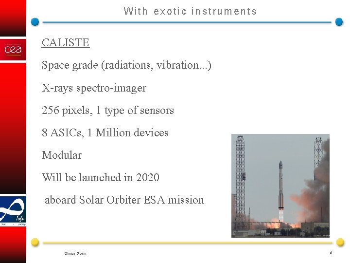
With exotic instruments CALISTE Space grade (radiations, vibration. . . ) X-rays spectro-imager 256 pixels, 1 type of sensors 8 ASICs, 1 Million devices Modular Will be launched in 2020 aboard Solar Orbiter ESA mission Olivier Gevin 4

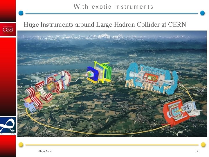
With exotic instruments Huge Instruments around Large Hadron Collider at CERN Olivier Gevin 5

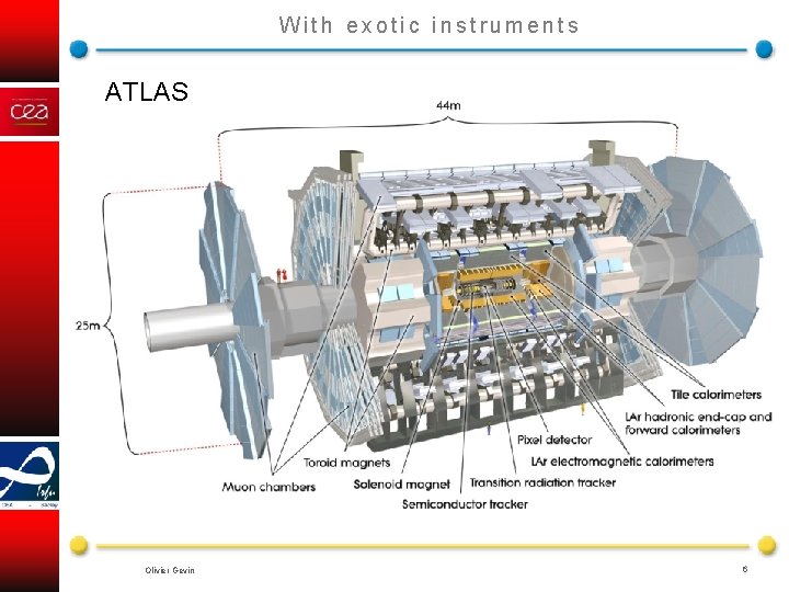
With exotic instruments ATLAS Olivier Gevin 6

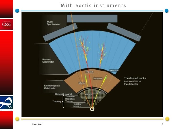
With exotic instruments Olivier Gevin 7

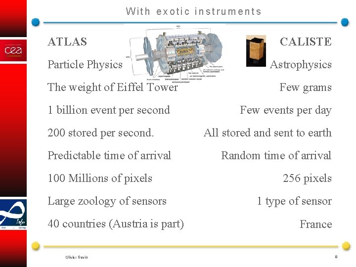
With exotic instruments ATLAS Particle Physics The weight of Eiffel Tower 1 billion event per second 200 stored per second. Predictable time of arrival 100 Millions of pixels Large zoology of sensors 40 countries (Austria is part) Olivier Gevin CALISTE Astrophysics Few grams Few events per day All stored and sent to earth Random time of arrival 256 pixels 1 type of sensor France 8

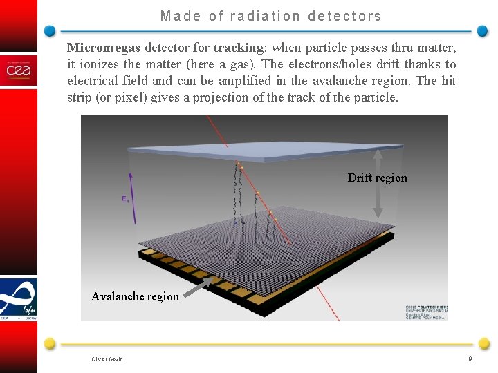
Made of radiation detectors Micromegas detector for tracking: when particle passes thru matter, it ionizes the matter (here a gas). The electrons/holes drift thanks to electrical field and can be amplified in the avalanche region. The hit strip (or pixel) gives a projection of the track of the particle. Drift region Avalanche region Olivier Gevin 9

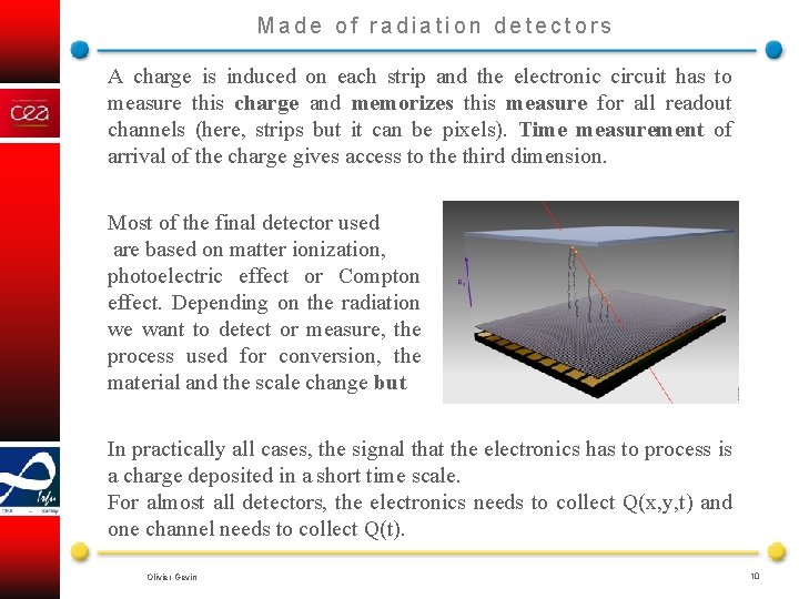
Made of radiation detectors A charge is induced on each strip and the electronic circuit has to measure this charge and memorizes this measure for all readout channels (here, strips but it can be pixels). Time measurement of arrival of the charge gives access to the third dimension. Most of the final detector used are based on matter ionization, photoelectric effect or Compton effect. Depending on the radiation we want to detect or measure, the process used for conversion, the material and the scale change but In practically all cases, the signal that the electronics has to process is a charge deposited in a short time scale. For almost all detectors, the electronics needs to collect Q(x, y, t) and one channel needs to collect Q(t). Olivier Gevin 10

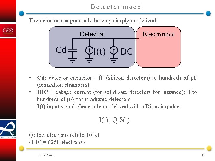
Detector model The detector can generally be very simply modelized: Detector Electronics • Cd: detector capacitor: f. F (silicon detectors) to hundreds of p. F (ionization chambers) • IDC: Leakage current (for solid sate detectors for instance): 0 to hundreds of µA for irradiated detectors. • I(t) input signal. Generally modelized with a Dirac impulse: I(t)=Q. d(t) Q: few electrons (el) to 106 el (1 f. C = 6250 electrons) Olivier Gevin 11

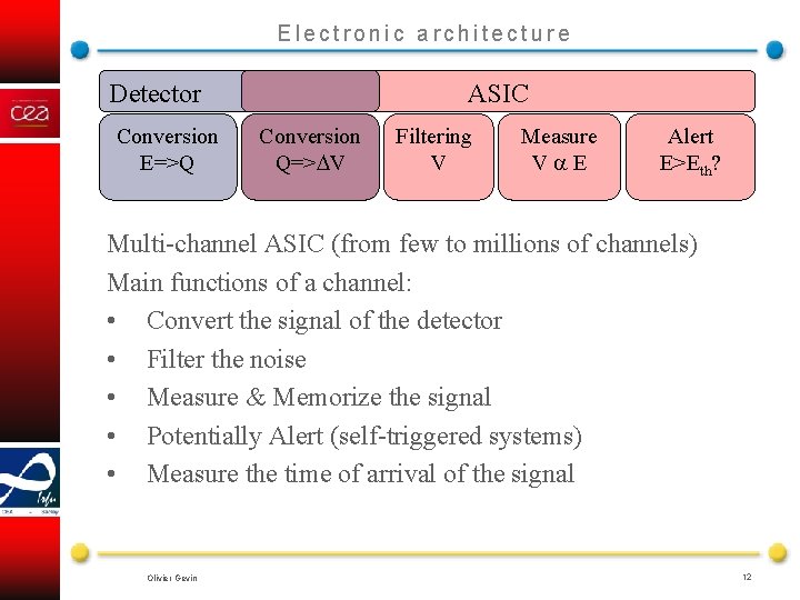
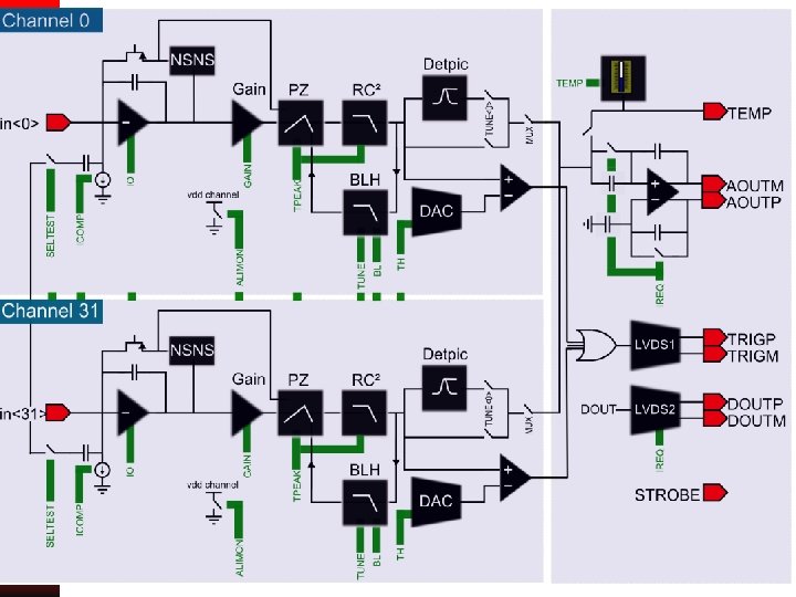
Electronic architecture Detector Conversion E=>Q ASIC Conversion Q=> V Filtering V Measure V E Alert E>Eth? Multi-channel ASIC (from few to millions of channels) Main functions of a channel: • Convert the signal of the detector • Filter the noise • Measure & Memorize the signal • Potentially Alert (self-triggered systems) • Measure the time of arrival of the signal Olivier Gevin 12

Electronic architecture Detector Conversion E=>Q ASIC Conversion Q=> V Filtering V Measure V E Alert E>Eth? Multi-channel ASIC (from few to millions of channels) Main functions of a channel: • Convert the signal of the detector • Filter the noise • Measure & Memorize the signal • Potentially Alert (self-triggered systems) • Measure the time of arrival of the signal Olivier Gevin 13

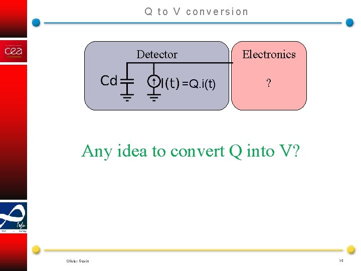
Q to V conversion Electronics Detector =Q. i(t) ? Any idea to convert Q into V? Olivier Gevin 14

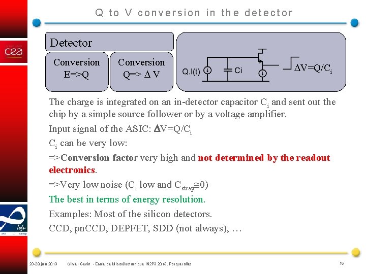
Q to V conversion in the detector Detector Conversion E=>Q Conversion Q=> V V=Q/Ci The charge is integrated on an in-detector capacitor Ci and sent out the chip by a simple source follower or by a voltage amplifier. Input signal of the ASIC: V=Q/Ci Ci can be very low: =>Conversion factor very high and not determined by the readout electronics. =>Very low noise (Ci low and Cstray 0) The best in terms of energy resolution. Examples: Most of the silicon detectors. CCD, pn. CCD, DEPFET, SDD (not always), … 23 -28 juin 2013 Olivier Gevin -Ecole de Microélectronique IN 2 P 3 2013, Porquerolles 15

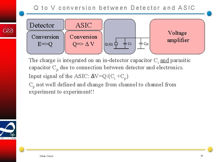
Q to V conversion between Detector and ASIC Detector Conversion E=>Q ASIC Conversion Q=> V Voltage amplifier The charge is integrated on an in-detector capacitor Ci and parasitic capacitor Cp due to connection between detector and electronics. Input signal of the ASIC: V=Q/(Ci +Cp) Cp not well defined and change from channel to channel from experiment to experiment!! Olivier Gevin 16

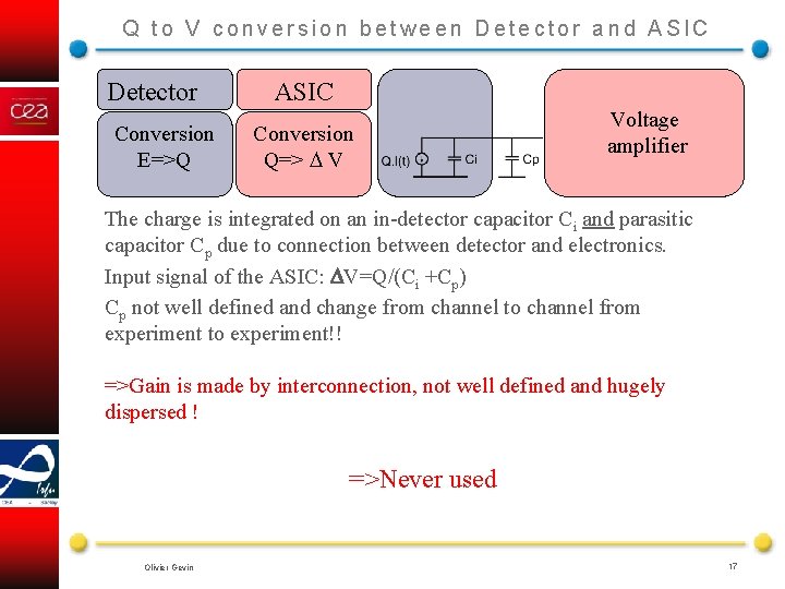
Q to V conversion between Detector and ASIC Detector Conversion E=>Q ASIC Conversion Q=> V Voltage amplifier The charge is integrated on an in-detector capacitor Ci and parasitic capacitor Cp due to connection between detector and electronics. Input signal of the ASIC: V=Q/(Ci +Cp) Cp not well defined and change from channel to channel from experiment to experiment!! =>Gain is made by interconnection, not well defined and hugely dispersed ! =>Never used Olivier Gevin 17

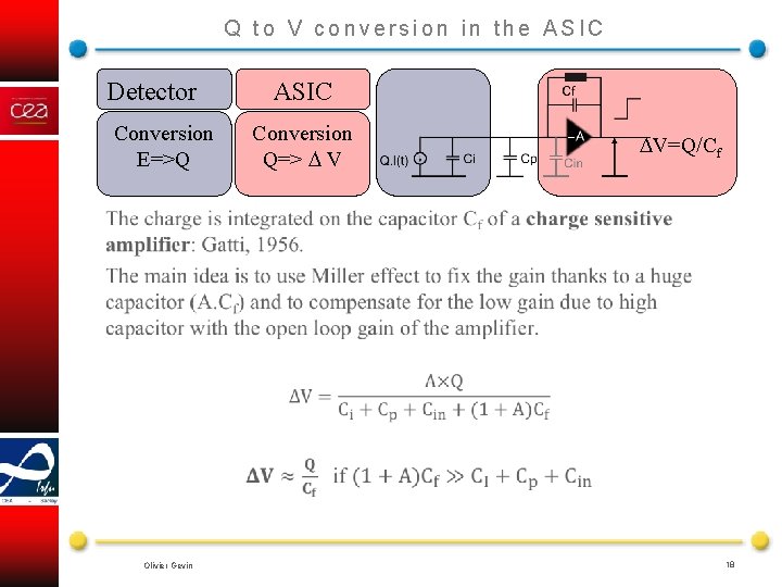
Q to V conversion in the ASIC Detector Conversion E=>Q ASIC Conversion Q=> V V=Q/Cf Olivier Gevin 18

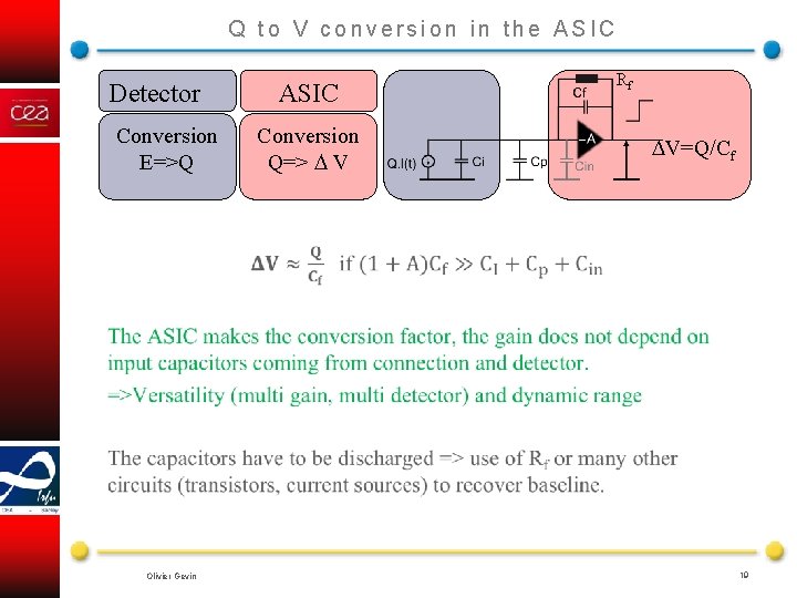
Q to V conversion in the ASIC Detector Conversion E=>Q ASIC Conversion Q=> V Rf V=Q/Cf Olivier Gevin 19

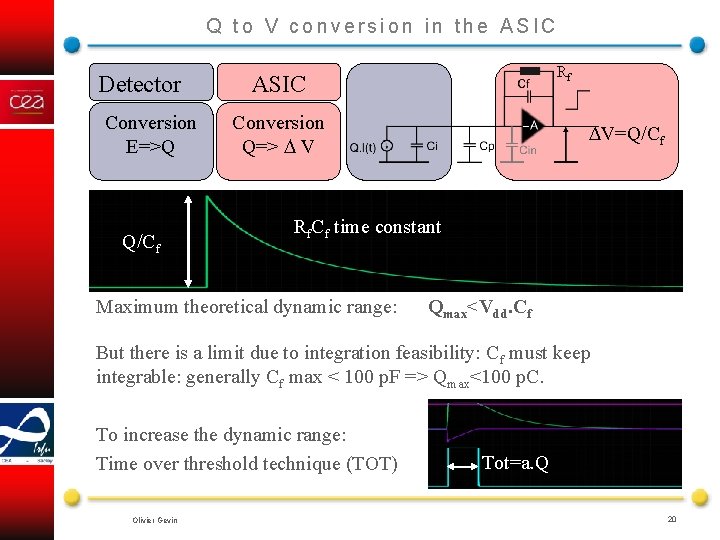
Q to V conversion in the ASIC Detector Conversion E=>Q Q/Cf ASIC Rf Conversion Q=> V V=Q/Cf Rf. Cf time constant Maximum theoretical dynamic range: Qmax<Vdd. Cf But there is a limit due to integration feasibility: Cf must keep integrable: generally Cf max < 100 p. F => Qmax<100 p. C. To increase the dynamic range: Time over threshold technique (TOT) Olivier Gevin Tot=a. Q 20

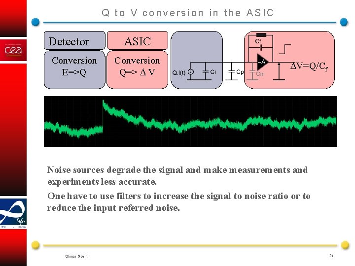
Q to V conversion in the ASIC Detector Conversion E=>Q ASIC Conversion Q=> V V=Q/Cf Noise sources degrade the signal and make measurements and experiments less accurate. One have to use filters to increase the signal to noise ratio or to reduce the input referred noise. Olivier Gevin 21

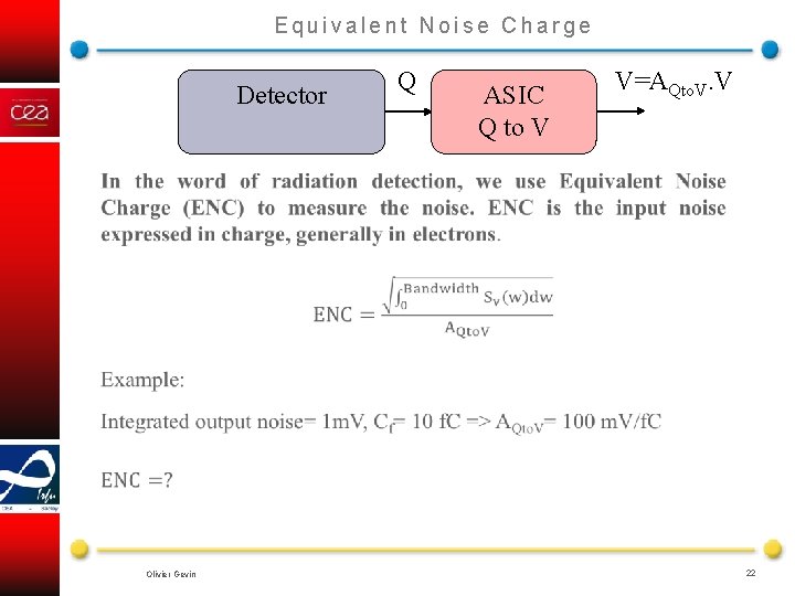
Equivalent Noise Charge Detector Olivier Gevin Q ASIC Q to V V=AQto. V. V 22

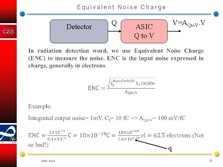
Equivalent Noise Charge Detector Q V=AQto. V. V ASIC Q to V q Olivier Gevin 23

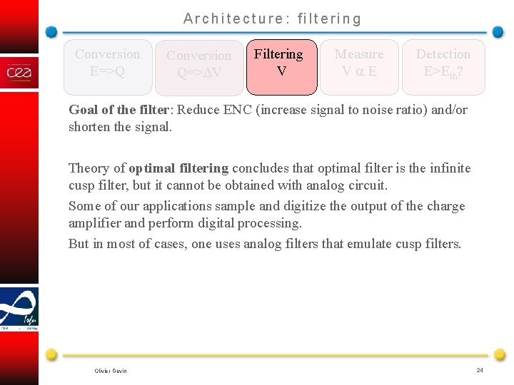
Architecture: filtering Conversion E=>Q Conversion Q=> V Filtering V Measure V E Detection E>Eth? Goal of the filter: Reduce ENC (increase signal to noise ratio) and/or shorten the signal. Theory of optimal filtering concludes that optimal filter is the infinite cusp filter, but it cannot be obtained with analog circuit. Some of our applications sample and digitize the output of the charge amplifier and perform digital processing. But in most of cases, one uses analog filters that emulate cusp filters. Olivier Gevin 24

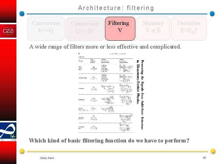
Architecture: filtering Conversion E=>Q Conversion Q=> V Filtering V Measure V E Detection E>Eth? A wide range of filters more or less effective and complicated. Which kind of basic filtering function do we have to perform? Olivier Gevin 25

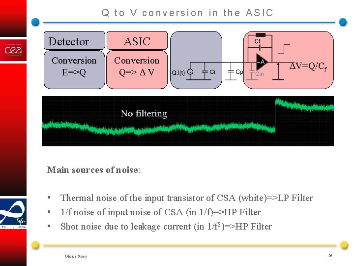
Q to V conversion in the ASIC Detector Conversion E=>Q ASIC Conversion Q=> V V=Q/Cf Main sources of noise: • Thermal noise of the input transistor of CSA (white)=>LP Filter • 1/f noise of input noise of CSA (in 1/f)=>HP Filter • Shot noise due to leakage current (in 1/f 2)=>HP Filter Olivier Gevin 26

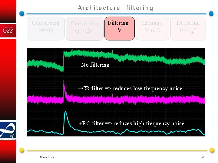
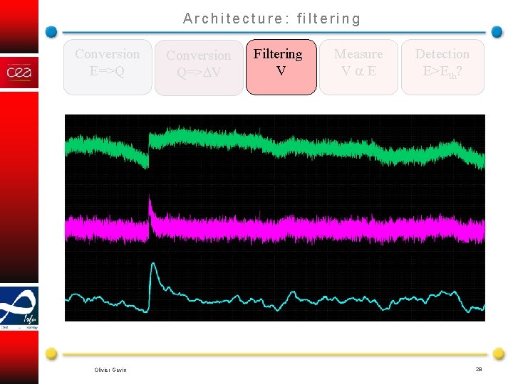
Architecture: filtering Conversion E=>Q Conversion Q=> V Filtering V Measure V E Detection E>Eth? No filtering +CR filter => reduces low frequency noise +RC filter => reduces high frequency noise Olivier Gevin 27

Architecture: filtering Conversion E=>Q Olivier Gevin Conversion Q=> V Filtering V Measure V E Detection E>Eth? 28

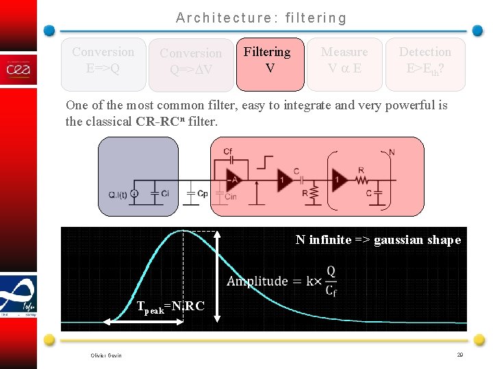
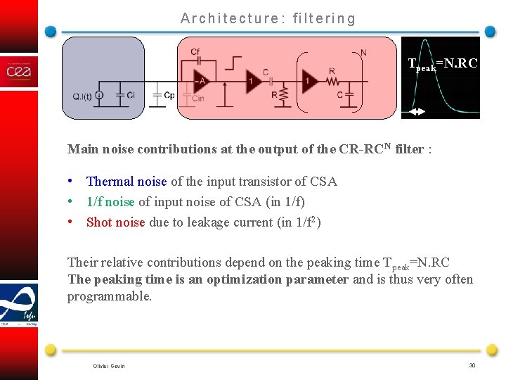
Architecture: filtering Conversion E=>Q Filtering V Conversion Q=> V Measure V E Detection E>Eth? One of the most common filter, easy to integrate and very powerful is the classical CR-RCn filter. N infinite => gaussian shape Tpeak=N. RC Olivier Gevin 29

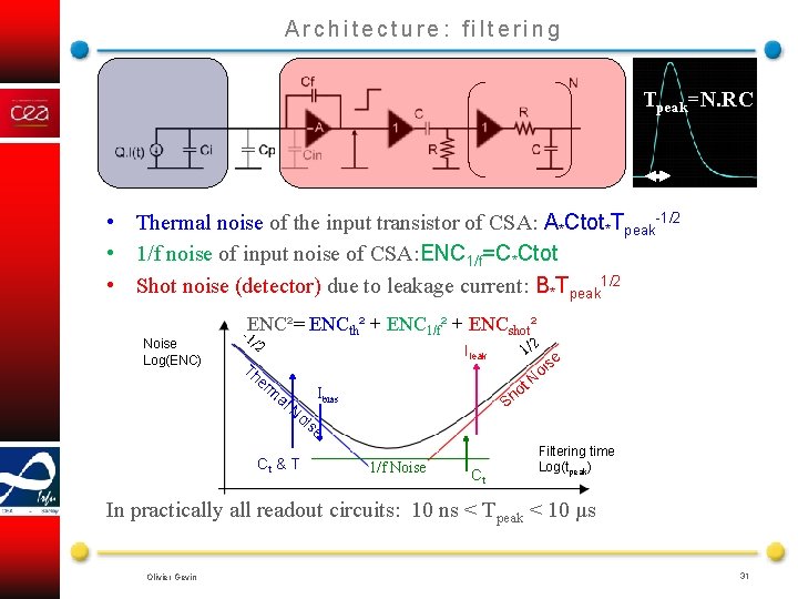
Architecture: filtering Tpeak=N. RC Main noise contributions at the output of the CR-RCN filter : • Thermal noise of the input transistor of CSA • 1/f noise of input noise of CSA (in 1/f) • Shot noise due to leakage current (in 1/f 2) Their relative contributions depend on the peaking time Tpeak=N. RC The peaking time is an optimization parameter and is thus very often programmable. Olivier Gevin 30

Architecture: filtering Tpeak=N. RC • Thermal noise of the input transistor of CSA: A*Ctot*Tpeak-1/2 • 1/f noise of input noise of CSA: ENC 1/f=C*Ctot • Shot noise (detector) due to leakage current: B*Tpeak 1/2 Noise Log(ENC) -1 ENC²= ENCth² + ENC 1/f² + ENCshot² /2 Ileak 1/2 e s Th oi er N m ot Ibias h al S No ise Ct & T 1/f Noise Ct Filtering time Log(tpeak) In practically all readout circuits: 10 ns < Tpeak < 10 µs Olivier Gevin 31

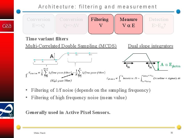
Architecture: filtering and measurement Conversion E=>Q Conversion Q=> V Filtering V Measure V E Detection E>Eth? Time variant filters Multi-Correlated Double Sampling (MCDS) Dual slope integrators tm tm A Ephoton f • Filtering of 1/f noise (depends on the sampling frequency) • Filtering of high frequency noise (mean value) Generally used in Active Pixel Sensors. Olivier Gevin 32

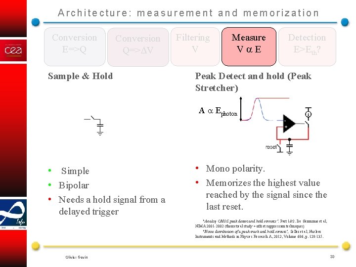
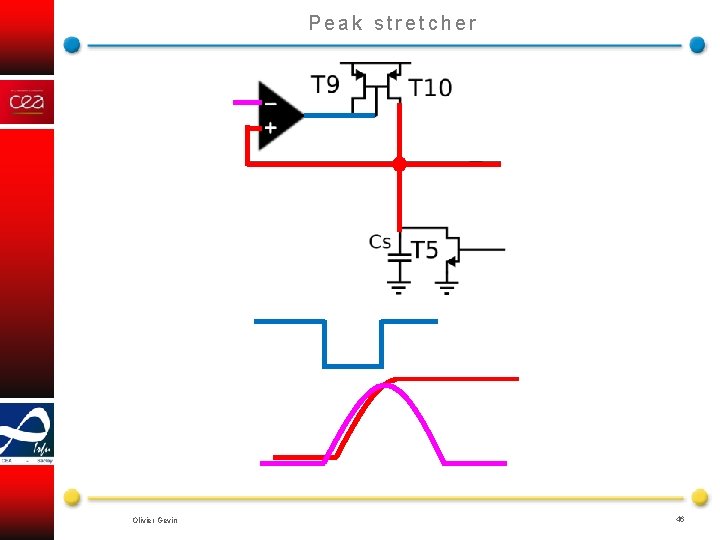
Architecture: measurement and memorization Conversion E=>Q Conversion Q=> V Sample & Hold Filtering V Measure V E Detection E>Eth? Peak Detect and hold (Peak Stretcher) A Ephoton + • Simple • Bipolar • Needs a hold signal from a delayed trigger • Mono polarity. • Memorizes the highest value reached by the signal since the last reset. “Analog CMOS peak detect and hold circuits”. Part 1&2. De Geronimo et al, NIMA 2001 -2002 (theoretical study + offset suppression techniques) “Noise distribution of a peak track and hold circuit”, Seller et al, Nuclear Instruments and Methods in Physics Research A, 2012, Volume 696, p. 129 -135. Olivier Gevin 33

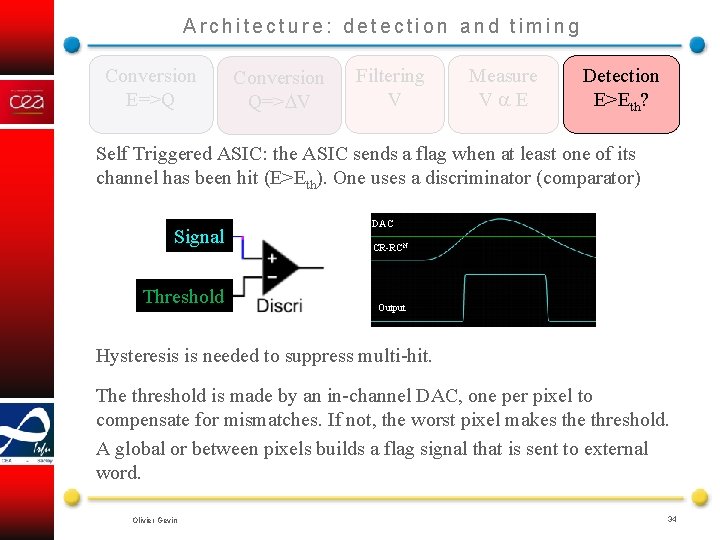
Architecture: detection and timing Conversion E=>Q Conversion Q=> V Filtering V Measure V E Detection E>Eth? Self Triggered ASIC: the ASIC sends a flag when at least one of its channel has been hit (E>Eth). One uses a discriminator (comparator) Signal Threshold DAC CR-RCN Output Hysteresis is needed to suppress multi-hit. The threshold is made by an in-channel DAC, one per pixel to compensate for mismatches. If not, the worst pixel makes the threshold. A global or between pixels builds a flag signal that is sent to external word. Olivier Gevin 34

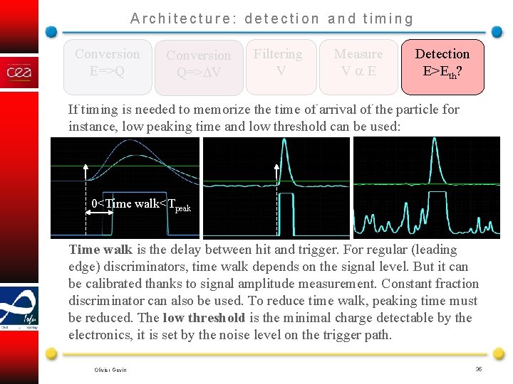
Architecture: detection and timing Conversion E=>Q Conversion Q=> V Filtering V Measure V E Detection E>Eth? If timing is needed to memorize the time of arrival of the particle for instance, low peaking time and low threshold can be used: 0<Time walk<Tpeak Time walk is the delay between hit and trigger. For regular (leading edge) discriminators, time walk depends on the signal level. But it can be calibrated thanks to signal amplitude measurement. Constant fraction discriminator can also be used. To reduce time walk, peaking time must be reduced. The low threshold is the minimal charge detectable by the electronics, it is set by the noise level on the trigger path. Olivier Gevin 35

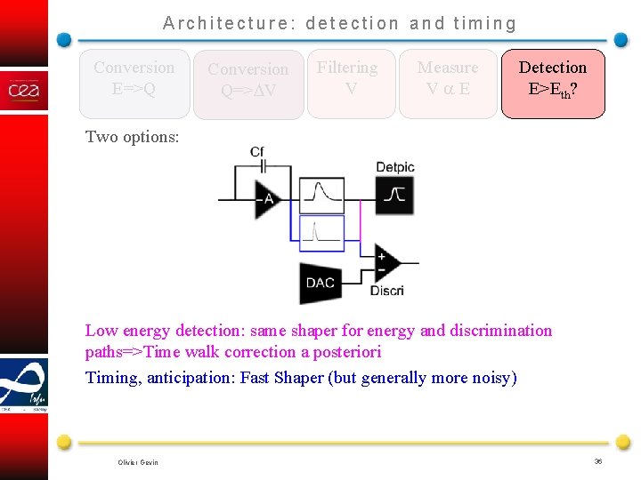
Architecture: detection and timing Conversion E=>Q Conversion Q=> V Filtering V Measure V E Detection E>Eth? Two options: Low energy detection: same shaper for energy and discrimination paths=>Time walk correction a posteriori Timing, anticipation: Fast Shaper (but generally more noisy) Olivier Gevin 36

Erholung Olivier Gevin 37

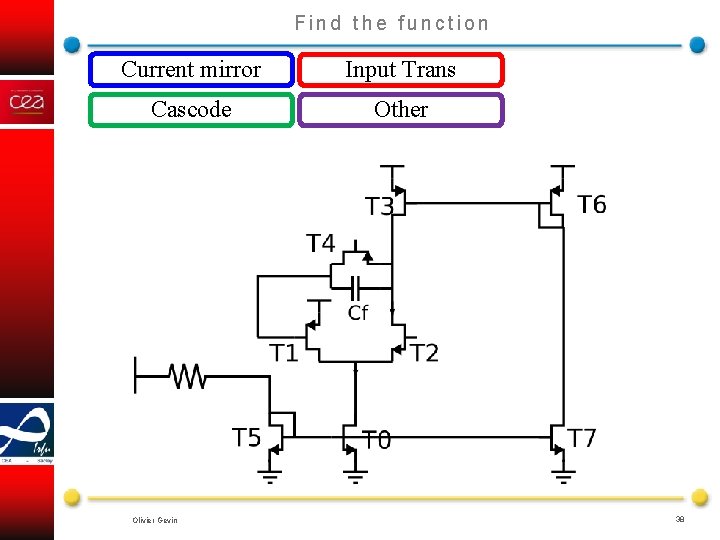
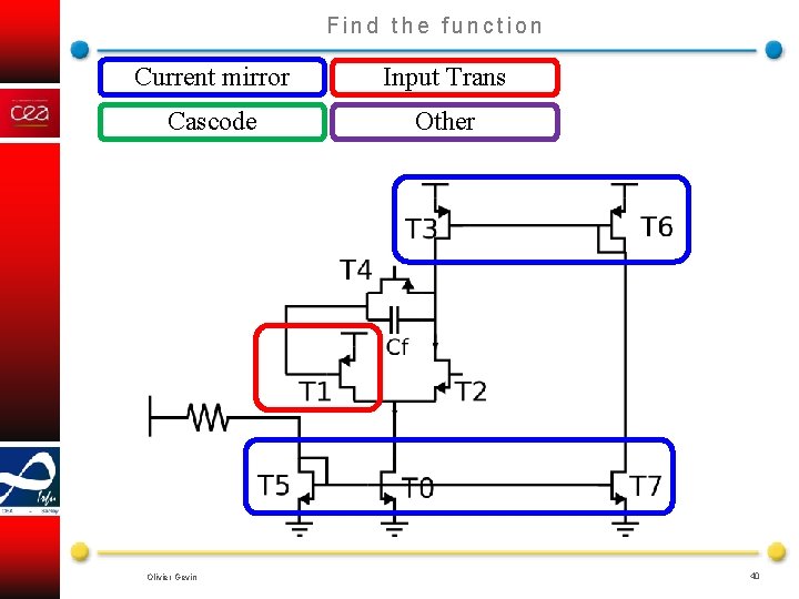
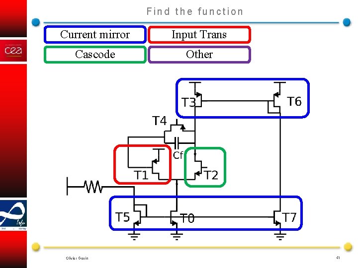
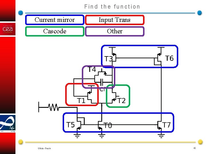
Find the function Current mirror Input Trans Cascode Other Olivier Gevin 38

Find the function Current mirror Input Trans Cascode Other Olivier Gevin 39

Find the function Current mirror Input Trans Cascode Other Olivier Gevin 40

Find the function Current mirror Input Trans Cascode Other Olivier Gevin 41

Find the function Current mirror Input Trans Cascode Other Olivier Gevin 42

Find the function Current mirror Input Trans Cascode Other Folded cascode charge preamplifier Olivier Gevin 43

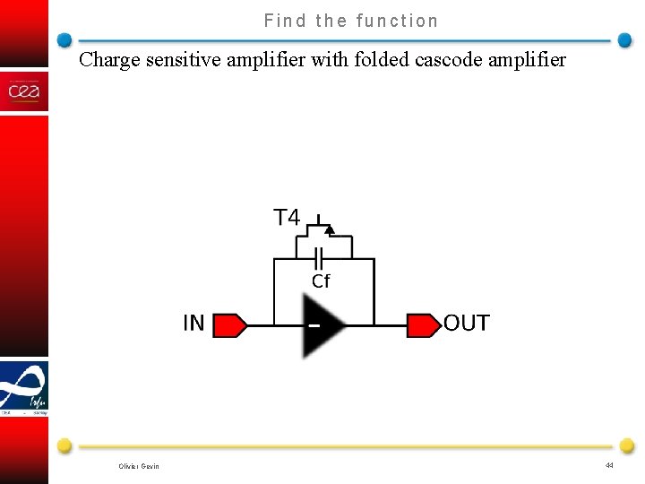
Find the function Charge sensitive amplifier with folded cascode amplifier Olivier Gevin 44

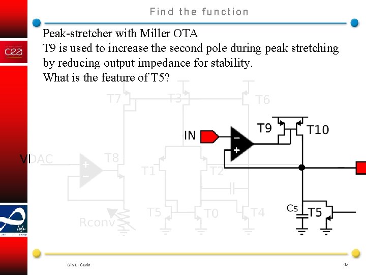
Find the function Peak-stretcher with Miller OTA T 9 is used to increase the second pole during peak stretching by reducing output impedance for stability. What is the feature of T 5? Olivier Gevin 45

Peak stretcher Olivier Gevin 46

Ende Olivier Gevin 47

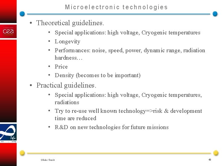
Microelectronic technologies • Theoretical guidelines. • Special applications: high voltage, Cryogenic temperatures • Longevity • Performances: noise, speed, power, dynamic range, radiation hardness… • Price • Density (becomes to be important) • Practical guidelines. • Special applications: high voltage, Cryogenic temperatures, radiations • Try to re-use well known technology=>risk & development time are reduced • R&D on new technologies for future missions Olivier Gevin 48

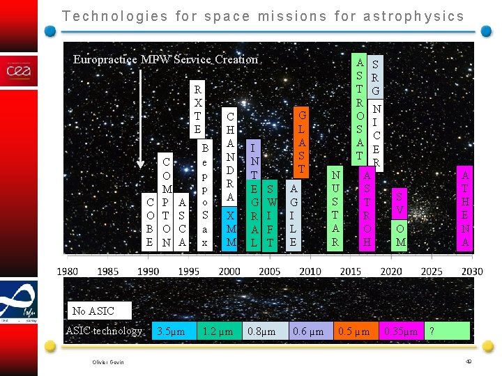
Technologies for space missions for astrophysics Europractice MPW Service Creation R X T E C O B E C O M P T O N A S C A B e p p o S a x C H A N D R A X M M I N T E G R A L G L A S T S W I F T A G I L E A S T R O S A T N U S T A R A S T R O H S R G N I C E R S V O M A T H E N A No ASIC technology: 3. 5µm Olivier Gevin 1. 2 µm 0. 8µm 0. 6 µm 0. 5 µm 0. 35µm ? 49

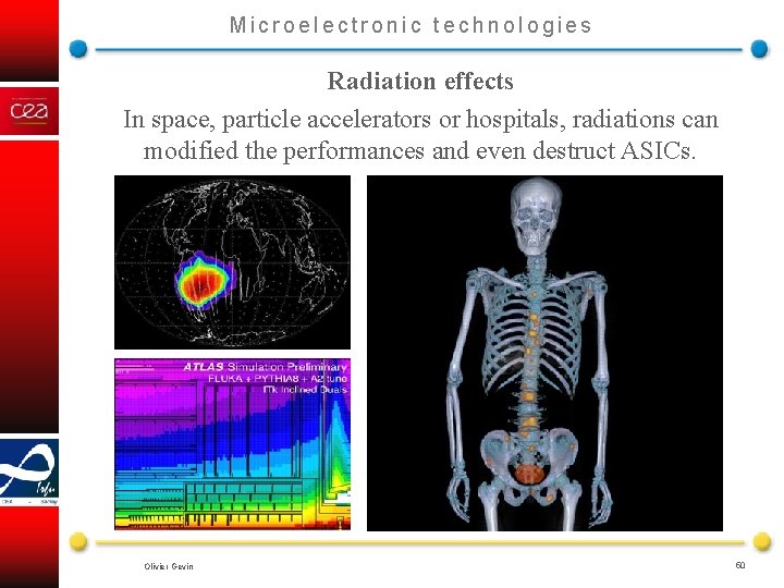
Microelectronic technologies Radiation effects In space, particle accelerators or hospitals, radiations can modified the performances and even destruct ASICs. Olivier Gevin 50

Microelectronic technologies • Dose effects • Radiation-induced charges are trapped in the oxides of the IC=> Vth shifts and carrier mobilities degradation leakge current increase => performances shift (gain, noise, impedance…) and functionality can disappear. . . • Mitigation techniques • Use “aggressive” technologies with thinner oxides (65 nm is the most aggressive today, used for trackers) • Shielding in the instrument (usual in satellites) • Hardening by design: special structures (layout) to mitigate these effects. The received Total Ionizing Dose is typically between few krad and 100 krad (1 k. Gy) for space mission but can reach 1 Grad at LHC in the primary vertex center. Olivier Gevin 51

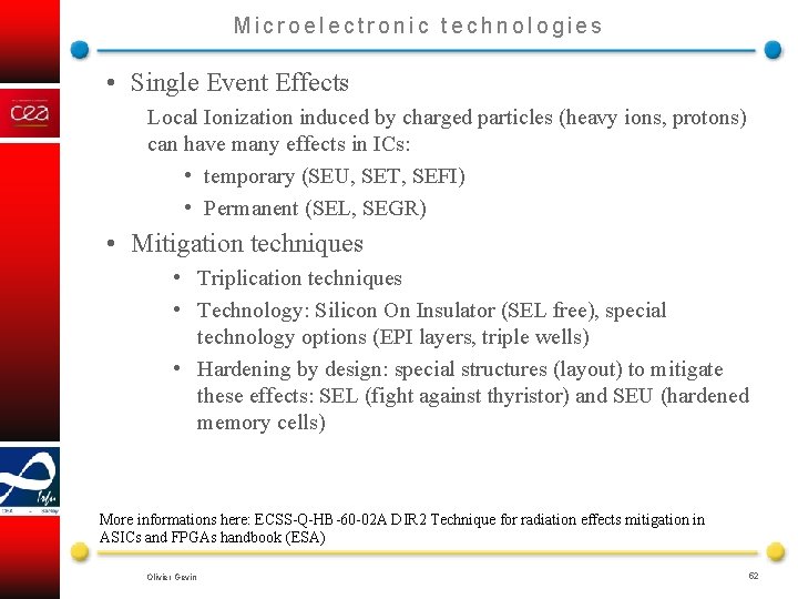
Microelectronic technologies • Single Event Effects Local Ionization induced by charged particles (heavy ions, protons) can have many effects in ICs: • temporary (SEU, SET, SEFI) • Permanent (SEL, SEGR) • Mitigation techniques • Triplication techniques • Technology: Silicon On Insulator (SEL free), special technology options (EPI layers, triple wells) • Hardening by design: special structures (layout) to mitigate these effects: SEL (fight against thyristor) and SEU (hardened memory cells) More informations here: ECSS-Q-HB-60 -02 A DIR 2 Technique for radiation effects mitigation in ASICs and FPGAs handbook (ESA) Olivier Gevin 52

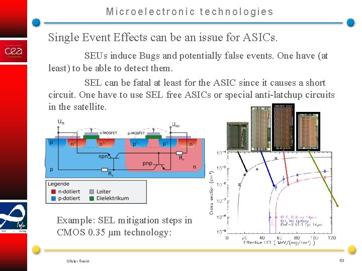
Microelectronic technologies Single Event Effects can be an issue for ASICs. SEUs induce Bugs and potentially false events. One have (at least) to be able to detect them. SEL can be fatal at least for the ASIC since it causes a short circuit. One have to use SEL free ASICs or special anti-latchup circuits in the satellite. Example: SEL mitigation steps in CMOS 0. 35 µm technology: Olivier Gevin 53

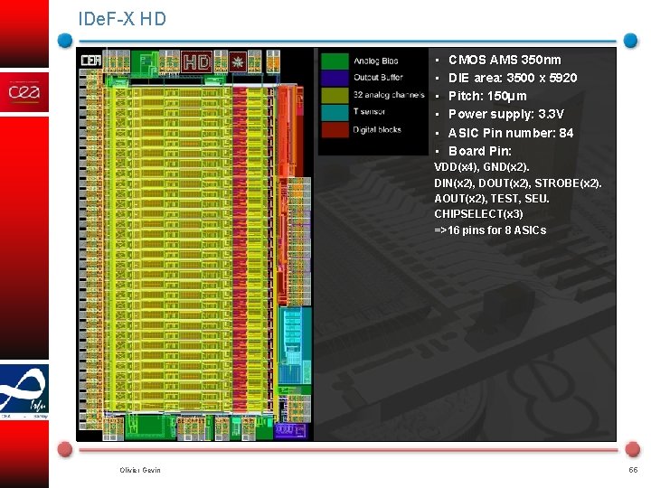
IDe. F-X HD Submitted: december 2009 Come back from fondry: february 2010 Picture of the layout with the different stages, dimensions, ratio between analog and digital part, presentation of the main parts of the layout. Channel, temperature sensor, digital part, buffer…. Olivier Gevin 27 -28 septembre 2016 ASIC analogiques et mixtes pour applications spatiales 54

IDe. F-X HD • CMOS AMS 350 nm Submitted: december 2009 • DIE area: 3500 x 5920 Come back from fondry: february 2010 • Pitch: 150µm Picture of the layout with the different stages, dimensions, ratio between analog and • Power supply: 3. 3 V digital part, presentation of the main parts of the layout. • ASIC Pin number: 84 Channel, temperature sensor, digital part, buffer…. • Board Pin: VDD(x 4), GND(x 2). DIN(x 2), DOUT(x 2), STROBE(x 2). AOUT(x 2), TEST, SEU. CHIPSELECT(x 3) =>16 pins for 8 ASICs Olivier Gevin 55

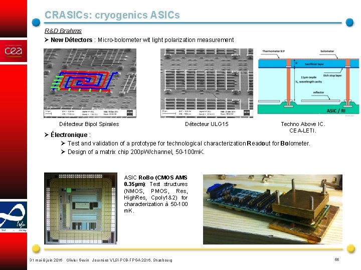
CRASICs: cryogenics ASICs R&D Brahms Ø New Détectors : Micro-bolometer wit light polarization measurement Détecteur ULG 15 Détecteur Bipol Spirales Techno Above IC. CEA-LETI. Ø Électronique : Ø Test and validation of a prototype for technological characterization Readout for Bolometer. Ø Design of a matrix chip 200 p. W/channel, 50 -100 m. K. ASIC Ro. Bo (CMOS AMS 0. 35µm): Test structures (NMOS, PMOS, Res, High. Res, Cpoly 1&2) for characterization à 50 -100 m. K. 31 mai-8 juin 2016 Olivier Gevin Journées VLSI-PCB-FPGA 2016, Strasbourg 56

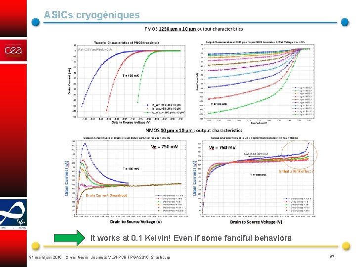
ASICs cryogéniques It works at 0. 1 Kelvin! Even if some fanciful behaviors 31 mai-8 juin 2016 Olivier Gevin Journées VLSI-PCB-FPGA 2016, Strasbourg 57

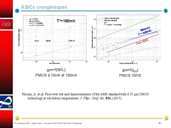
ASICs cryogéniques T°=100 m. K ure Mes K m 100 T°= 300 K Simu gm=f(W/L) PMOS à 10 n. A et 100 n. A gm=f(IDS) PMOS 10/10 Rhouni, A. et al. First-ever test and characterization of the AMS standard bulk 0. 35 μm CMOS technology at sub-kelvin temperatures. J. Phys. Conf. Ser. 834, (2017). 31 mai-8 juin 2016 Olivier Gevin Journées VLSI-PCB-FPGA 2016, Strasbourg 58

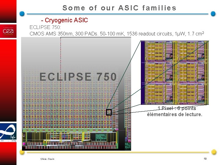
Some of our ASIC families - Cryogenic ASIC ECLIPSE 750: CMOS AMS 350 nm, 300 PADs. 50 -100 m. K, 1536 readout circuits, 1µW, 1. 7 cm 2 ECLIPSE 750 1 Pixel : 6 points élémentaires de lecture. Olivier Gevin 59

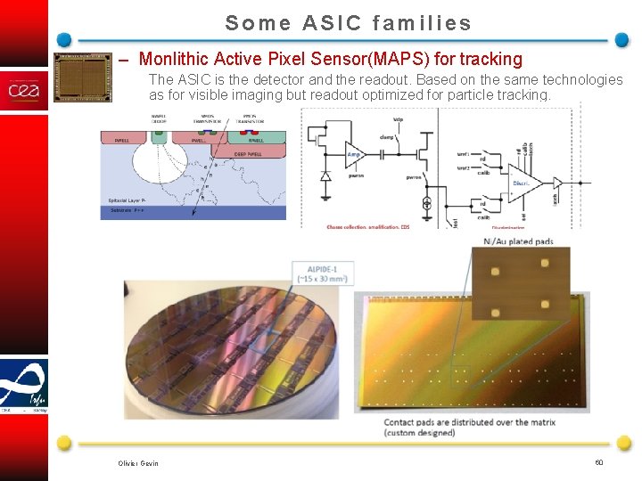
Some ASIC families – Monlithic Active Pixel Sensor(MAPS) for tracking The ASIC is the detector and the readout. Based on the same technologies as for visible imaging but readout optimized for particle tracking. Olivier Gevin 60

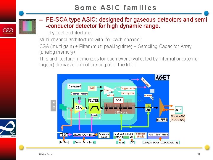
Some ASIC families – FE-SCA type ASIC: designed for gaseous detectors and semi -conductor detector for high dynamic range. Typical architecture Multi-channel architecture with, for each channel: CSA (multi-gain) + Filter (multi peaking time) + Sampling Capacitor Array (analog memory) This architecture memorizes for each event (validated by internal or external trigger) the waveform of the output of the filter: Σ AGET 64 DAC FILTER x 64 in Hit register inhibit SCAwrite SCA CSA TEST SLOW CONTROL In Test Serial Interface ADC x 68 512 cells tpeak Olivier Gevin Trigger pulse Discri Charge range ri. sc di 1 channel 12 -bit ADC BUFFER [ADS 6422] Power on Reset SCA MANAGER Readout W / R Mode CK CK Mode Asic “Spy” Mode CSA; CR; SCAin; DISCRIin(N° 1) 61

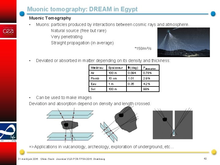
Muonic tomography: DREAM in Egypt Muonic Tomography • Muons: particles produced by interactions between cosmic rays and atmosphere. Natural source (free but rare) Very penetrating Straight propagation (in average) *150/m 2/s • Deviated or absorbed in matter depending on its density and thickness: Matériau Epaisseur (deg) Pabsorption Air 100 m 0. 094 0. 78% Plomb 10 cm 1. 01 2. 9% Eau 1 m 0. 35 4. 2% Sol 100 m 99% • Can be used to make images Deviation and absorption depend on density and length crossed. =>Applications in vulcanology, archeology, exploration of underground, etc… 31 mai-8 juin 2016 Olivier Gevin Journées VLSI-PCB-FPGA 2016, Strasbourg 62

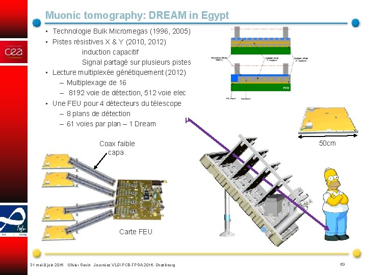
Muonic tomography: DREAM in Egypt • Technologie Bulk Micromegas (1996, 2005) • Pistes résistives X & Y (2010, 2012) induction capacitif Signal partagé sur plusieurs pistes • Lecture multiplexée génétiquement (2012) – Multiplexage de 16 – 8192 voie de détection, 512 voie elec • Une FEU pour 4 détecteurs du télescope – 8 plans de détection µ – 61 voies par plan – 1 Dream Coax faible capa. 50 cm Carte FEU 31 mai-8 juin 2016 Olivier Gevin Journées VLSI-PCB-FPGA 2016, Strasbourg 63

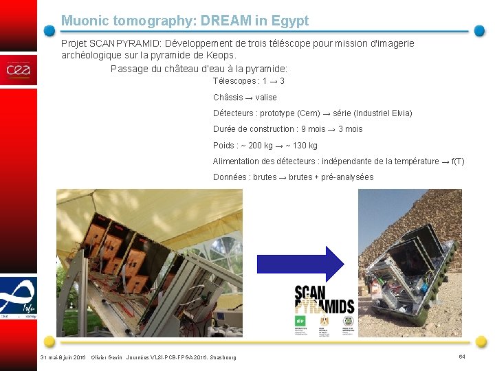
Muonic tomography: DREAM in Egypt Projet SCANPYRAMID: Développement de trois téléscope pour mission d'imagerie archéologique sur la pyramide de Keops. Passage du château d’eau à la pyramide: Télescopes : 1 → 3 Châssis → valise Détecteurs : prototype (Cern) → série (Industriel Elvia) Durée de construction : 9 mois → 3 mois Poids : ~ 200 kg → ~ 130 kg Alimentation des détecteurs : indépendante de la température → f(T) Données : brutes → brutes + pré-analysées 31 mai-8 juin 2016 Olivier Gevin Journées VLSI-PCB-FPGA 2016, Strasbourg 64

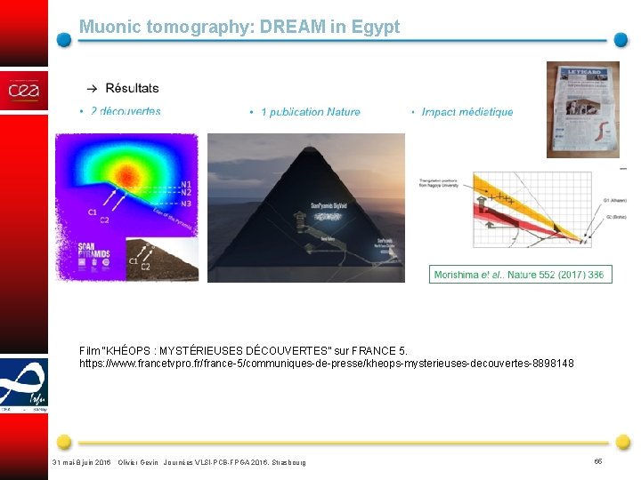
Muonic tomography: DREAM in Egypt Film “KHÉOPS : MYSTÉRIEUSES DÉCOUVERTES” sur FRANCE 5. https: //www. francetvpro. fr/france-5/communiques-de-presse/kheops-mysterieuses-decouvertes-8898148 31 mai-8 juin 2016 Olivier Gevin Journées VLSI-PCB-FPGA 2016, Strasbourg 65

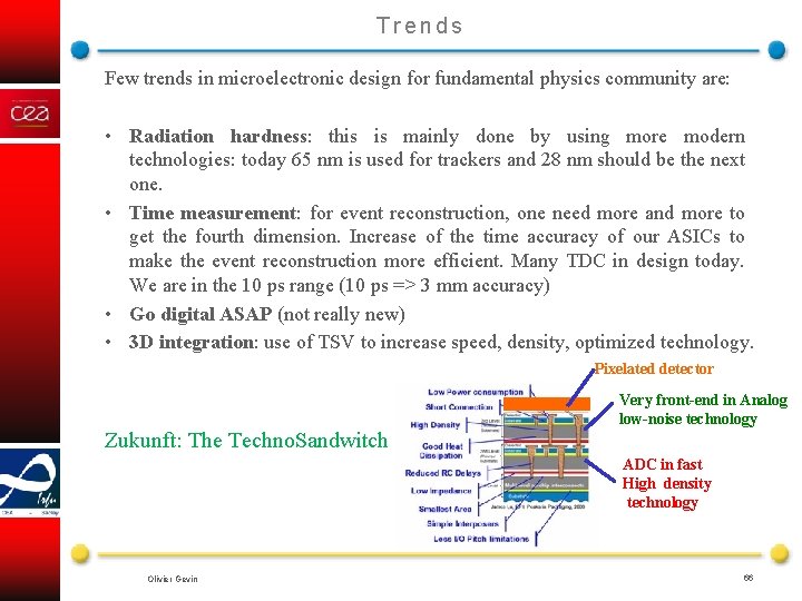
Trends Few trends in microelectronic design for fundamental physics community are: • Radiation hardness: this is mainly done by using more modern technologies: today 65 nm is used for trackers and 28 nm should be the next one. • Time measurement: for event reconstruction, one need more and more to get the fourth dimension. Increase of the time accuracy of our ASICs to make the event reconstruction more efficient. Many TDC in design today. We are in the 10 ps range (10 ps => 3 mm accuracy) • Go digital ASAP (not really new) • 3 D integration: use of TSV to increase speed, density, optimized technology. Pixelated detector Very front-end in Analog low-noise technology Zukunft: The Techno. Sandwitch ADC in fast High density technology Olivier Gevin 66