Forschungszentrum Jlich in der HelmholtzGemeinschaft RF Power improvement

- Slides: 58

Forschungszentrum Jülich in der Helmholtz-Gemeinschaft RF Power improvement of Al. Ga. N/Ga. N based HFETs and MOSHFETs A. Fox, M. Marso B. CWRF 2008 CERN CWRF 2008

Research Center Juelich? Forschungszentrum Jülich in der Helmholtz-Gemeinschaft Where: » between Cologne>>>>>Aachen areas of research : » M aterial » E nvironment » I nformation » L ife » E nergie » Established more than 50 years CWRF 2008 2

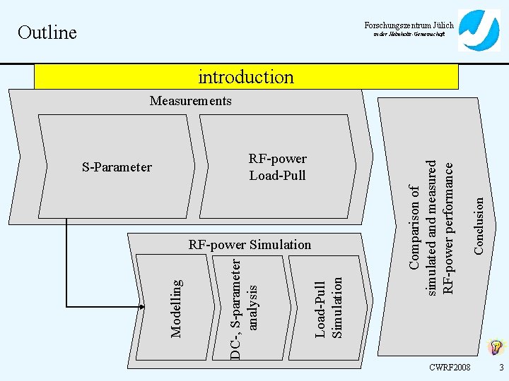
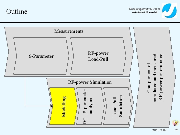
Forschungszentrum Jülich Outline in der Helmholtz-Gemeinschaft introduction Load-Pull Simulation DC-, S-parameter analysis Modelling RF-power Simulation CWRF 2008 Conclusion RF-power Load-Pull S-Parameter Comparison of simulated and measured RF-power performance Measurements 3

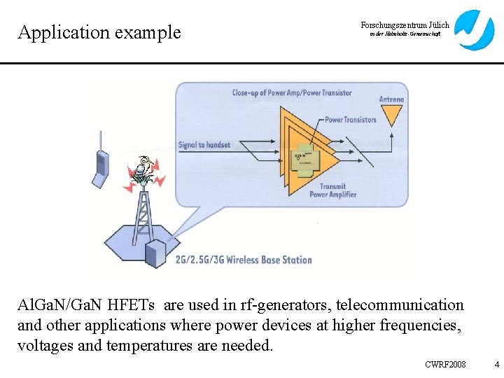
Application example Forschungszentrum Jülich in der Helmholtz-Gemeinschaft Al. Ga. N/Ga. N HFETs are used in rf-generators, telecommunication and other applications where power devices at higher frequencies, voltages and temperatures are needed. CWRF 2008 4

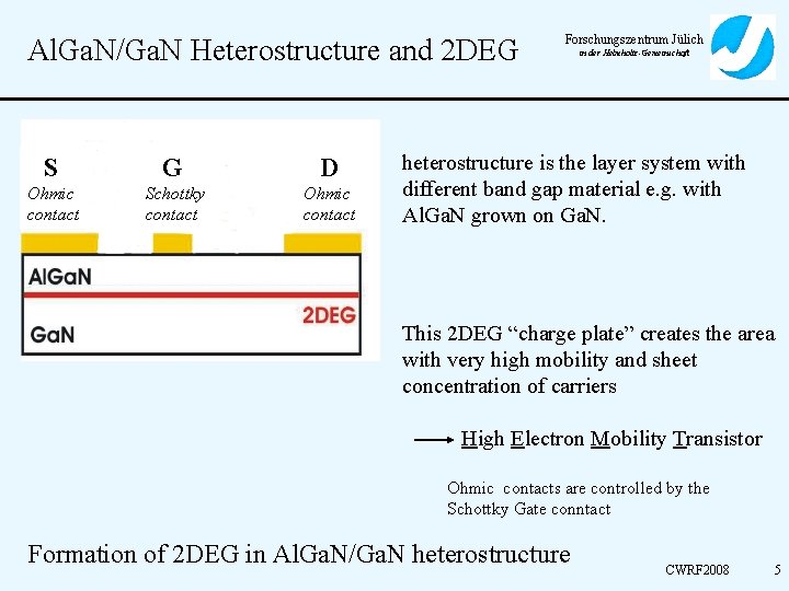
Al. Ga. N/Ga. N Heterostructure and 2 DEG S G D Ohmic contact Schottky contact Ohmic contact Forschungszentrum Jülich in der Helmholtz-Gemeinschaft heterostructure is the layer system with different band gap material e. g. with Al. Ga. N grown on Ga. N. This 2 DEG “charge plate” creates the area with very high mobility and sheet concentration of carriers High Electron Mobility Transistor Ohmic contacts are controlled by the Schottky Gate conntact Formation of 2 DEG in Al. Ga. N/Ga. N heterostructure CWRF 2008 5

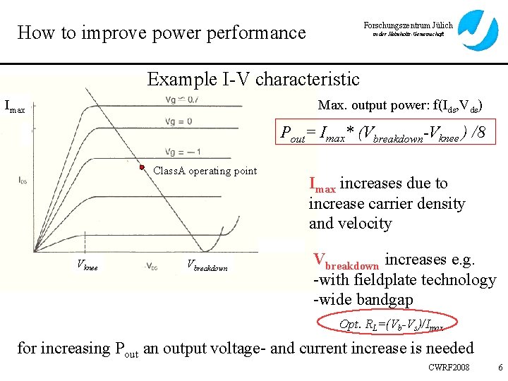
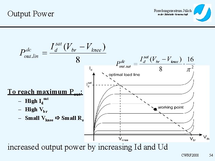
Forschungszentrum Jülich How to improve power performance in der Helmholtz-Gemeinschaft Example I-V characteristic Imax Max. output power: f(Ids, Vds) Pout= Imax* (Vbreakdown-Vknee ) /8 Class. A operating point Vknee Vbreakdown Imax increases due to increase carrier density and velocity Vbreakdown increases e. g. -with fieldplate technology -wide bandgap Opt. RL=(Vb-Vs)/Imax for increasing Pout an output voltage- and current increase is needed CWRF 2008 6

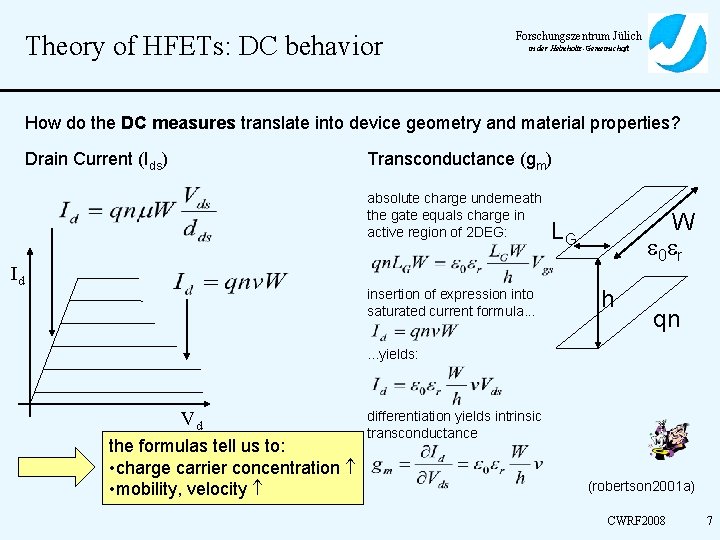
Theory of HFETs: DC behavior Forschungszentrum Jülich in der Helmholtz-Gemeinschaft How do the DC measures translate into device geometry and material properties? Drain Current (Ids) Transconductance (gm) absolute charge underneath the gate equals charge in active region of 2 DEG: Id insertion of expression into saturated current formula. . . W 0 r LG h qn . . . yields: Vd the formulas tell us to: • charge carrier concentration • mobility, velocity differentiation yields intrinsic transconductance (robertson 2001 a) CWRF 2008 7

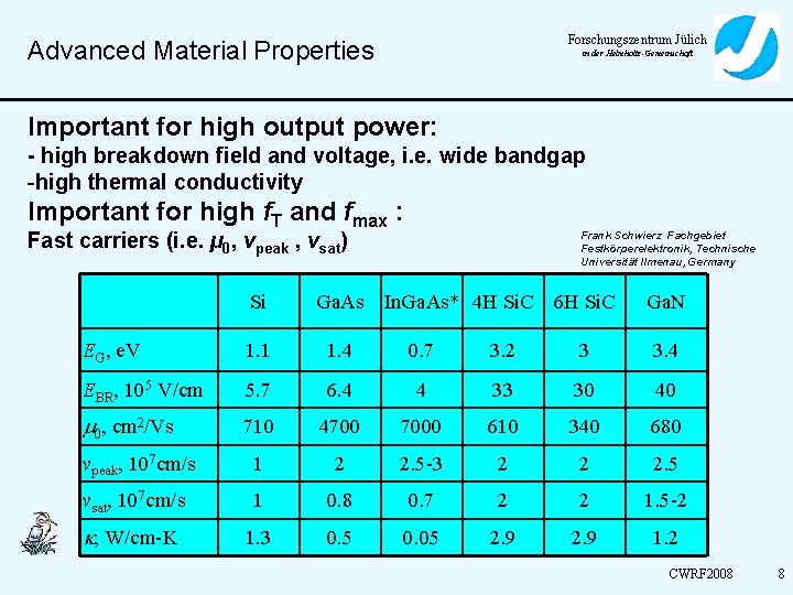
Forschungszentrum Jülich Advanced Material Properties in der Helmholtz-Gemeinschaft Important for high output power: - high breakdown field and voltage, i. e. wide bandgap -high thermal conductivity Important for high f. T and fmax : Fast carriers (i. e. µ 0, vpeak , vsat) Si Frank Schwierz Fachgebiet Festkörperelektronik, Technische Universität Ilmenau, Germany Ga. As In. Ga. As* 4 H Si. C 6 H Si. C Ga. N EG, e. V 1. 1 1. 4 0. 7 3. 2 3 3. 4 EBR, 105 V/cm 5. 7 6. 4 4 33 30 40 m 0, cm 2/Vs 710 4700 7000 610 340 680 vpeak, 107 cm/s 1 2 2. 5 -3 2 2 2. 5 vsat, 107 cm/s 1 0. 8 0. 7 2 2 1. 5 -2 k, W/cm-K 1. 3 0. 5 0. 05 2. 9 1. 2 CWRF 2008 8

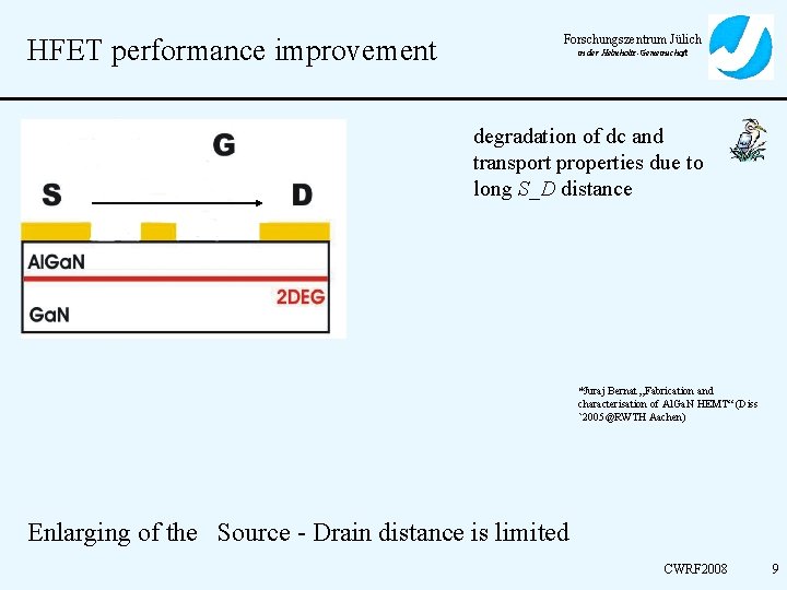
HFET performance improvement Forschungszentrum Jülich in der Helmholtz-Gemeinschaft degradation of dc and transport properties due to long S_D distance *Juraj Bernat „Fabrication and characterisation of Al. Ga. N HEMT“ (Diss `2005@RWTH Aachen) Enlarging of the Source - Drain distance is limited CWRF 2008 9

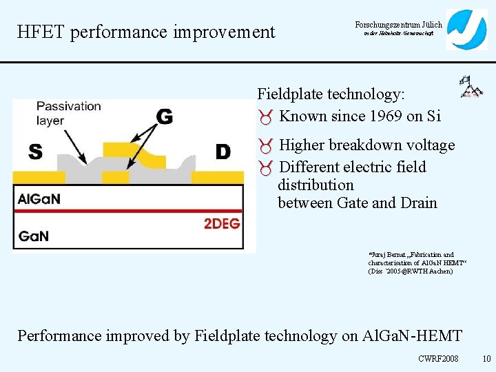
HFET performance improvement Forschungszentrum Jülich in der Helmholtz-Gemeinschaft Fieldplate technology: Known since 1969 on Si Higher breakdown voltage Different electric field distribution between Gate and Drain *Juraj Bernat „Fabrication and characterisation of Al. Ga. N HEMT“ (Diss `2005@RWTH Aachen) Performance improved by Fieldplate technology on Al. Ga. N-HEMT CWRF 2008 10

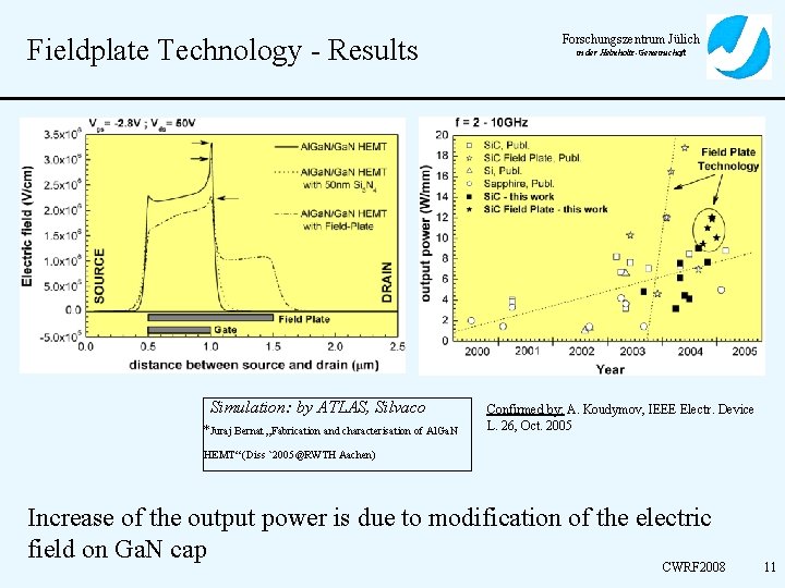
Fieldplate Technology - Results Simulation: by ATLAS, Silvaco *Juraj Bernat „Fabrication and characterisation of Al. Ga. N Forschungszentrum Jülich in der Helmholtz-Gemeinschaft Confirmed by: A. Koudymov, IEEE Electr. Device L. 26, Oct. 2005 HEMT“ (Diss `2005@RWTH Aachen) Increase of the output power is due to modification of the electric field on Ga. N cap CWRF 2008 11

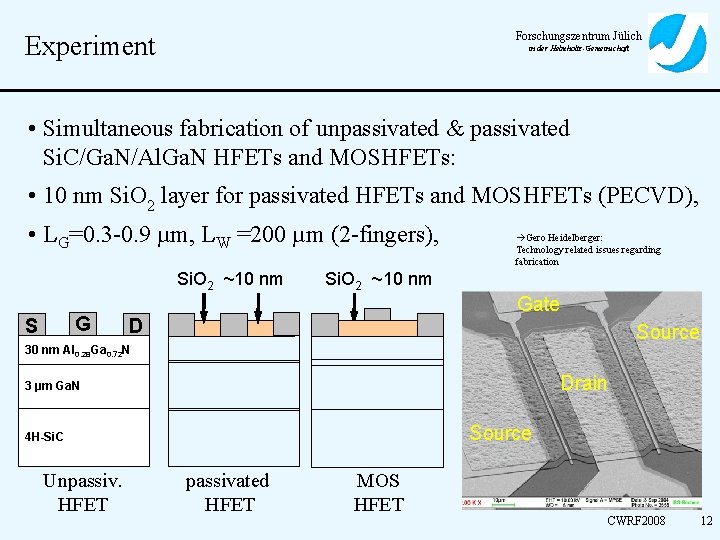
Forschungszentrum Jülich Experiment in der Helmholtz-Gemeinschaft • Simultaneous fabrication of unpassivated & passivated Si. C/Ga. N/Al. Ga. N HFETs and MOSHFETs: • 10 nm Si. O 2 layer for passivated HFETs and MOSHFETs (PECVD), • LG=0. 3 -0. 9 µm, LW =200 µm (2 -fingers), Si. O 2 ~10 nm G S Gero Heidelberger: Technology related issues regarding fabrication Si. O 2 ~10 nm Gate D Source 30 nm Al 0. 28 Ga 0. 72 N Drain 3 µm Ga. N Source 4 H-Si. C Unpassiv. HFET passivated HFET MOS HFET CWRF 2008 12

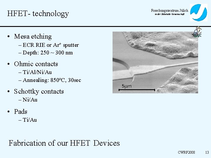
HFET- technology Forschungszentrum Jülich in der Helmholtz-Gemeinschaft • Mesa etching – ECR RIE or Ar+ sputter – Depth: 250 ~ 300 nm • Ohmic contacts – Ti/Al/Ni/Au – Annealing: 850ºC, 30 sec • Schottky contacts – Ni/Au • Pads – Ti/Au Fabrication of our HFET Devices CWRF 2008 13

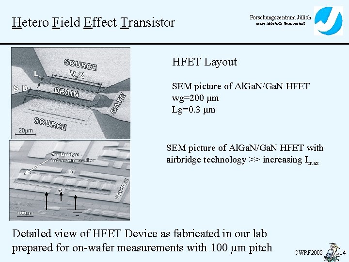
Hetero Field Effect Transistor Forschungszentrum Jülich in der Helmholtz-Gemeinschaft HFET Layout SEM picture of Al. Ga. N/Ga. N HFET wg=200 µm Lg=0. 3 µm SEM picture of Al. Ga. N/Ga. N HFET with airbridge technology >> increasing Imax Detailed view of HFET Device as fabricated in our lab prepared for on-wafer measurements with 100 µm pitch CWRF 2008 14

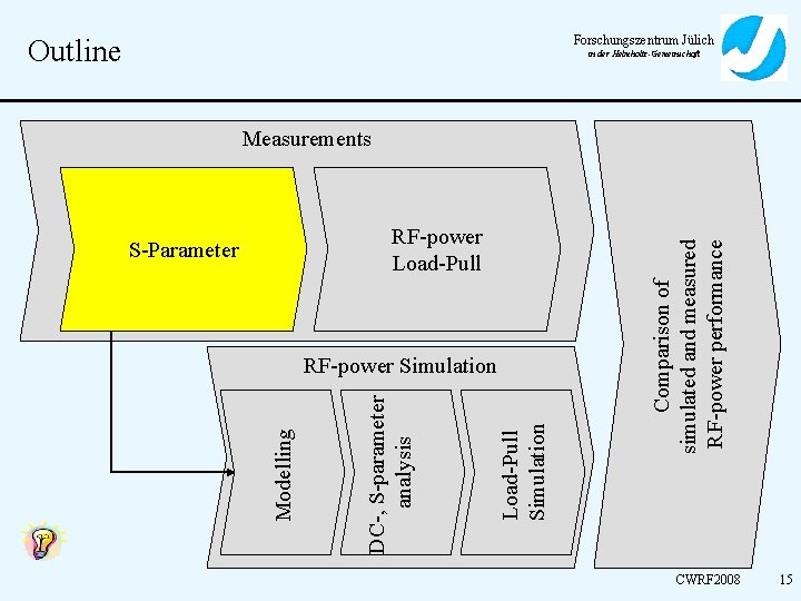
Forschungszentrum Jülich Outline in der Helmholtz-Gemeinschaft RF-power Load-Pull S-Parameter Load-Pull Simulation DC-, S-parameter analysis Modelling RF-power Simulation Comparison of simulated and measured RF-power performance Measurements CWRF 2008 15

S-parameter Measurement System Forschungszentrum Jülich in der Helmholtz-Gemeinschaft • Important for microwave design and characterization • Basics for parameter extraction and simulation • Our measurement system: – Frequency up to 110 GHz – Network Analyzer – On wafer measurements – Control System and Calibration (LRM) CWRF 2008 16

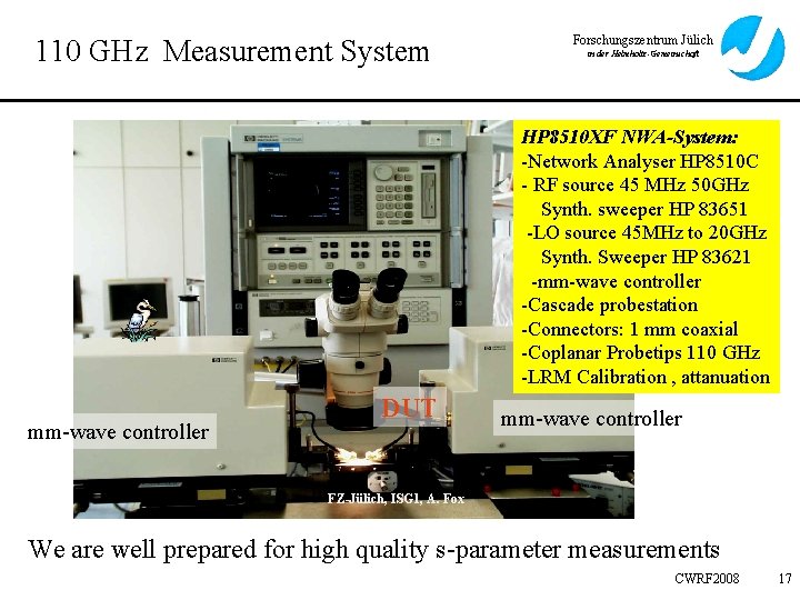
110 GHz Measurement System Forschungszentrum Jülich in der Helmholtz-Gemeinschaft HP 8510 XF NWA-System: -Network Analyser HP 8510 C - RF source 45 MHz 50 GHz Synth. sweeper HP 83651 -LO source 45 MHz to 20 GHz Synth. Sweeper HP 83621 -mm-wave controller -Cascade probestation -Connectors: 1 mm coaxial -Coplanar Probetips 110 GHz -LRM Calibration , attanuation mm-wave controller DUT mm-wave controller FZ-Jülich, ISG 1, A. Fox We are well prepared for high quality s-parameter measurements CWRF 2008 17

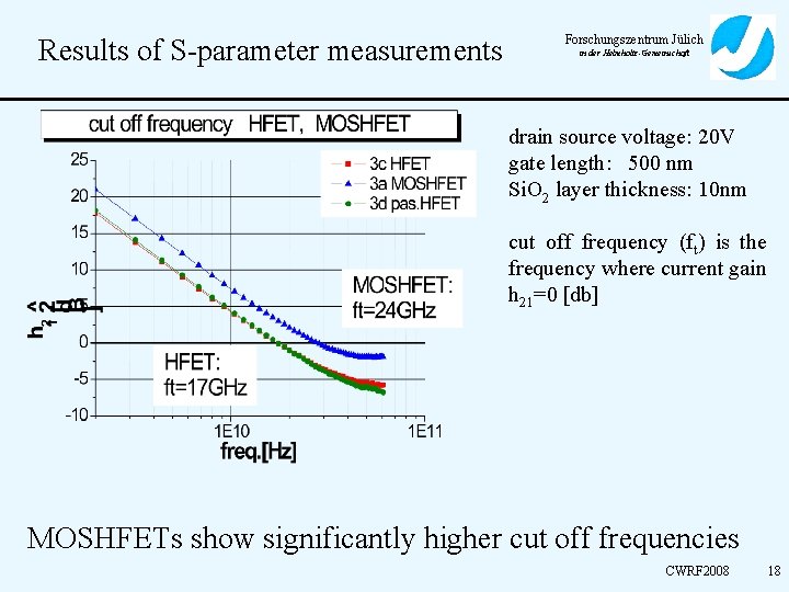
Results of S-parameter measurements Forschungszentrum Jülich in der Helmholtz-Gemeinschaft drain source voltage: 20 V gate length: 500 nm Si. O 2 layer thickness: 10 nm cut off frequency (ft) is the frequency where current gain h 21=0 [db] MOSHFETs show significantly higher cut off frequencies CWRF 2008 18

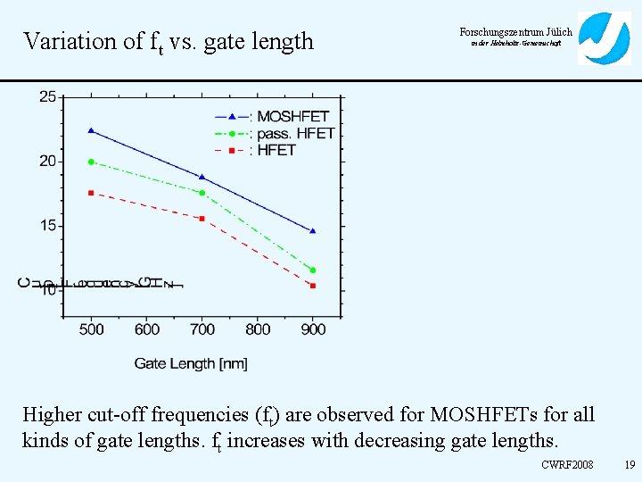
Variation of ft vs. gate length Forschungszentrum Jülich in der Helmholtz-Gemeinschaft Higher cut-off frequencies (ft) are observed for MOSHFETs for all kinds of gate lengths. ft increases with decreasing gate lengths. CWRF 2008 19

Forschungszentrum Jülich Outline in der Helmholtz-Gemeinschaft RF-power Load-Pull S-Parameter Load-Pull Simulation DC-, S-parameter analysis Modelling RF-power Simulation Comparison of simulated and measured RF-power performance Measurements CWRF 2008 20

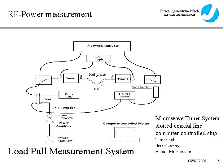
RF-Power measurement Forschungszentrum Jülich in der Helmholtz-Gemeinschaft Ref. plane step attenuator resonanz. Load Pull Measurement System Microwave Tuner System slotted coaxial line computer controlled slug Tuner cal. deembeding Focus Microwave CWRF 2008 21

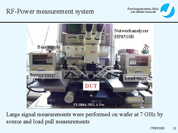
RF-Power measurement system Forschungszentrum Jülich in der Helmholtz-Gemeinschaft Networkanalyzer HP 8510 B Bias supply Source-tuner Load-tuner DUT FZ-Jülich, ISG 1, A. Fox Large signal measurements were performed on wafer at 7 GHz by source and load pull measurements CWRF 2008 22

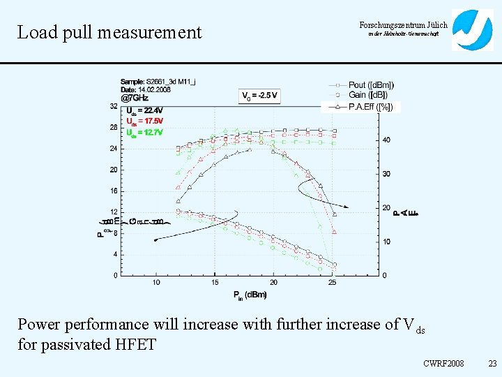
Load pull measurement Forschungszentrum Jülich in der Helmholtz-Gemeinschaft Power performance will increase with further increase of Vds for passivated HFET CWRF 2008 23

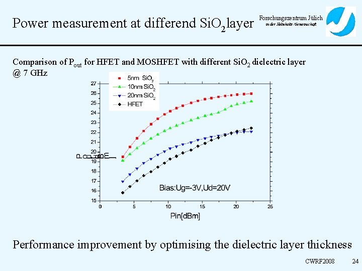
Power measurement at differend Si. O 2 layer Forschungszentrum Jülich in der Helmholtz-Gemeinschaft Comparison of Pout for HFET and MOSHFET with different Si. O 2 dielectric layer @ 7 GHz Performance improvement by optimising the dielectric layer thickness CWRF 2008 24

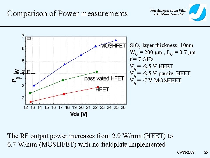
Comparison of Power measurements Forschungszentrum Jülich in der Helmholtz-Gemeinschaft Si. O 2 layer thickness: 10 nm WG = 200 µm , LG = 0. 7 µm f = 7 GHz Vg = -2. 5 V HFET Vg = -2. 5 V passiv. HFET Vg = -7 V MOSHFET The RF output power increases from 2. 9 W/mm (HFET) to 6. 7 W/mm (MOSHFET) with no fieldplate implemented CWRF 2008 25

Forschungszentrum Jülich Outline in der Helmholtz-Gemeinschaft RF-power Load-Pull S-Parameter Load-Pull Simulation DC-, S-parameter analysis Modelling RF-power Simulation Comparison of simulated and measured RF-power performance Measurements CWRF 2008 26

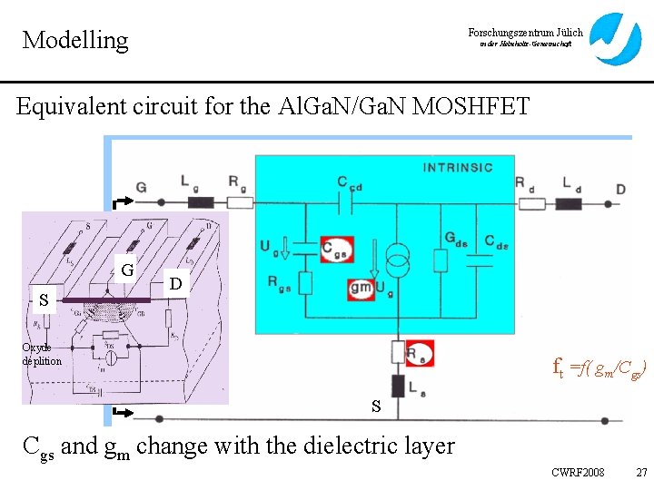
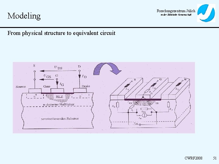
Modelling Forschungszentrum Jülich in der Helmholtz-Gemeinschaft Equivalent circuit for the Al. Ga. N/Ga. N MOSHFET G S D Oxyde deplition ft =f( gm/Cgs) S Cgs and gm change with the dielectric layer CWRF 2008 27

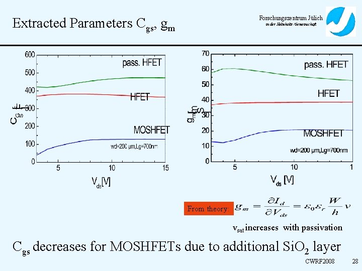
Forschungszentrum Jülich Extracted Parameters Cgs, gm in der Helmholtz-Gemeinschaft From theory: vsat increases with passivation Cgs decreases for MOSHFETs due to additional Si. O 2 layer CWRF 2008 28

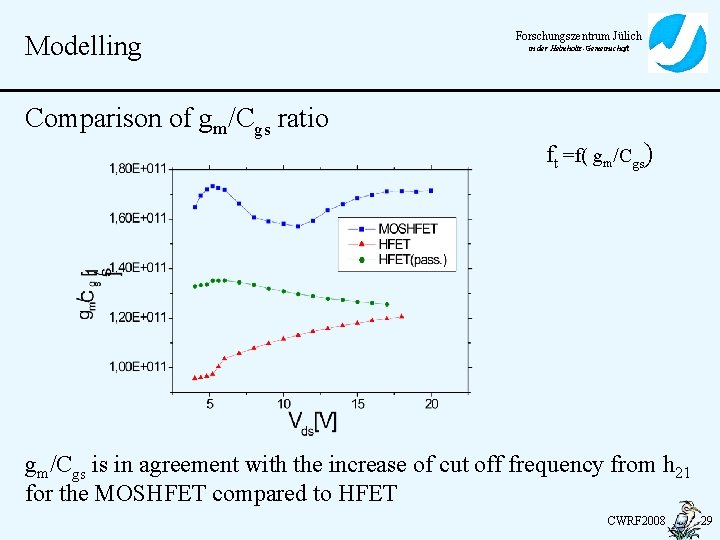
Modelling Comparison of gm/Cgs ratio Forschungszentrum Jülich in der Helmholtz-Gemeinschaft ft =f( gm/Cgs) gm/Cgs is in agreement with the increase of cut off frequency from h 21 for the MOSHFET compared to HFET CWRF 2008 29

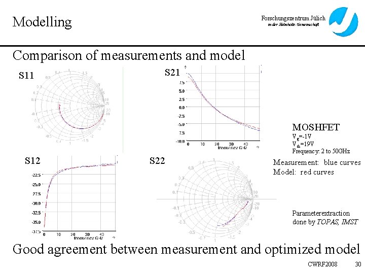
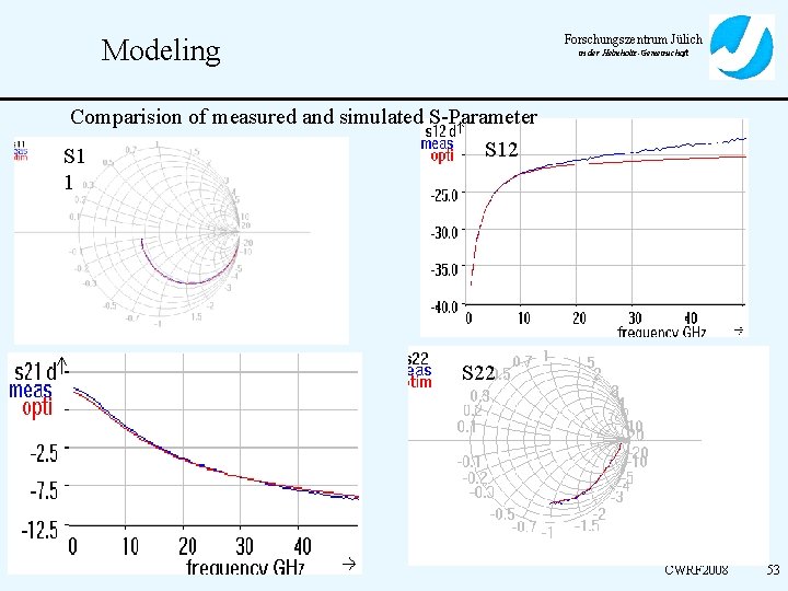
Modelling Forschungszentrum Jülich in der Helmholtz-Gemeinschaft Comparison of measurements and model S 11 S 21 MOSHFET Vg=-1 V Vds=19 V Frequency: 2 to 50 GHz S 12 S 22 Measurement: blue curves Model: red curves Parameterextraction done by TOPAS, IMST Good agreement between measurement and optimized model CWRF 2008 30

Forschungszentrum Jülich Outline in der Helmholtz-Gemeinschaft RF-power Load-Pull S-Parameter Load-Pull Simulation DC-, S-parameter analysis Modelling RF-power Simulation Comparison of simulated and measured RF-power performance Measurements CWRF 2008 31

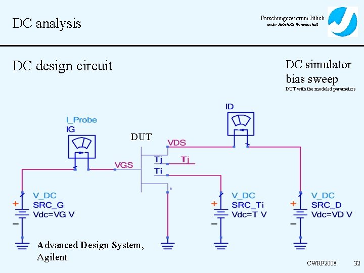
Forschungszentrum Jülich DC analysis in der Helmholtz-Gemeinschaft DC simulator bias sweep DC design circuit DUT with the modeled parameters DUT Advanced Design System, Agilent CWRF 2008 32

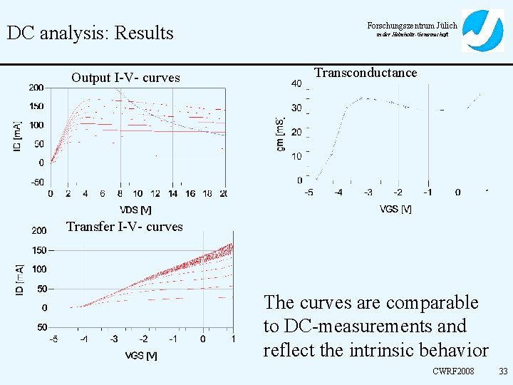
DC analysis: Results Output I-V- curves Forschungszentrum Jülich in der Helmholtz-Gemeinschaft Transconductance Transfer I-V- curves The curves are comparable to DC-measurements and reflect the intrinsic behavior CWRF 2008 33

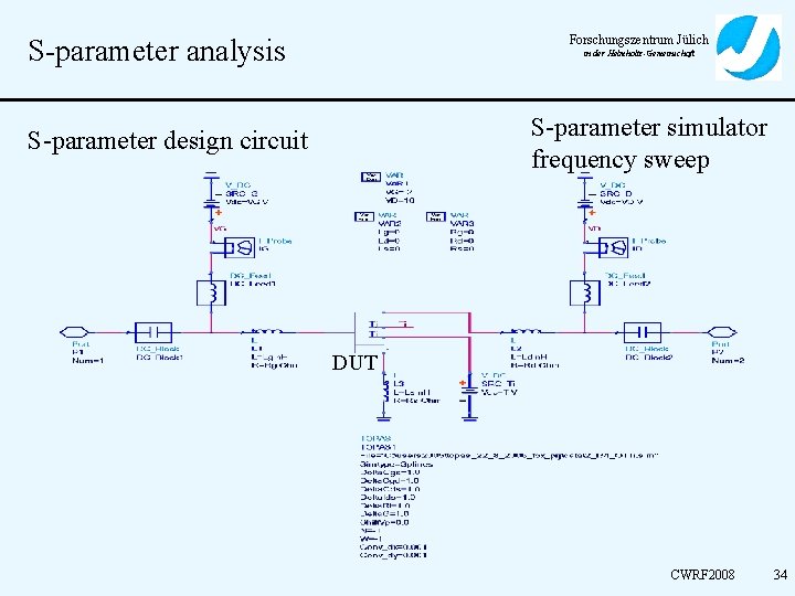
Forschungszentrum Jülich S-parameter analysis in der Helmholtz-Gemeinschaft S-parameter simulator frequency sweep S-parameter design circuit DUT CWRF 2008 34

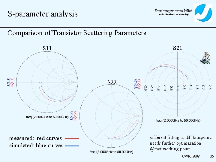
Forschungszentrum Jülich S-parameter analysis in der Helmholtz-Gemeinschaft Comparison of Transistor Scattering Parameters S 21 S 11 S 22 measured: red curves simulated: blue curves different fitting at dif. biaspoints needs further optimazation @that working point CWRF 2008 35

Forschungszentrum Jülich Outline in der Helmholtz-Gemeinschaft RF-power Load-Pull S-Parameter Load-Pull Simulation DC-, S-parameter analysis Modelling RF-power Simulation Comparison of simulated and measured RF-power performance Measurements CWRF 2008 36

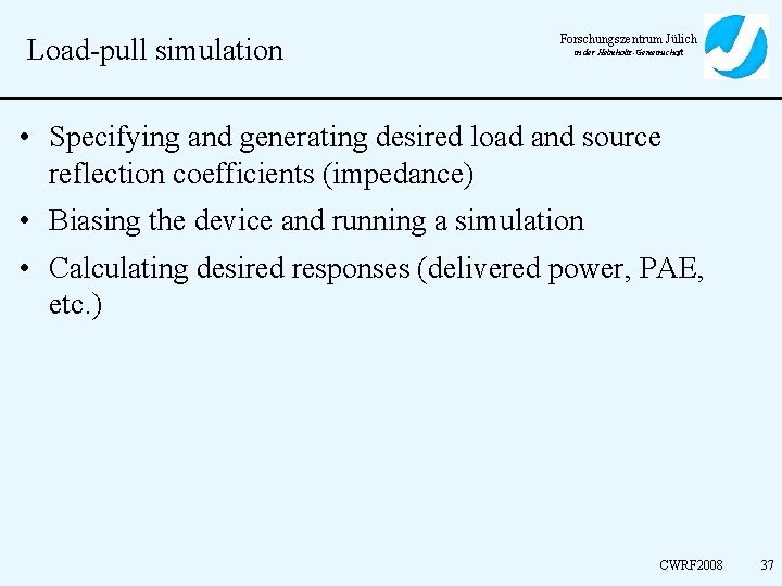
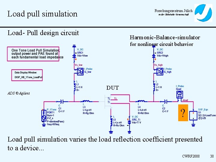
Load-pull simulation Forschungszentrum Jülich in der Helmholtz-Gemeinschaft • Specifying and generating desired load and source reflection coefficients (impedance) • Biasing the device and running a simulation • Calculating desired responses (delivered power, PAE, etc. ) CWRF 2008 37

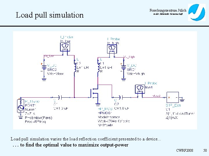
Forschungszentrum Jülich Load pull simulation in der Helmholtz-Gemeinschaft Load- Pull design circuit Harmonic-Balance-simulator for nonlinear circuit behavior DUT ADS © Agilent ? Load pull simulation varies the load reflection coefficient presented to a device. . . CWRF 2008 38

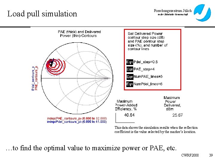
Load pull simulation Forschungszentrum Jülich in der Helmholtz-Gemeinschaft This data shows the simulation results when the reflection coefficient is the value selected by the marker’s location. …to find the optimal value to maximize power or PAE, etc. CWRF 2008 39

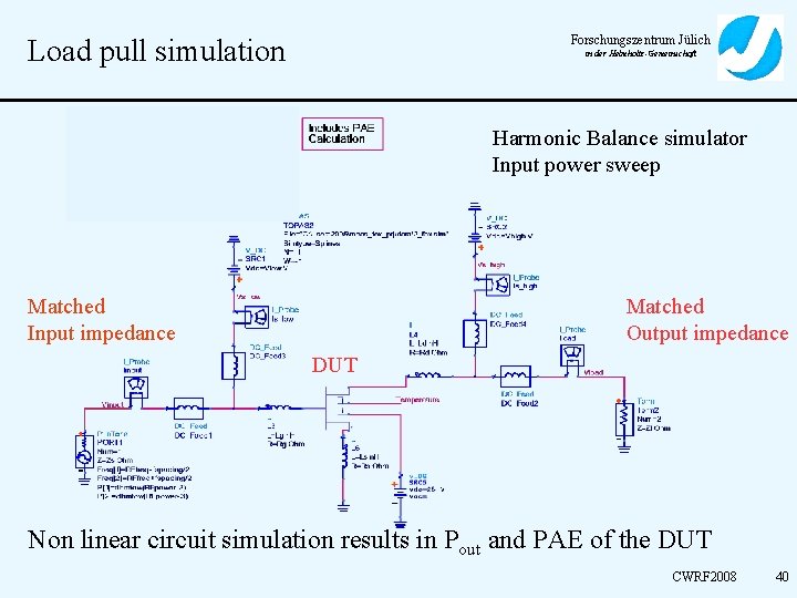
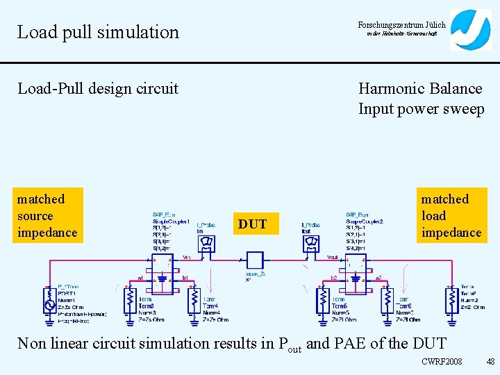
Forschungszentrum Jülich Load pull simulation in der Helmholtz-Gemeinschaft Harmonic Balance simulator Input power sweep Matched Input impedance Matched Output impedance DUT Non linear circuit simulation results in Pout and PAE of the DUT CWRF 2008 40

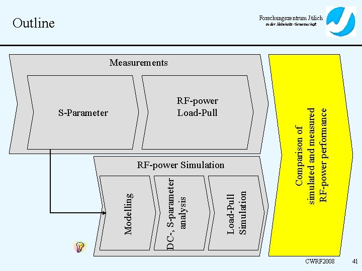
Forschungszentrum Jülich Outline in der Helmholtz-Gemeinschaft RF-power Load-Pull S-Parameter Load-Pull Simulation DC-, S-parameter analysis Modelling RF-power Simulation Comparison of simulated and measured RF-power performance Measurements CWRF 2008 41

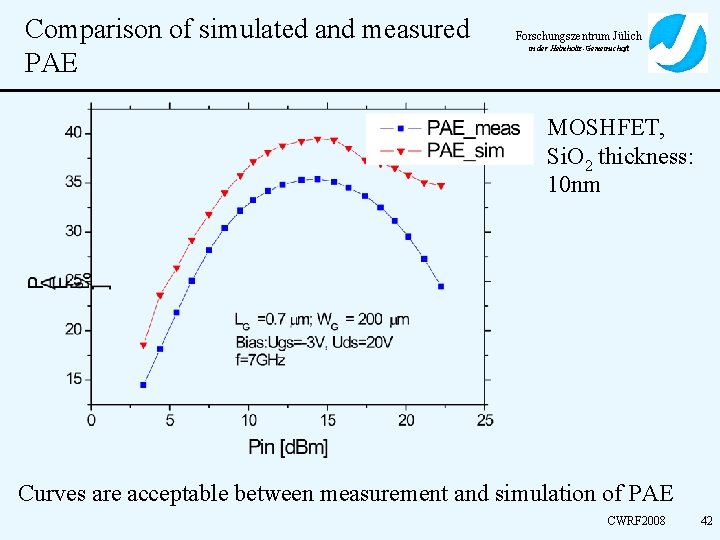
Comparison of simulated and measured PAE Forschungszentrum Jülich in der Helmholtz-Gemeinschaft MOSHFET, Si. O 2 thickness: 10 nm Curves are acceptable between measurement and simulation of PAE CWRF 2008 42

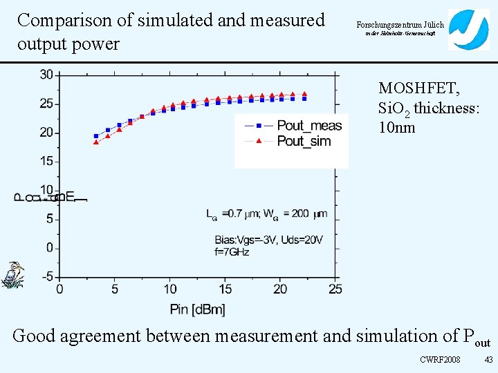
Comparison of simulated and measured output power Forschungszentrum Jülich in der Helmholtz-Gemeinschaft MOSHFET, Si. O 2 thickness: 10 nm Good agreement between measurement and simulation of Pout CWRF 2008 43

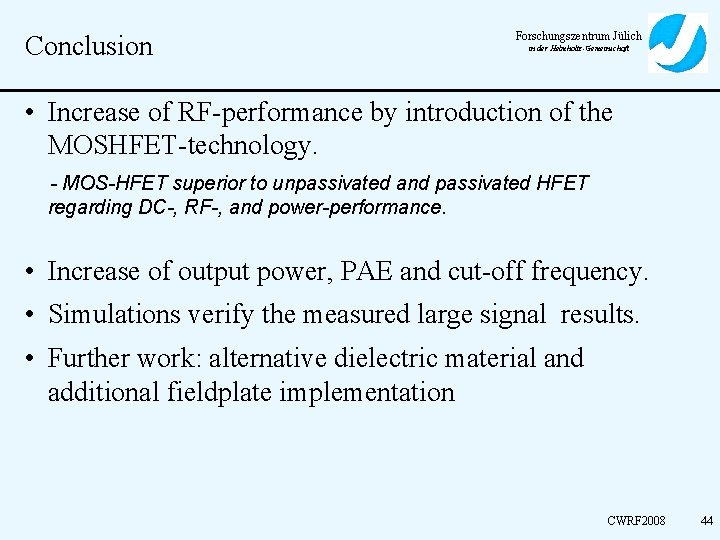
Conclusion Forschungszentrum Jülich in der Helmholtz-Gemeinschaft • Increase of RF-performance by introduction of the MOSHFET-technology. - MOS-HFET superior to unpassivated and passivated HFET regarding DC-, RF-, and power-performance. • Increase of output power, PAE and cut-off frequency. • Simulations verify the measured large signal results. • Further work: alternative dielectric material and additional fieldplate implementation CWRF 2008 44

Forschungszentrum Jülich CWRF 2008 in der Helmholtz-Gemeinschaft Thank you! CWRF 2008 45

ENDE Vortrag Forschungszentrum Jülich in der Helmholtz-Gemeinschaft CWRF 2008 46

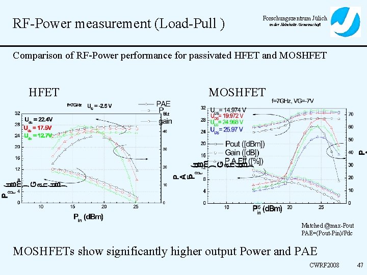
RF-Power measurement (Load-Pull ) Forschungszentrum Jülich in der Helmholtz-Gemeinschaft Comparison of RF-Power performance for passivated HFET and MOSHFET Matched @max-Pout PAE=(Pout-Pin)/Pdc MOSHFETs show significantly higher output Power and PAE CWRF 2008 47

Load pull simulation Forschungszentrum Jülich Load-Pull design circuit Harmonic Balance Input power sweep matched source impedance in der Helmholtz-Gemeinschaft DUT matched load impedance Non linear circuit simulation results in Pout and PAE of the DUT CWRF 2008 48

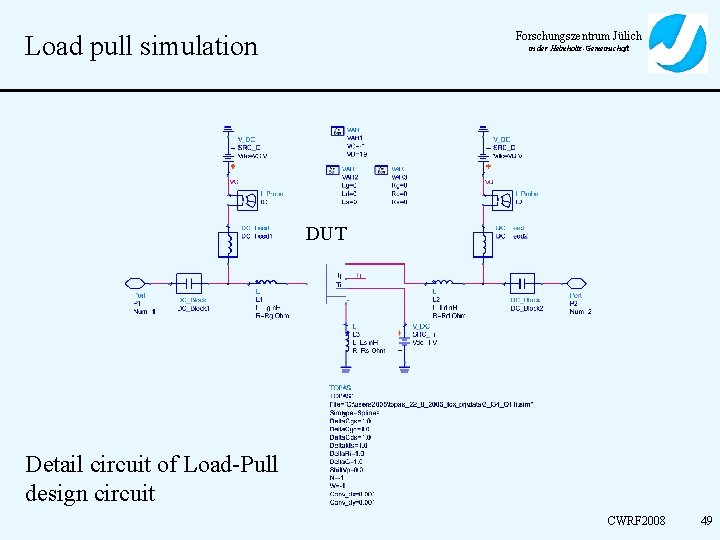
Forschungszentrum Jülich Load pull simulation in der Helmholtz-Gemeinschaft DUT Detail circuit of Load-Pull design circuit CWRF 2008 49

Load pull simulation Forschungszentrum Jülich in der Helmholtz-Gemeinschaft Load pull simulation varies the load reflection coefficient presented to a device. . . …to find the optimal value to maximize output-power CWRF 2008 50

Modeling Forschungszentrum Jülich in der Helmholtz-Gemeinschaft From physical structure to equivalent circuit CWRF 2008 51

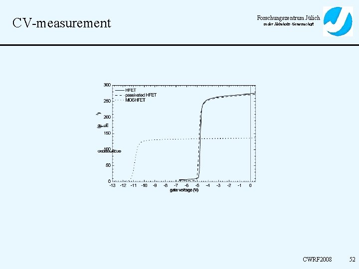
CV-measurement Forschungszentrum Jülich in der Helmholtz-Gemeinschaft CWRF 2008 52

Forschungszentrum Jülich Modeling in der Helmholtz-Gemeinschaft Comparision of measured and simulated S-Parameter S 12 S 1 1 S 22 CWRF 2008 53

Output Power Forschungszentrum Jülich in der Helmholtz-Gemeinschaft To reach maximum Pout: – High Idsat – High Vbr – Small Vknee Small Rs increased output power by increasing Id and Ud CWRF 2008 54

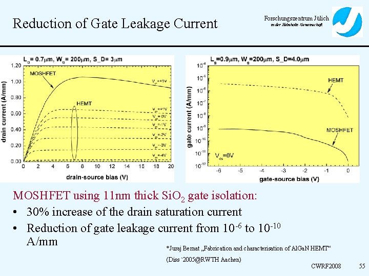
Reduction of Gate Leakage Current Forschungszentrum Jülich in der Helmholtz-Gemeinschaft MOSHFET using 11 nm thick Si. O 2 gate isolation: • 30% increase of the drain saturation current • Reduction of gate leakage current from 10 -6 to 10 -10 A/mm *Juraj Bernat „Fabrication and characterisation of Al. Ga. N HEMT“ (Diss `2005@RWTH Aachen) CWRF 2008 55

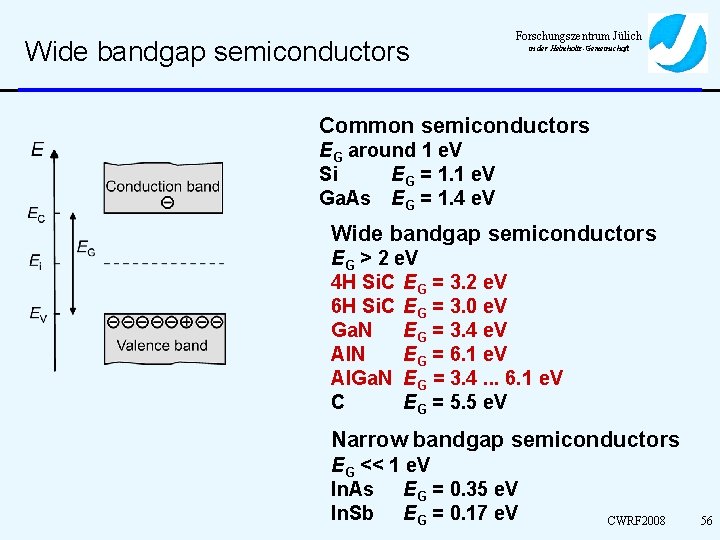
Wide bandgap semiconductors Forschungszentrum Jülich in der Helmholtz-Gemeinschaft Common semiconductors EG around 1 e. V Si EG = 1. 1 e. V Ga. As EG = 1. 4 e. V Wide bandgap semiconductors EG > 2 e. V 4 H Si. C EG = 3. 2 e. V 6 H Si. C EG = 3. 0 e. V Ga. N EG = 3. 4 e. V Al. N EG = 6. 1 e. V Al. Ga. N EG = 3. 4. . . 6. 1 e. V C EG = 5. 5 e. V Narrow bandgap semiconductors EG << 1 e. V In. As EG = 0. 35 e. V In. Sb EG = 0. 17 e. V CWRF 2008 56

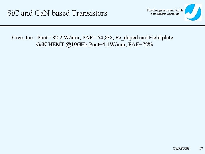
Si. C and Ga. N based Transistors Forschungszentrum Jülich in der Helmholtz-Gemeinschaft Cree, Inc : Pout= 32. 2 W/mm, PAE= 54, 8%, Fe_doped and Field plate Ga. N HEMT @10 GHz Pout=4. 1 W/mm, PAE=72% CWRF 2008 57

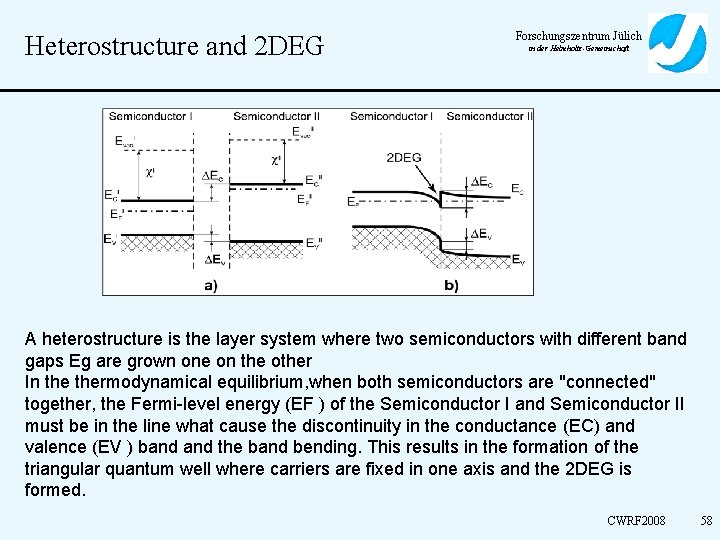
Heterostructure and 2 DEG Forschungszentrum Jülich in der Helmholtz-Gemeinschaft A heterostructure is the layer system where two semiconductors with different band gaps Eg are grown one on the other In thermodynamical equilibrium, when both semiconductors are "connected" together, the Fermi-level energy (EF ) of the Semiconductor I and Semiconductor II must be in the line what cause the discontinuity in the conductance (EC) and valence (EV ) band the band bending. This results in the formation of the triangular quantum well where carriers are fixed in one axis and the 2 DEG is formed. CWRF 2008 58