Electronic memory logic devices Flip Flop Output Input



- Slides: 33

Electronic memory & logic devices

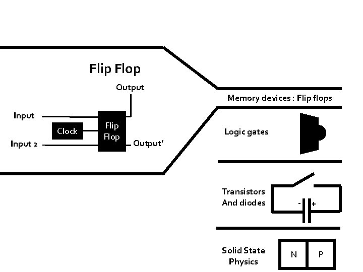
Flip Flop Output Input 2 Flip Flop Logic gates Output’ Transistors And diodes Solid State Physics - Clock N + Input Memory devices : Flip flops P

Transistors

Abstract Transistors have six salient features. First, they rapidly switch between two states in response to an input signal. Second, a small input voltage can control a large output voltage. Third, voltage is the common I/O signal carrier. Fourth, wires are the common interconnect. Fifth, common I/O and wires enable addressable signals, which means specific connections between devices. Sixth, amplification and addressable signals enables restoration, because the output voltage greatly exceeds the voltage necessary to control a downstream transistor.

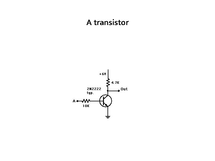
A transistor

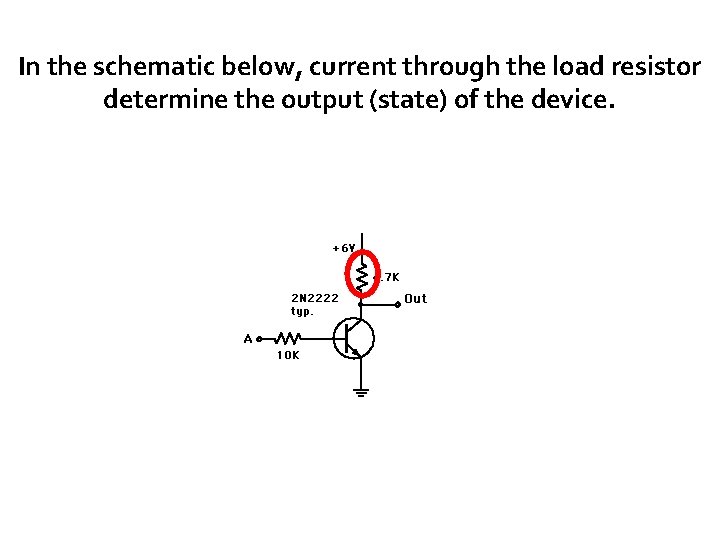
In the schematic below, current through the load resistor determine the output (state) of the device.

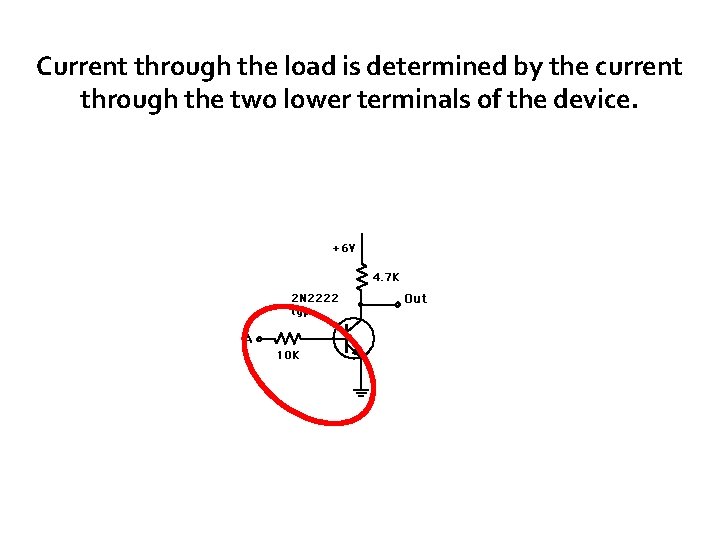
Current through the load is determined by the current through the two lower terminals of the device.

The current through the two lower terminals of the device is non-linearly responsive to the input voltage.

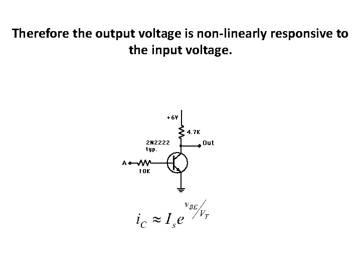
Therefore the output voltage is non-linearly responsive to the input voltage.

Logic gates

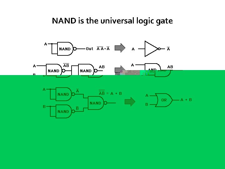
Abstract Transistors can be assembled into devices that render Boolean logic functions. The input and output voltages represent logic 0 or 1. NAND is the universal logic gate, and underpins design of higher level memory devices like latches and flip-flops.

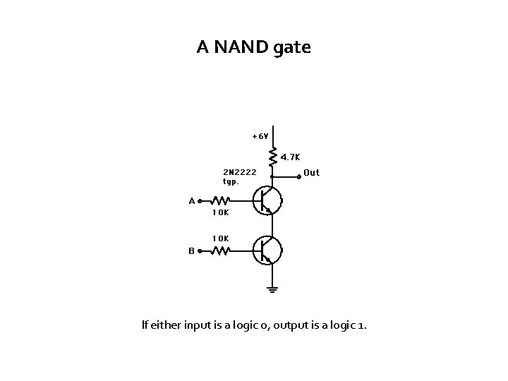
A NAND gate If either input is a logic 0, output is a logic 1.

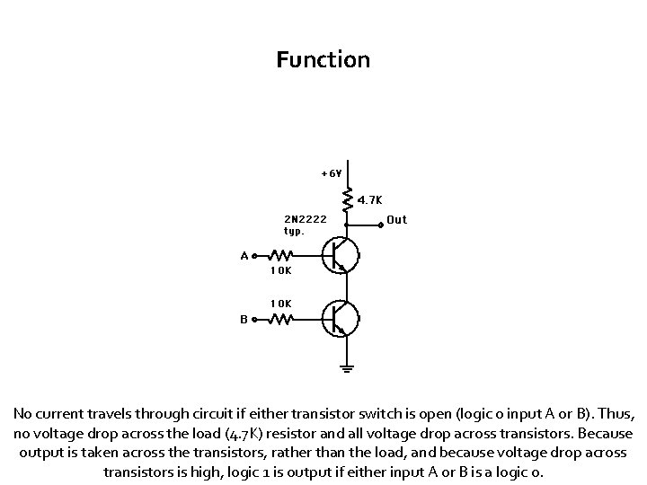
Function No current travels through circuit if either transistor switch is open (logic 0 input A or B). Thus, no voltage drop across the load (4. 7 K) resistor and all voltage drop across transistors. Because output is taken across the transistors, rather than the load, and because voltage drop across transistors is high, logic 1 is output if either input A or B is a logic 0.

NAND is the universal logic gate

Latches

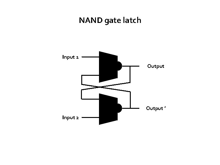
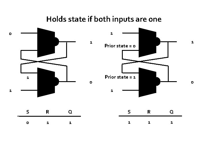
Abstract NAND gate latch, implemented in flip-flops, is a simple memory device that will latch onto an output state when both inputs are one. If zero is input, the latch output is 1, independent of prior state. The latch will hold state if both inputs are equal to 1.

NAND gate latch Input 1 Output ’ Input 2

Holds state if both inputs are one 1 0 1 Prior state = 0 Prior state = 1 0 1 1 S R Q 0 1 1 1

D-type flip-flops

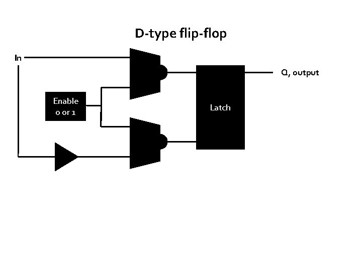
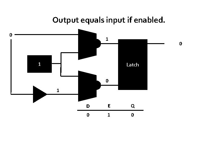
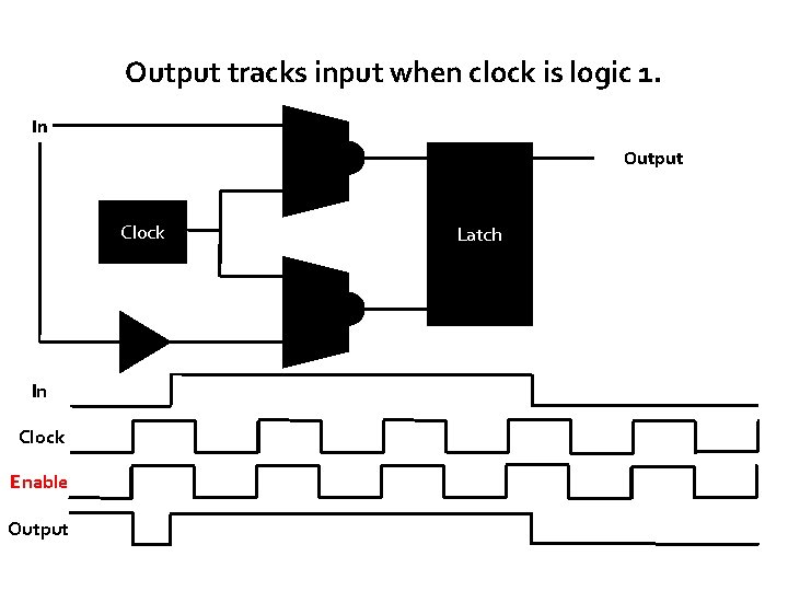
Abstract D-flip flop implements a NAND gate latch. The flip-flop output equals the Input, if enabled. The enable can be a clock. In this case, the output tracks the input when the clock is a logic 1.

D-type flip-flop In Q, output Enable 0 or 1 Latch

Output equals input if enabled. 0 1 1 0 Latch 0 1 D E Q 0 1 0

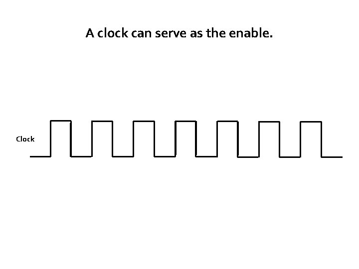
A clock can serve as the enable. Clock

Output tracks input when clock is logic 1. In Output Clock In Clock Enable Output Latch

JK-type flip-flops

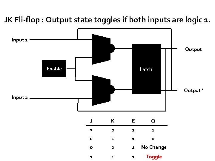
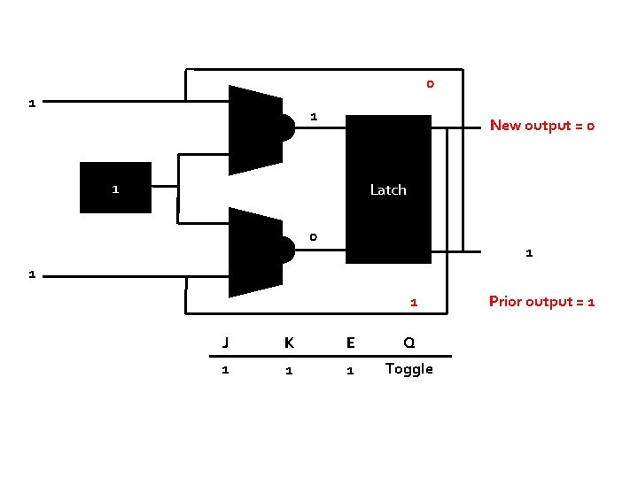
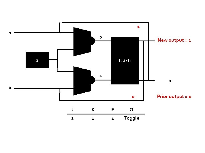
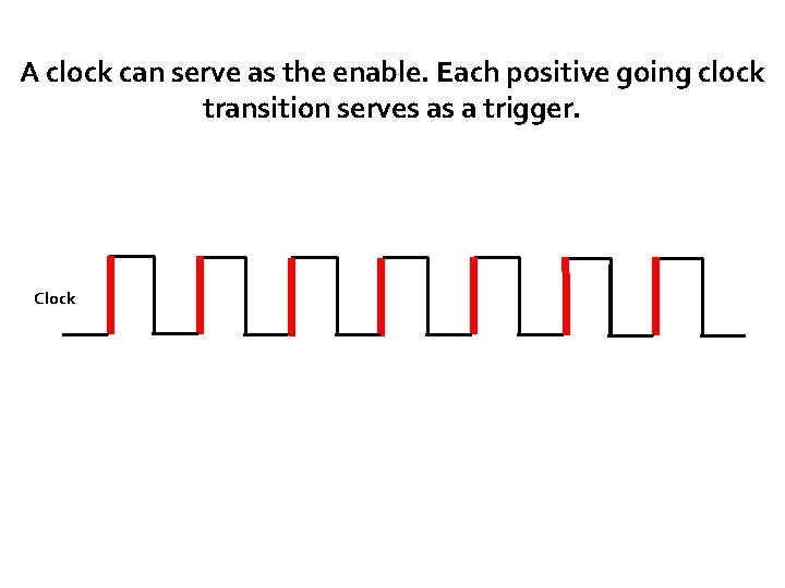
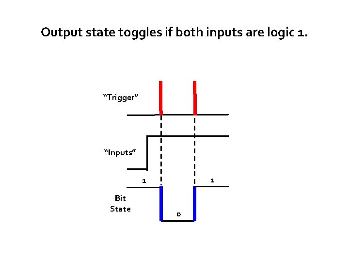
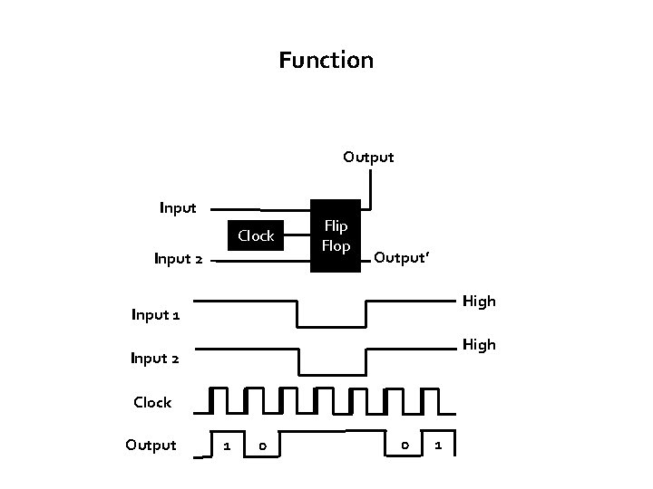
Abstract JK flip-flops also implement latches. Because of feedback, this flip-flop architecture will toggle output states when both inputs are logic 1. The enable can be a clock. In this case, the state of the flip-flop will toggle at the positive going transition of the clock, if both input are logic 1. Flip-flops have at least four salient features that admit well to implementation in systems. They perform fast computation. They have a consistent definition for logic 0 and 1. They perform the same function independent of their position (context) within a circuit. They have common interconnect and I/O signal carrier, which enable programming via specific device connections.

JK Fli-flop : Output state toggles if both inputs are logic 1. Input 1 Output Enable Latch Output ’ Input 2 J K E Q 1 0 1 1 0 0 0 1 No Change 1 1 1 Toggle

0 1 1 New output = 0 1 Latch 0 1 1 1 J K E Q 1 1 1 Toggle Prior output = 1

1 1 0 New output = 1 1 Latch 1 0 J K E Q 1 1 1 Toggle Prior output = 0

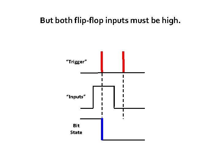
A clock can serve as the enable. Each positive going clock transition serves as a trigger. Clock

Output state toggles if both inputs are logic 1. “Trigger” “Inputs” 1 1 Bit State 0

But both flip-flop inputs must be high. “Trigger” “Inputs” Bit State

Function Output Input Clock Input 2 Flip Flop Output’ High Input 1 High Input 2 Clock Output 1 0 0 1