Sequential Logic Types of digital systems 1 Combinational
Sequential Logic
Types of digital systems 1) Combinational logic circuits : 2) Sequential logic circuits: n In Combinational logic circuits, where the output of combination circuit at any instant of time, depends only on the levels present at input terminal. n Combinational logic circuits do not use any memory. n Hence the previous state of input does not have any affect on the present state of the circuit.
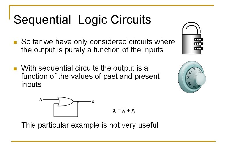
Sequential Logic Circuits n n So far we have only considered circuits where the output is purely a function of the inputs With sequential circuits the output is a function of the values of past and present inputs X=X+A This particular example is not very useful 1 7 3
Sequential Circuits - Aims q q The output of a sequential circuit depends on the present input & the previous output & the sequence in which the inputs are applied. In order to provide the previous input or output a memory element is required to be used. Thus a sequential circuit needs memory element. q Also required clock input. q Examples are flip-flops, counter, shift register.
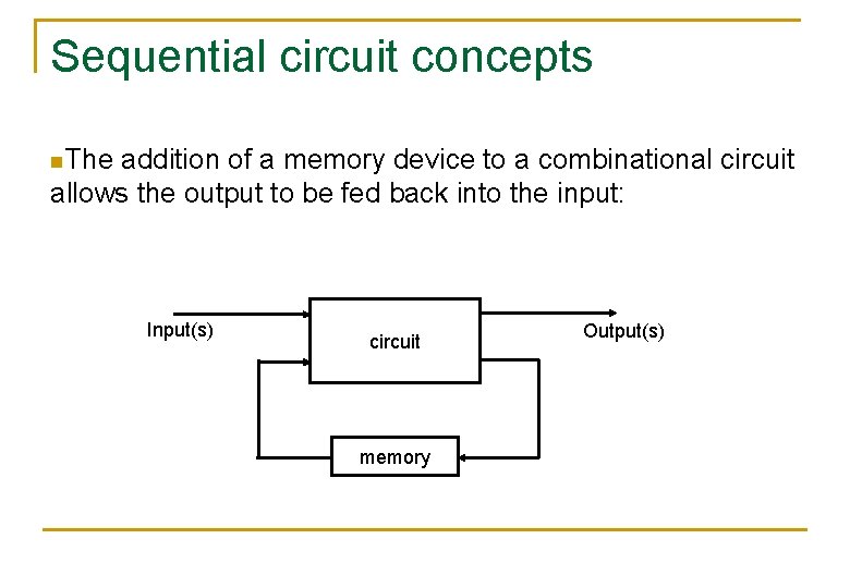
Sequential circuit concepts n. The addition of a memory device to a combinational circuit allows the output to be fed back into the input: Input(s) circuit memory Output(s)
States n n n Present state : -the data stored by the memory element at any instant of time is called as the present state i. e Qn, Qn’. Next state: -the ckt operates on the external inputs and present state to provide new output, new output stored in the memory elements & it is called as next state i. e. Qn+1, Qn+1’. Clock signal: - it is a timing signal. Its have leading or positive or rising edge & trailing or falling or negative edge.
Sequential circuits 1) Synchronous Sequential circuits 2) Asynchronous Sequential circuits n n n In Synchronous Sequential circuits: the state of memory element is affected only if the input changed. Slower because of the delay. A clocked flip-flop acts as a memory element. These circuits are easy to design.
In Asynchronous Sequential circuits n n The state of memory element will change any time as soon as the input changed. Faster because clock is not present. An un-clocked flip-flop or time delay elements acts as a memory element. These circuits are difficult to design. LATCH: - the latch is a types of temporary starage device which has two stable states.
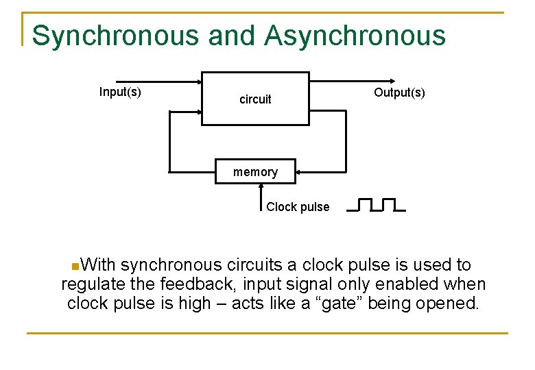
Synchronous and Asynchronous Input(s) circuit Output(s) memory Clock pulse n. With synchronous circuits a clock pulse is used to regulate the feedback, input signal only enabled when clock pulse is high – acts like a “gate” being opened.
Flip Flops n n SR Type Flip Flops D Type Flip Flops T Type Flip Flops J-K Type Flip Flops
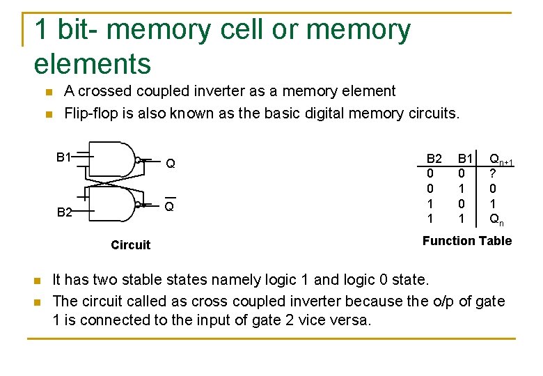
1 bit- memory cell or memory elements n n A crossed coupled inverter as a memory element Flip-flop is also known as the basic digital memory circuits. B 1 Q B 2 Q Circuit n n B 2 0 0 1 1 B 1 0 1 Qn+1 ? 0 1 Qn Function Table It has two stable states namely logic 1 and logic 0 state. The circuit called as cross coupled inverter because the o/p of gate 1 is connected to the input of gate 2 vice versa.
operations n n n Assume that the o/p of gate 1, Q=1 hence B 2 = 1. As B 2=1 than gate 2 o/p is 0 i. e Q = 0 hennce B 1=0. The o/p of ckt Q & Q will always be complimentary that means Q=1, Q=0, & vice versa. They will never be qual to Q = Q= 0 OR 1 ia an invalid state. The ckt has two stable state i. e. Q=1, OR Q= 0 i. e set states, another is Q=0 OR Q= 1 i. e. reset states.
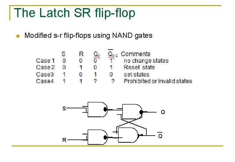
The Latch SR flip-flop n Modified s-r flip-flops using NAND gates S R Q Q
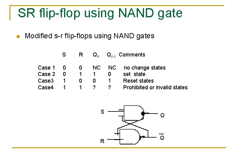
SR flip-flop using NAND gate n Modified s-r flip-flops using NAND gates Case 1 Case 2 Case 3 Case 4 S R Qn Qn c Comments 0 0 1 1 0 1 NC 1 0 ? NC 0 1 ? S R no change states set state Reset states Prohibited or invalid states Q Q
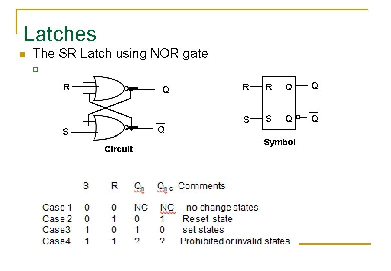
Latches n The SR Latch using NOR gate q R Q R R Q Q S S Q Q Q S Symbol Circuit Function Table
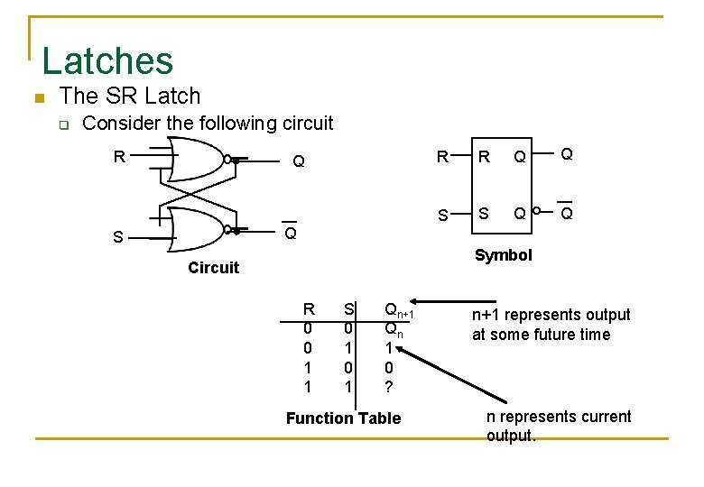
Latches n The SR Latch q Consider the following circuit R Q R R Q Q S S Q Q Q S Symbol Circuit R 0 0 1 1 S 0 1 Qn+1 Qn 1 0 ? Function Table n+1 represents output at some future time n represents current output.
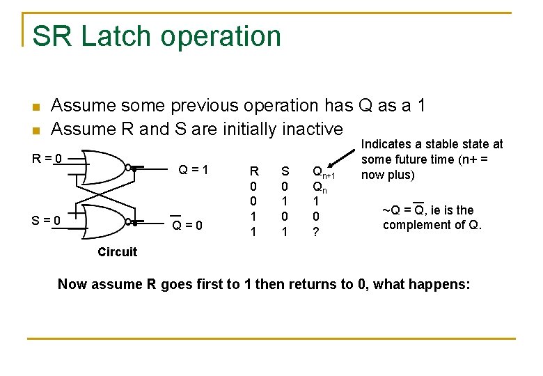
SR Latch operation n n Assume some previous operation has Q as a 1 Assume R and S are initially inactive R=0 Q=1 S=0 Q=0 R 0 0 1 1 S 0 1 Qn+1 Qn 1 0 ? Indicates a stable state at some future time (n+ = now plus) ~Q = Q, ie is the complement of Q. Circuit Now assume R goes first to 1 then returns to 0, what happens:
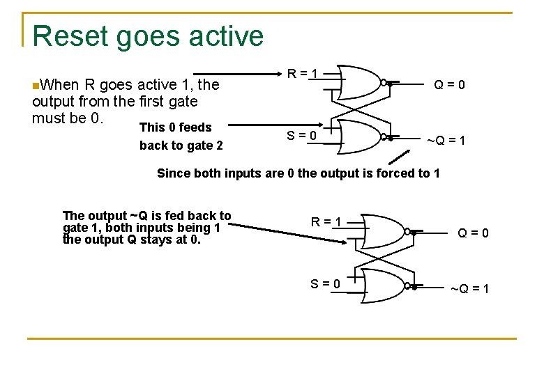
Reset goes active n. When R goes active 1, the output from the first gate must be 0. This 0 feeds back to gate 2 R=1 S=0 Q=0 ~Q = 1 Since both inputs are 0 the output is forced to 1 The output ~Q is fed back to gate 1, both inputs being 1 the output Q stays at 0. R=1 S=0 Q=0 ~Q = 1
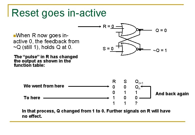
Reset goes in-active R=0 R now goes inactive 0, the feedback from ~Q (still 1), holds Q at 0. Q=0 n. When S=0 ~Q = 1 The “pulse” in R has changed the output as shown in the function table: We went from here To here R 0 0 1 1 S 0 1 Qn+1 Qn 1 0 ? And back again In that process, Q changed from 1 to 0. Further signals on R will have no effect.
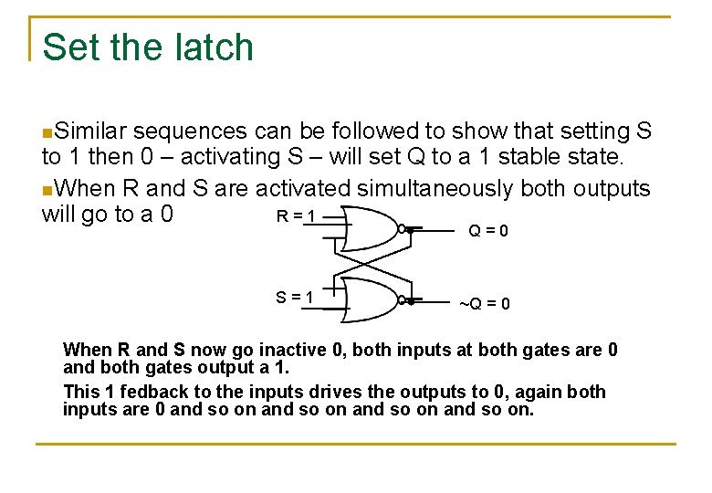
Set the latch n. Similar sequences can be followed to show that setting S to 1 then 0 – activating S – will set Q to a 1 stable state. n. When R and S are activated simultaneously both outputs will go to a 0 R=1 Q=0 S=1 ~Q = 0 When R and S now go inactive 0, both inputs at both gates are 0 and both gates output a 1. This 1 fedback to the inputs drives the outputs to 0, again both inputs are 0 and so on.
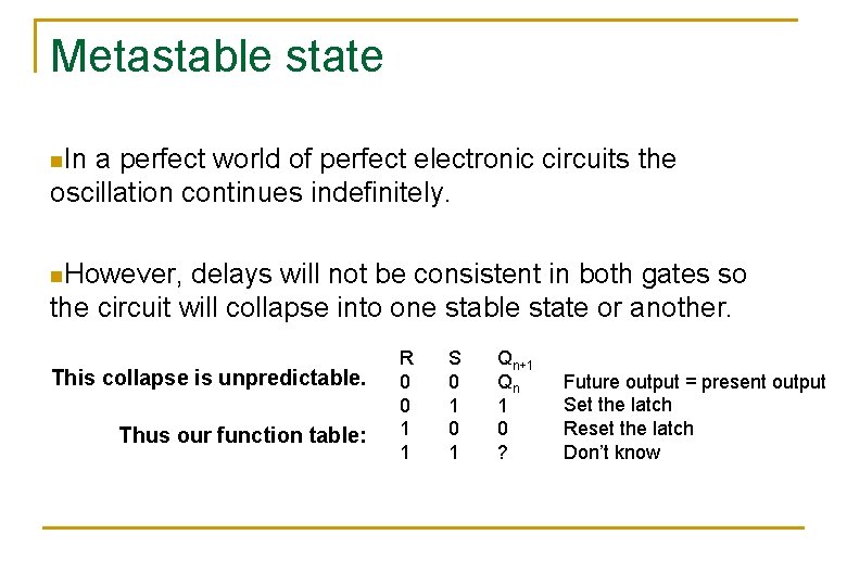
Metastable state n. In a perfect world of perfect electronic circuits the oscillation continues indefinitely. n. However, delays will not be consistent in both gates so the circuit will collapse into one stable state or another. This collapse is unpredictable. Thus our function table: R 0 0 1 1 S 0 1 Qn+1 Qn 1 0 ? Future output = present output Set the latch Reset the latch Don’t know
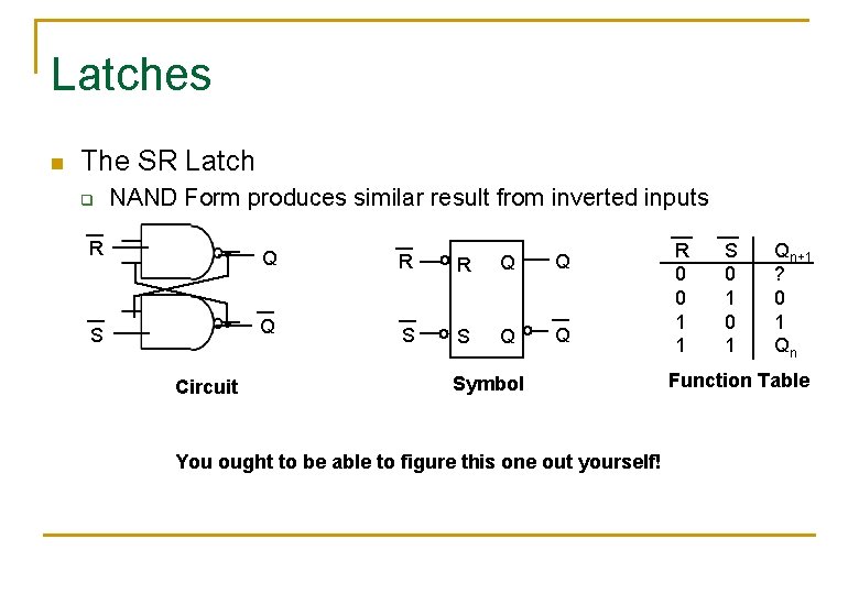
Latches n The SR Latch q NAND Form produces similar result from inverted inputs R Q R R Q Q S S Q Q Circuit Symbol You ought to be able to figure this one out yourself! R 0 0 1 1 S 0 1 Qn+1 ? 0 1 Qn Function Table
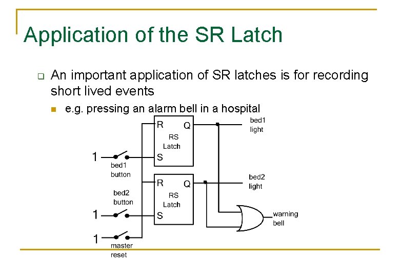
Application of the SR Latch q An important application of SR latches is for recording short lived events n e. g. pressing an alarm bell in a hospital
Triggering method n n n Two types of triggering method 1) Level triggering 2) Edge triggering
Level triggering n n Two types : 1) Positive Level triggering 2) Negative Level triggering When the flip-flop is triggered the positive or negative voltage clock pulse to change its output state i. e. set or reset is called level triggering.
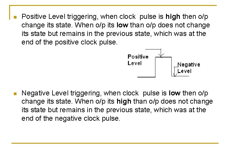
n Positive Level triggering, when clock pulse is high then o/p change its state. When o/p its low than o/p does not change its state but remains in the previous state, which was at the end of the positive clock pulse. n Negative Level triggering, when clock pulse is low then o/p change its state. When o/p its high than o/p does not change its state but remains in the previous state, which was at the end of the negative clock pulse.
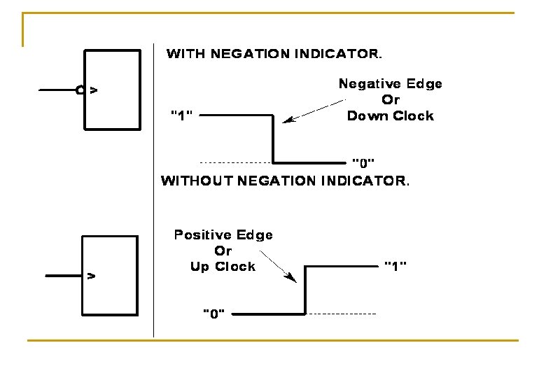
Edge triggering n n Two types : 1) Positive Edge triggering 2) Negative Edge triggering : - o/p of flip-flop change according to input during either of positive or negative edge of clock input.
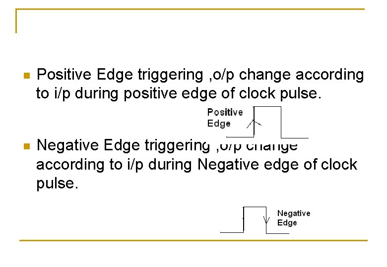
n Positive Edge triggering , o/p change according to i/p during positive edge of clock pulse. n Negative Edge triggering , o/p change according to i/p during Negative edge of clock pulse.
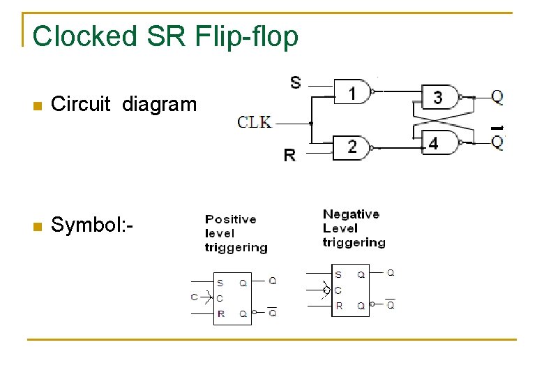
Clocked SR Flip-flop n Circuit diagram n Symbol: -
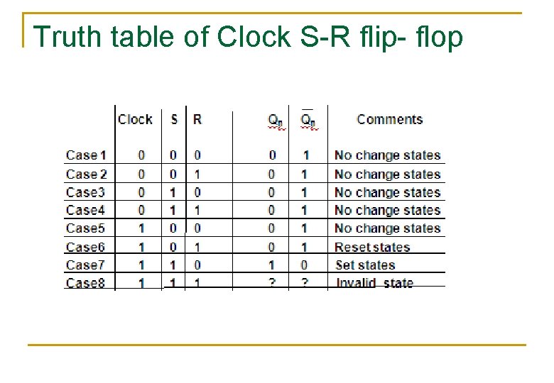
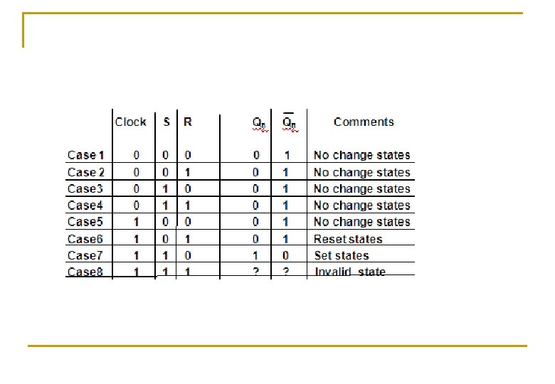
Truth table of Clock S-R flip- flop
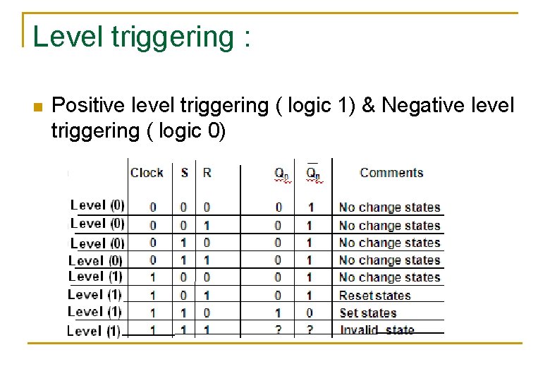
Level triggering : n Positive level triggering ( logic 1) & Negative level triggering ( logic 0)
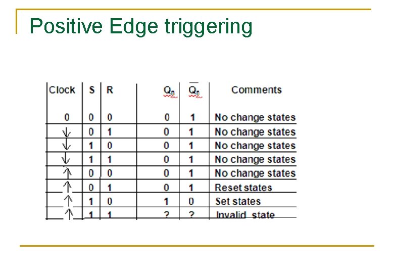
Positive Edge triggering
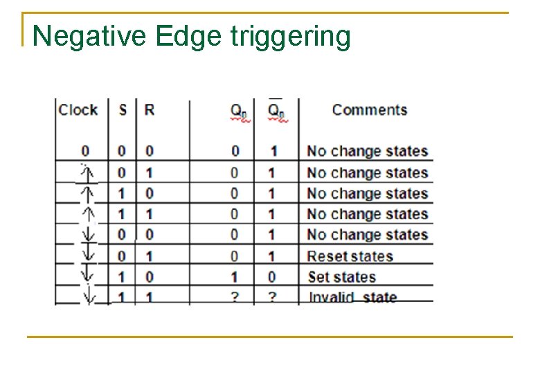
Negative Edge triggering
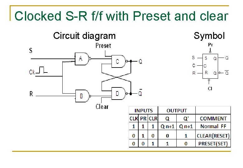
Clocked S-R f/f with Preset and clear Circuit diagram Symbol
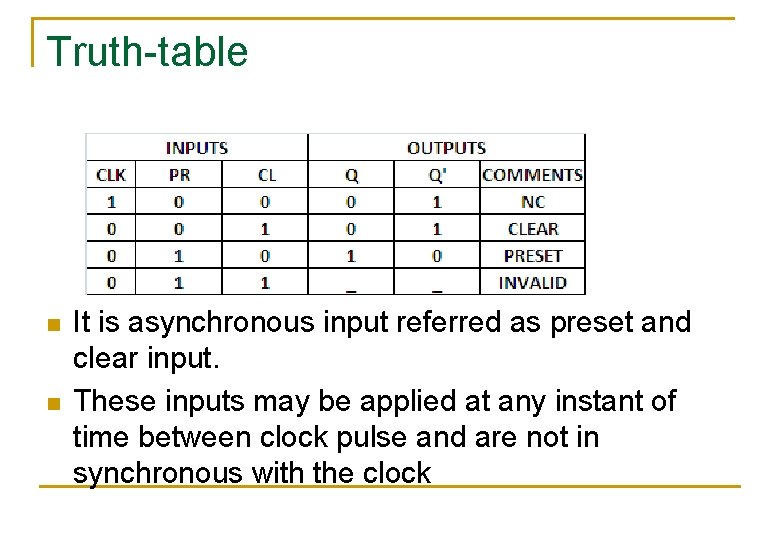
Truth-table n n It is asynchronous input referred as preset and clear input. These inputs may be applied at any instant of time between clock pulse and are not in synchronous with the clock
Drawback of S-R F/F n n n When S=R=1 & S=R=0 then o/p of Q & Q either don’t change or no change or they are invalid due to race around condition. This disadvantages overcome by using the D flipflop. Application : - SR F/F used in Electronic timer.
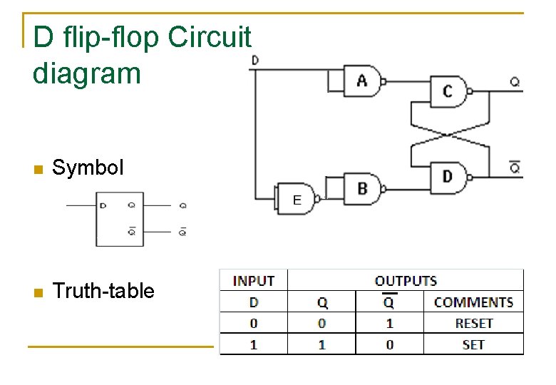
D flip-flop Circuit diagram n Symbol n Truth-table
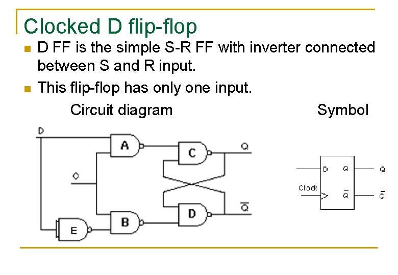
Clocked D flip-flop n n D FF is the simple S-R FF with inverter connected between S and R input. This flip-flop has only one input. Circuit diagram Symbol
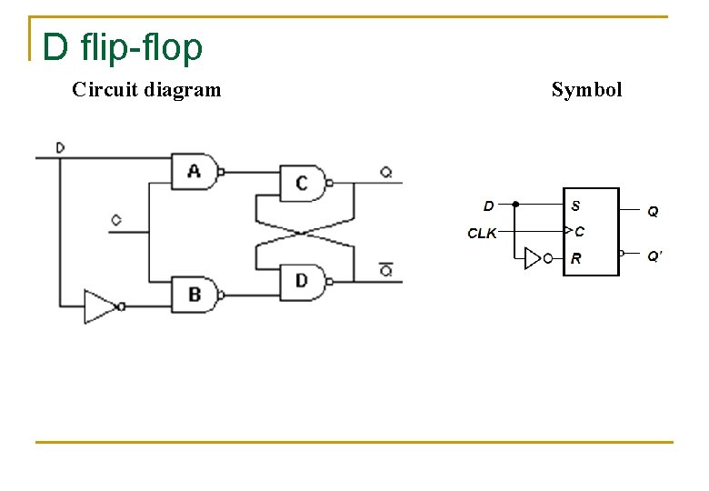
D flip-flop Circuit diagram Symbol
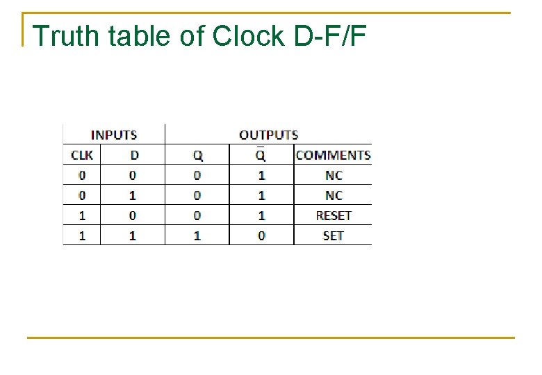
Truth table of Clock D-F/F
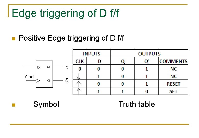
Edge triggering of D f/f n n Positive Edge triggering of D f/f Symbol Truth table
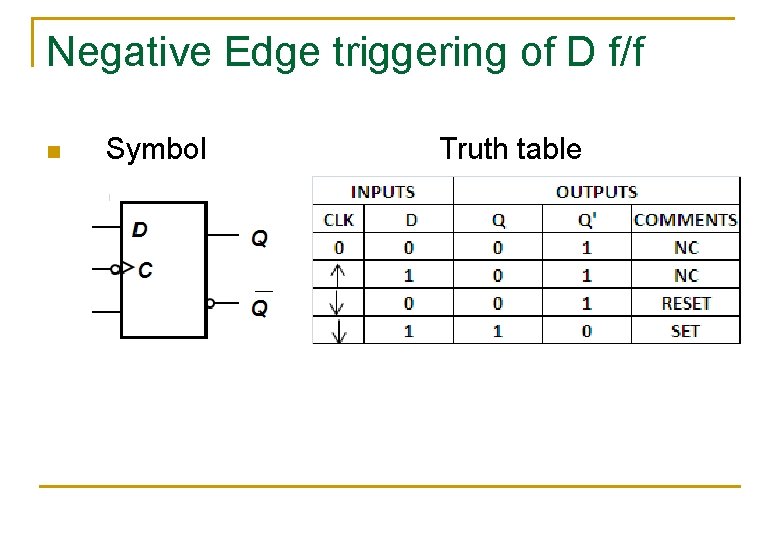
Negative Edge triggering of D f/f n Symbol Truth table
Dflip-flop n n n Application: Parallel data transfer. Delay elements In digital latch.
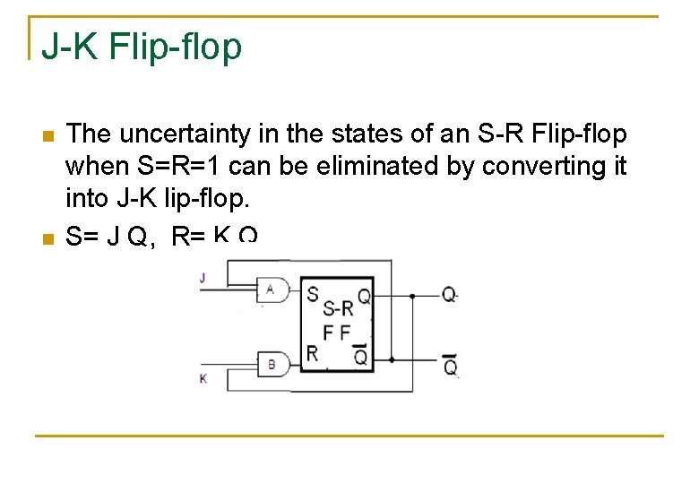
J-K Flip-flop n n The uncertainty in the states of an S-R Flip-flop when S=R=1 can be eliminated by converting it into J-K lip-flop. S= J Q, R= K Q
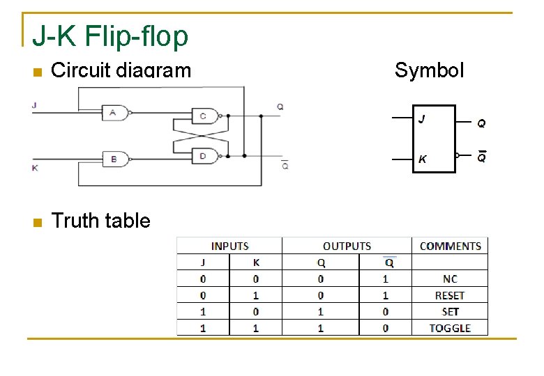
J-K Flip-flop n Circuit diagram n Truth table Symbol
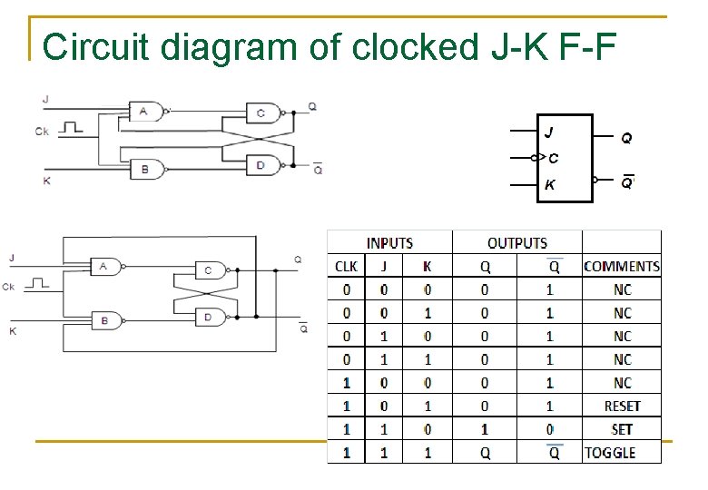
Circuit diagram of clocked J-K F-F
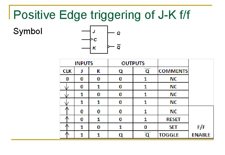
Positive Edge triggering of J-K f/f Symbol
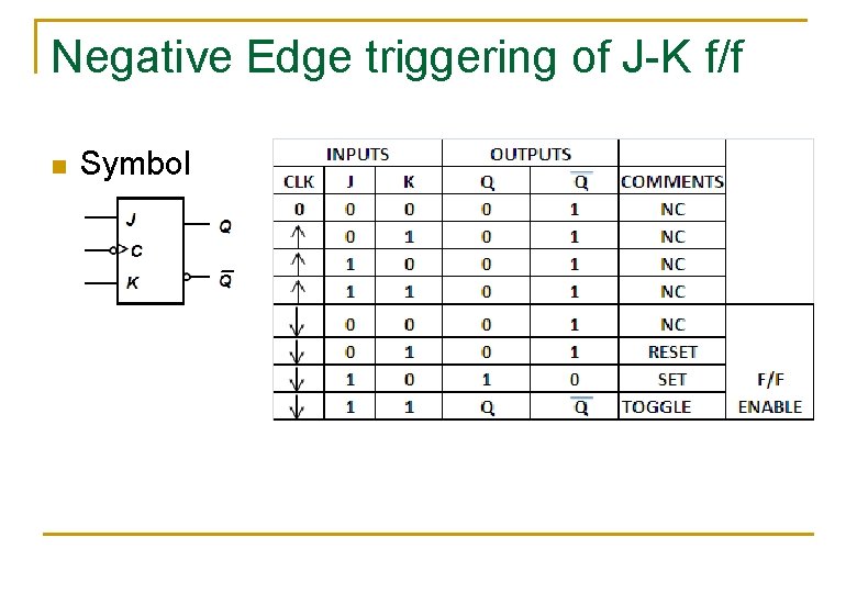
Negative Edge triggering of J-K f/f n Symbol
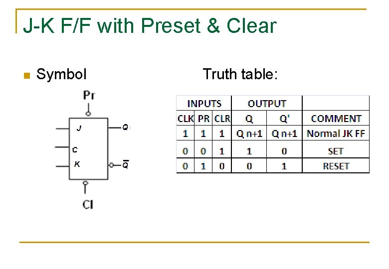
J-K F/F with Preset & Clear n Symbol Truth table:
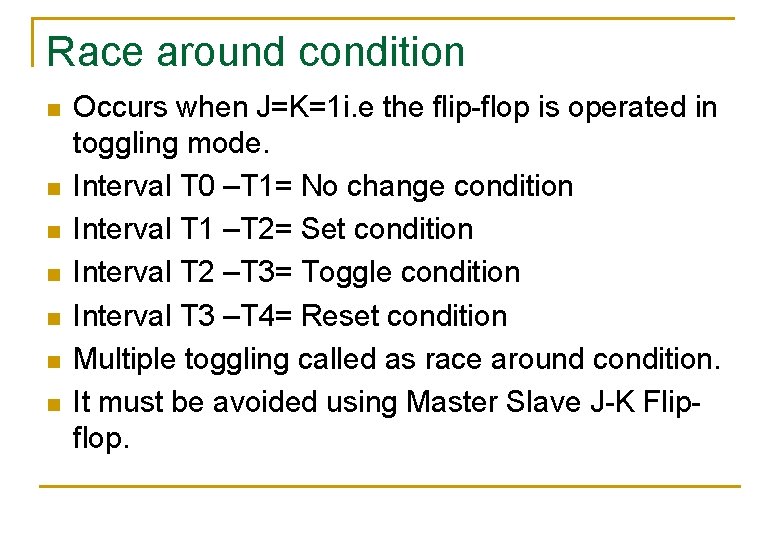
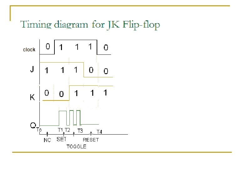
Race around condition n n n Occurs when J=K=1 i. e the flip-flop is operated in toggling mode. Interval T 0 –T 1= No change condition Interval T 1 –T 2= Set condition Interval T 2 –T 3= Toggle condition Interval T 3 –T 4= Reset condition Multiple toggling called as race around condition. It must be avoided using Master Slave J-K Flipflop.
Application: n n Shift Register Counter
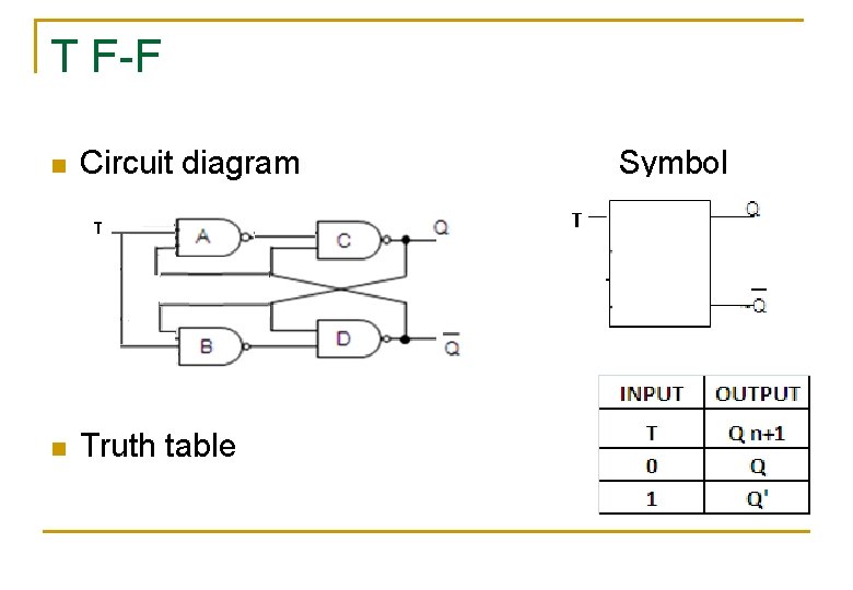
T F-F n Circuit diagram n Truth table Symbol

Clocked T FF n Circuit diagram Symbol
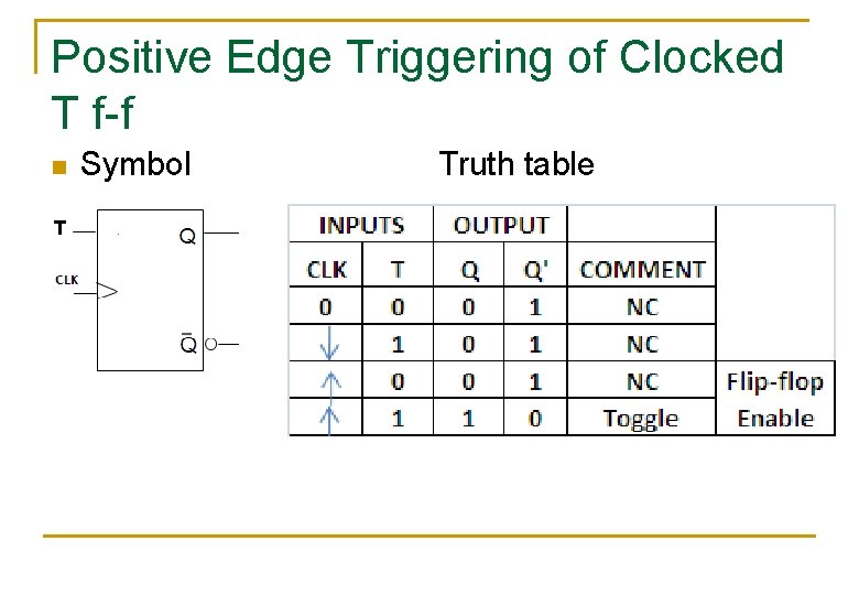
Positive Edge Triggering of Clocked T f-f n Symbol Truth table
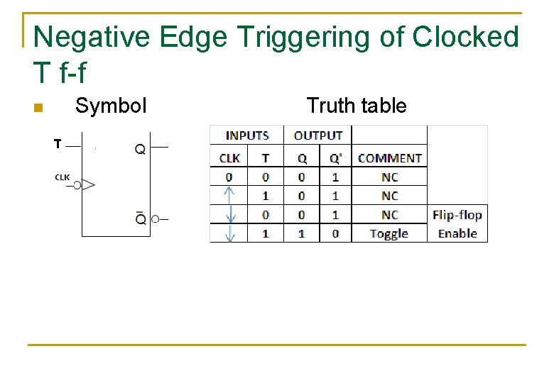
Negative Edge Triggering of Clocked T f-f n Symbol Truth table
Application of T FF n n Frequency division Ripple counter
Master slave J-K FF
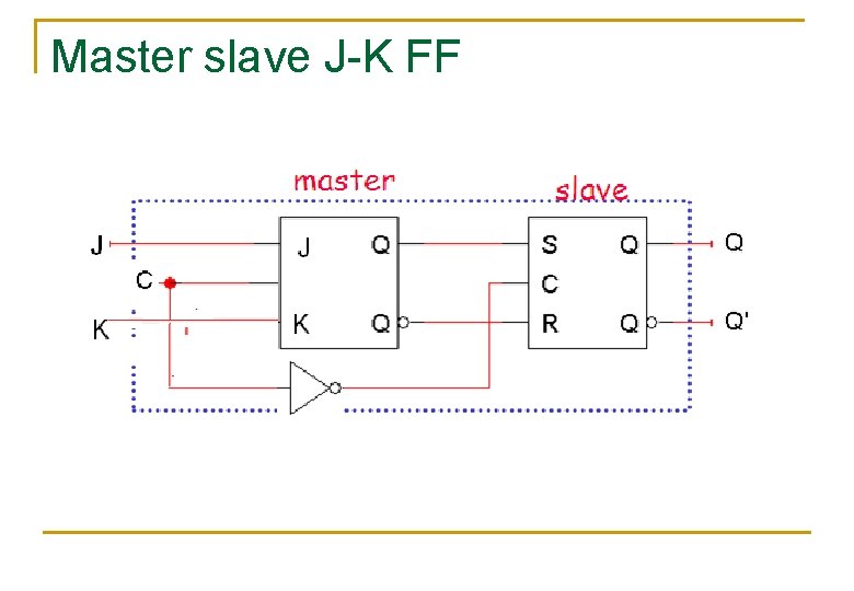
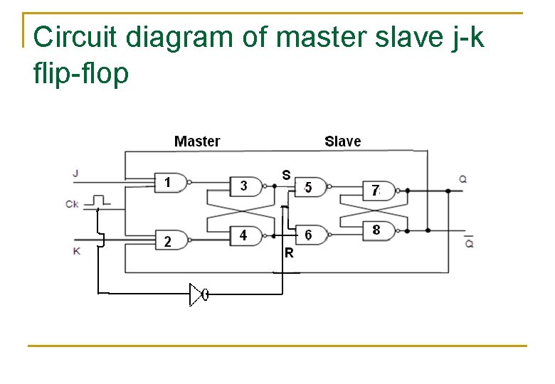
Operation of MSJK F-F n n n Its combination of clocked J-K F-F & Clocked S-R -F-F. Where clocked J-K F-F acts as Master & Clocked S-R-F-F acts as Slave. Master is positive level triggering i. e clock=1 & slave is negative level triggering i. e clock=1
Circuit diagram of master slave j-k flip-flop
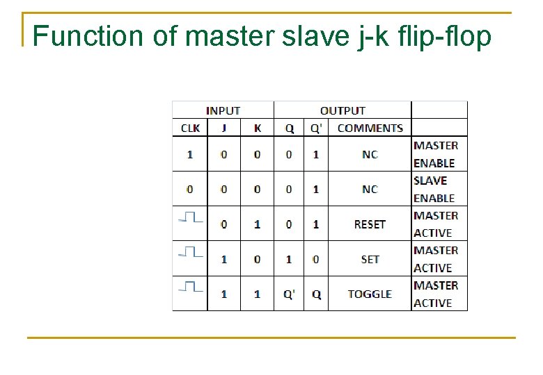
Function of master slave j-k flip-flop
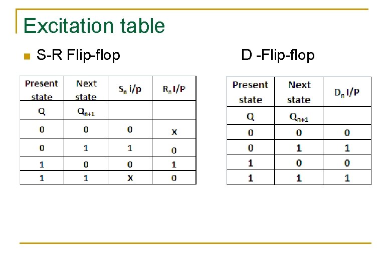
Excitation table n S-R Flip-flop D -Flip-flop
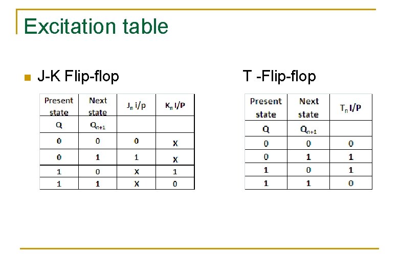
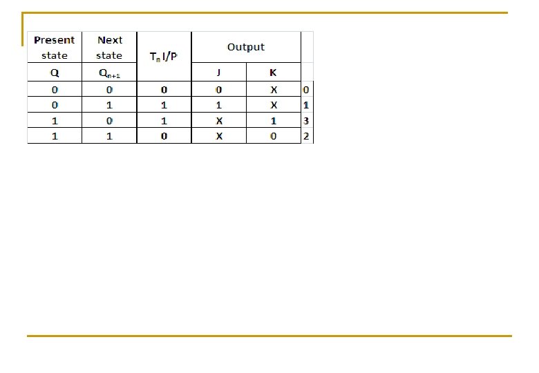
Excitation table n J-K Flip-flop T -Flip-flop
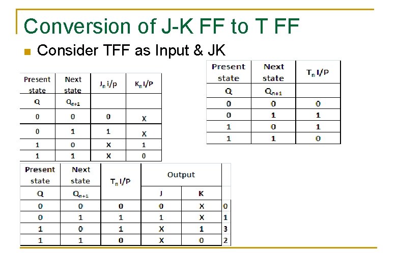
Conversion of J-K FF to T FF n Consider TFF as Input & JK


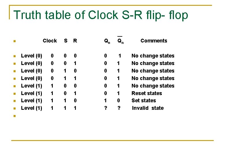
Truth table of Clock S-R flip- flop Clock n n n n n Level (0) Level (1) 0 0 1 1 S R Qn Qn Comments 0 0 1 1 0 1 0 1 0 0 0 1 ? 1 1 1 0 ? No change states No change states Reset states Set states Invalid state
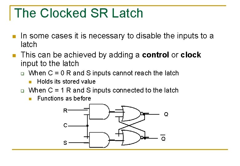
The Clocked SR Latch n n In some cases it is necessary to disable the inputs to a latch This can be achieved by adding a control or clock input to the latch q When C = 0 R and S inputs cannot reach the latch n q Holds its stored value When C = 1 R and S inputs connected to the latch n Functions as before R Q C S Q
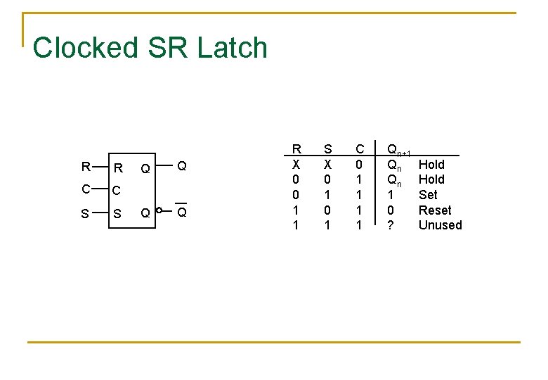
Clocked SR Latch R R C C S S Q Q R X 0 0 1 1 S X 0 1 C 0 1 1 Qn+1 Qn Qn 1 0 ? Hold Set Reset Unused
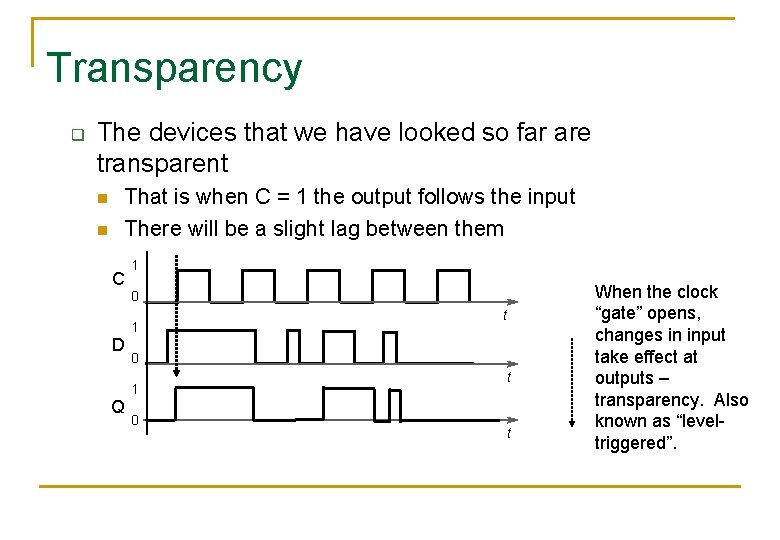
Transparency q The devices that we have looked so far are transparent n n That is when C = 1 the output follows the input There will be a slight lag between them C 1 0 1 D 0 1 Q t 0 t t When the clock “gate” opens, changes in input take effect at outputs – transparency. Also known as “leveltriggered”.
Propagation Delay, set-up and hold (for transparent circuits) n. Propagation delay: n. Time taken for any change at inputs to affect outputs (change on D to change on Q). n. Setup time: n. Data on inputs D must be held steady for at least this time before the clock changes. n. Hold time: n. Data on inputs D must be held steady for at least this time after the clock changes.
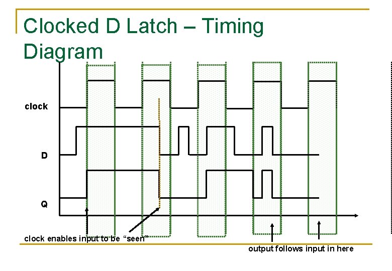
Clocked D Latch – Timing Diagram clock D Q clock enables input to be “seen” output follows input in here
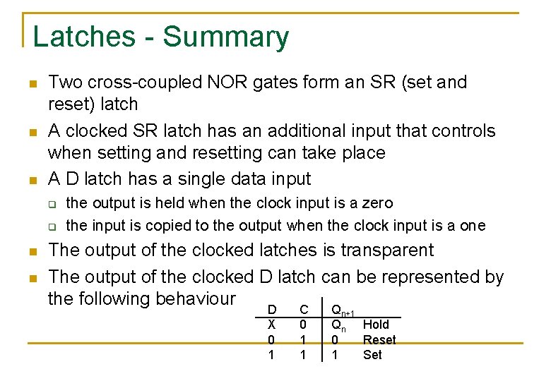
Latches - Summary n n n Two cross-coupled NOR gates form an SR (set and reset) latch A clocked SR latch has an additional input that controls when setting and resetting can take place A D latch has a single data input q q n n the output is held when the clock input is a zero the input is copied to the output when the clock input is a one The output of the clocked latches is transparent The output of the clocked D latch can be represented by the following behaviour D C Q X 0 1 1 n+1 Qn 0 1 Hold Reset Set
Latches and Flip Flops n. Terms are sometimes used confusingly: n. A latch is not clocked whereas a flip-flop is clocked. n. A clocked latch can therefore equally be referred to as a flip flop (SR flip flop, D flip flop). n. However, as we shall see, all practical flip flops are edge-triggered on the clock pulse. n. Sometimes latches are included within flip flops as a sub-type.
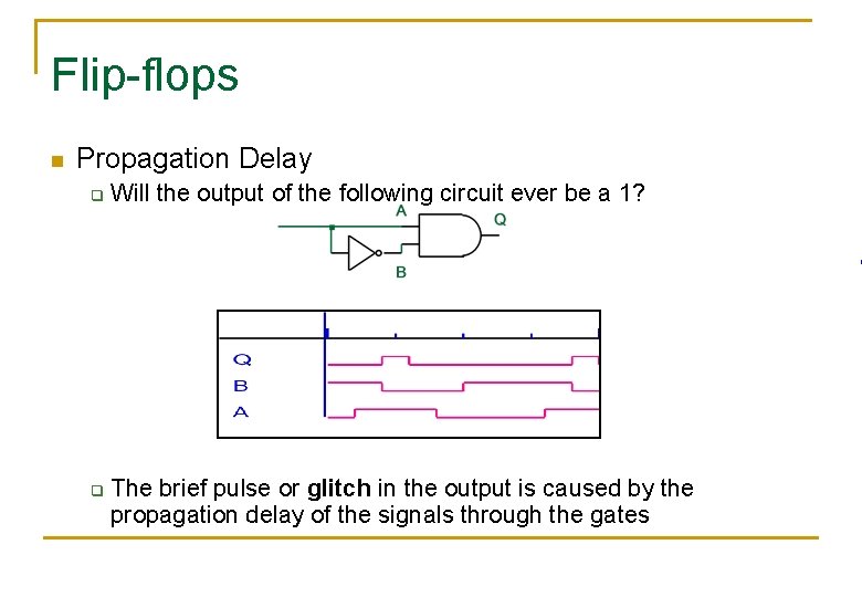
Flip-flops n Propagation Delay q q Will the output of the following circuit ever be a 1? The brief pulse or glitch in the output is caused by the propagation delay of the signals through the gates
Latches and Flip Flops n. Clocked latches are level triggered. While the clock is high, inputs and thus outputs can change. n. This is not always desirable. n. A Flip Flop is edge-triggered – either by the leading or falling edge of the clock pulse. n. Ideally, it responds to the inputs only at a particular instant in time. n. It is not transparent.
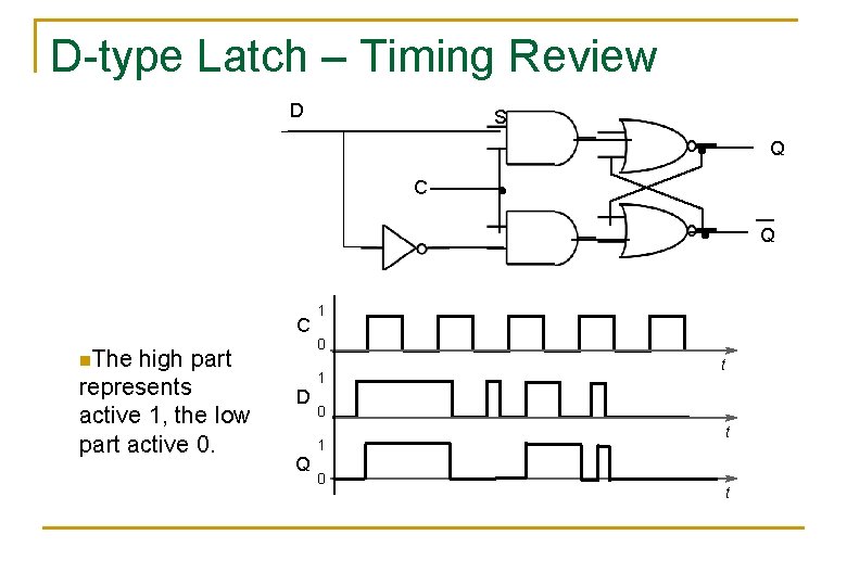
D-type Latch – Timing Review D S Q C n. The high part represents active 1, the low part active 0. 1 0 1 D 0 1 Q t 0 t t
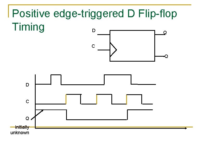
Positive edge-triggered D Flip-flop Timing D Q C ~Q D C Q initially unknown
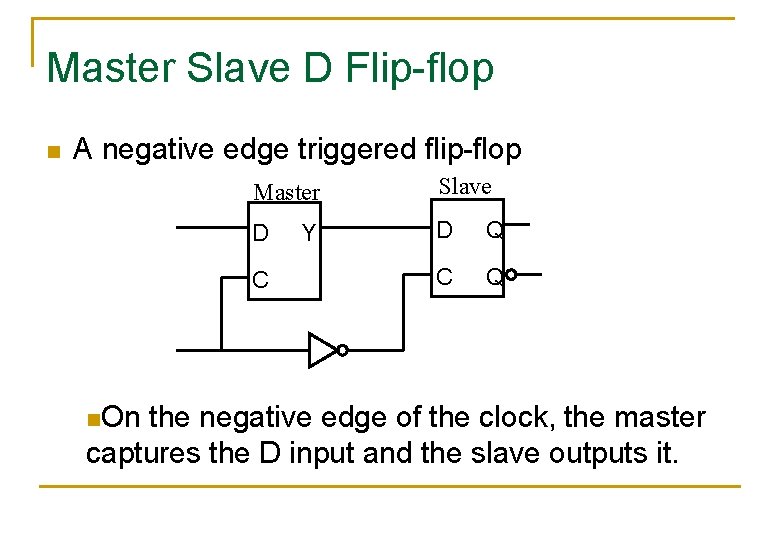
Master Slave D Flip-flop n A negative edge triggered flip-flop Master Slave D D Q C n. On Y the negative edge of the clock, the master captures the D input and the slave outputs it.
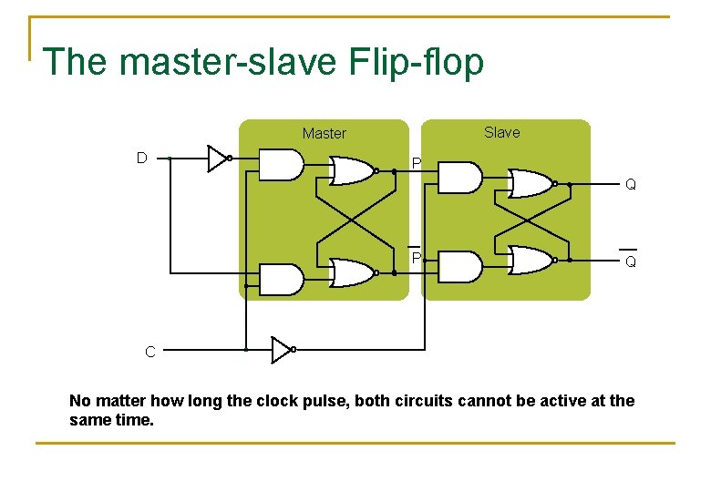
The master-slave Flip-flop Slave Master D P Q C No matter how long the clock pulse, both circuits cannot be active at the same time.
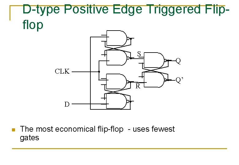
D-type Positive Edge Triggered Flipflop S Q CLK R D n The most economical flip-flop - uses fewest gates Q’
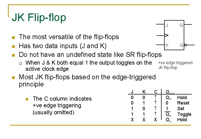
JK Flip-flop n n n The most versatile of the flip-flops Has two data inputs (J and K) Do not have an undefined state like SR flip-flops q n When J & K both equal 1 the output toggles on the active clock edge J Q K Q +ve edge triggered JK flip-flop Most JK flip-flops based on the edge-triggered principle n The C column indicates +ve edge triggering (usually omitted) J 0 0 1 1 X K 0 1 X C X Qn+1 Qn 0 1 Qn Qn Hold Reset Set Toggle Hold
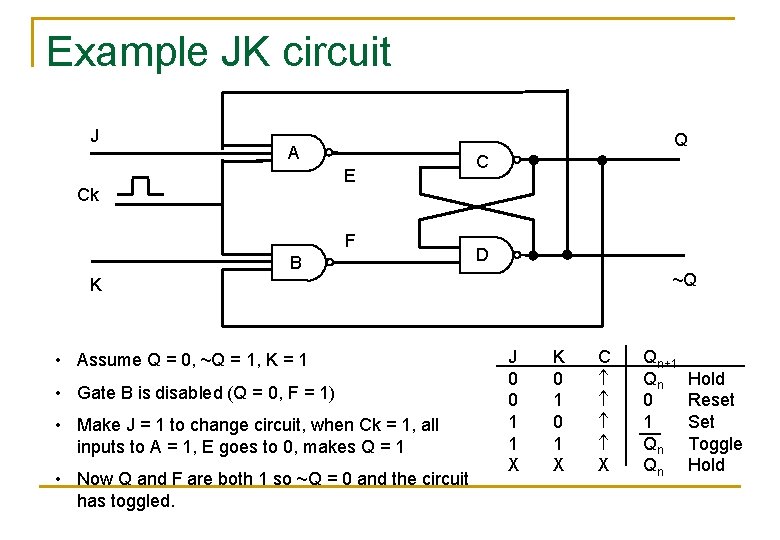
Example JK circuit J Q A E Ck F B C D ~Q K • Assume Q = 0, ~Q = 1, K = 1 • Gate B is disabled (Q = 0, F = 1) • Make J = 1 to change circuit, when Ck = 1, all inputs to A = 1, E goes to 0, makes Q = 1 • Now Q and F are both 1 so ~Q = 0 and the circuit has toggled. J 0 0 1 1 X K 0 1 X C X Qn+1 Qn 0 1 Qn Qn Hold Reset Set Toggle Hold
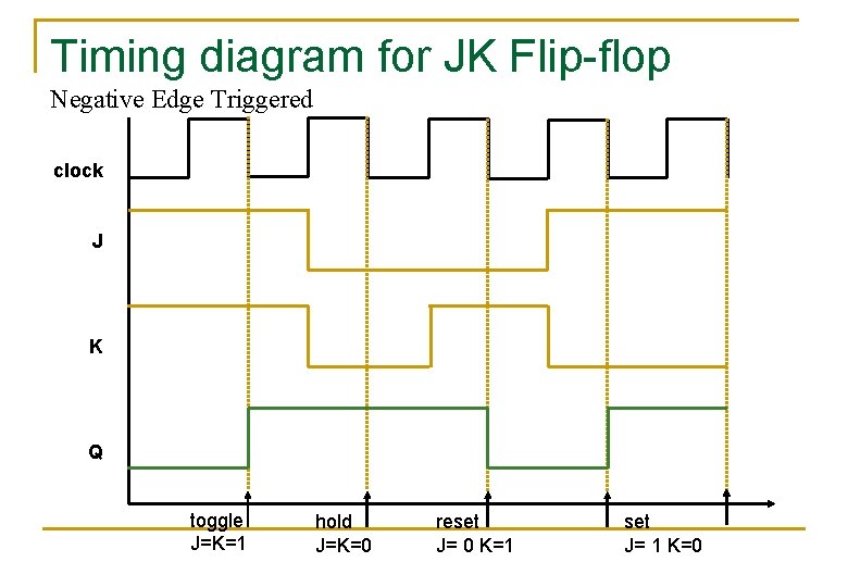
Timing diagram for JK Flip-flop Negative Edge Triggered clock J K Q toggle J=K=1 hold J=K=0 reset J= 0 K=1 set J= 1 K=0
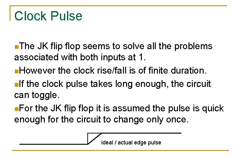
Clock Pulse n. The JK flip flop seems to solve all the problems associated with both inputs at 1. n. However the clock rise/fall is of finite duration. n. If the clock pulse takes long enough, the circuit can toggle. n. For the JK flip flop it is assumed the pulse is quick enough for the circuit to change only once. ideal / actual edge pulse
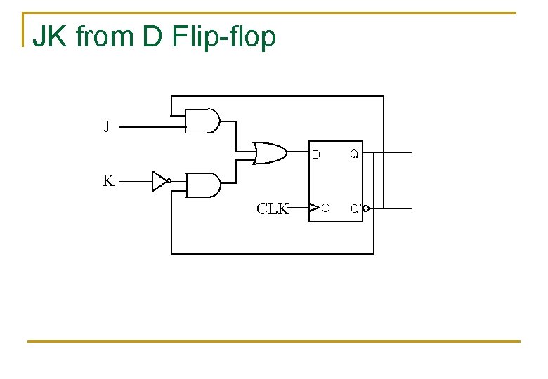
JK from D Flip-flop J Q D K CLK C Q’
Summary n. Flip flops are circuits controlled by a clock. n. Triggered on the edge of the pulse to avoid races with both inputs at 1 during the clock pulse. n. Because modern ic’s have a small propagation delay races can still occur. n. The master-slave configuration solves this problem by having only master or slave active at any one time.
What you should be able to do n. Explain the difference between combinational and sequential circuits n. Explain the basic operation of SR and D latches. n. Explain the operation of SR and JK flip flops. n. Explain the operation of master-slave flip flops. n. Draw simple timing diagrams for clocked latches and edge-triggered flip flops. n. Define setup and hold times for a transparent latch.
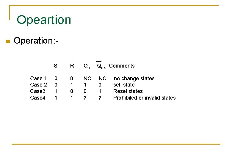
Opeartion n Operation: - Case 1 Case 2 Case 3 Case 4 S R Qn Qn c Comments 0 0 1 1 0 1 NC 1 0 ? NC 0 1 ? no change states set state Reset states Prohibited or invalid states
- Slides: 96