Efficient Computation methods for 3 D Microscopic Ellipsometry












- Slides: 65

Efficient Computation methods for 3 D Microscopic Ellipsometry Yia-Chung Chang Research Center for Applied Sciences (RCAS) Academia Sinica, Taipei, Taiwan, R. O. C. Collaborators: Huai-Yi Xie, Paul C. -H. Chien, Yu-Da Chen (RCAS, AS) R. Moirangthem, Shih-Hsin Hsu IWCSW, NTU, Oct. 17, 2013 1

Introduction • Targeted drug delivery will be a key biotechnology for treating cancers and other diseases. • Non-invasive and label-free imaging technique will be important for observing the interaction of cells and drugs. • 3 D ellipsometric imaging can resolve not only the tomography but also the optical content of the biological structure, thus providing more information than existing microscopy techniques. • Spectral ellipsometry has been successfully used in semiconductor industry for metrology of critical dimension and it has also been shown to provide improved biosensing capability at modest cost. 2

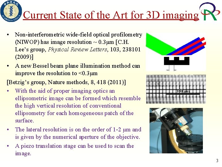
Current State of the Art for 3 D imaging • Non-interferometric wide-field optical profilometry (NIWOP) has image resolution ~ 0. 3μm [C. H. Lee’s group, Physical Review Letters, 103, 238101 (2009)] • A new Bessel beam plane illumination method can improve the resolution to <0. 3μm [Betzig’s group, Nature methods, 8, 418 (2011)] • With the aid of proper imaging optics an ellipsometric image can be formed which resemble the high vertical resolution of conventional ellipsometry for each homogeneous patch of the surface. • The lateral resolution is on the order of 1 -2 μm and is given by the numerical aperture of the objective. • A piezo translation stage can be used to scan the image. 3

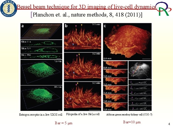
Bessel beam technique for 3 D imaging of live-cell dynamics [Planchon et. al. , nature methods, 8, 418 (2011)] Estrogen receptor in a live U 2 OS cell Filopodia of a live He. La cell Bar = 5 μm African green monkey kidney cell (COS-7) Bar=10 μm 4

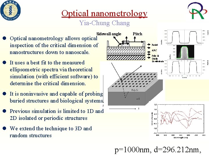
Optical Nanometrology Optical nanometrology allows optical inspection of the geometry of nanostructures down to 10 nm scale. It uses a best fit to the measured ellipsometric spectra via theoretical simulation (with efficient software) to determine the critical dimension. If done correctly, one can reconstruct images of nm resolution by using an optical instrument (with wavelengths 100 nm-1000 nm). It is noninvasive and capable of probing buried structures and biological systems 5

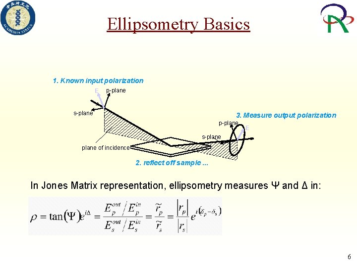
Ellipsometry Basics 1. Known input polarization E p-plane s-plane 3. Measure output polarization p-plane E s-plane of incidence 2. reflect off sample. . . In Jones Matrix representation, ellipsometry measures Ψ and Δ in: 6

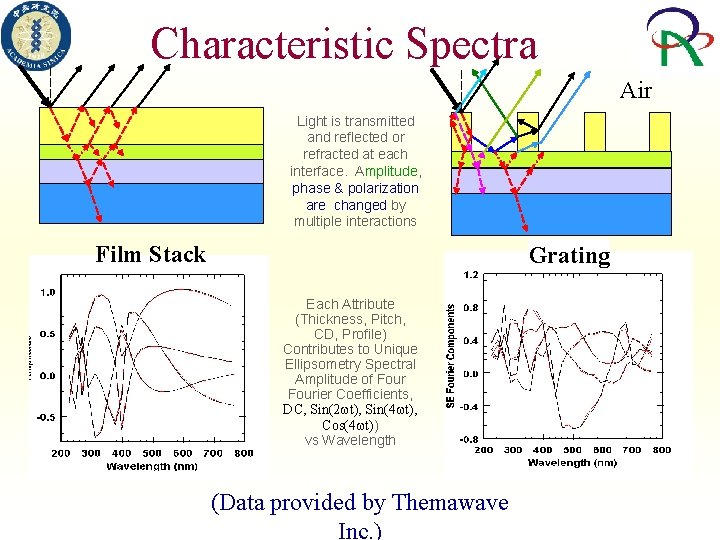
Characteristic Spectra Air Light is transmitted and reflected or refracted at each interface. Amplitude, phase & polarization are changed by multiple interactions Film Stack Grating Each Attribute (Thickness, Pitch, CD, Profile) Contributes to Unique Ellipsometry Spectral Amplitude of Fourier Coefficients, DC, Sin(2 t), Sin(4 t), Cos(4 t)) vs Wavelength (Data provided by Themawave Inc. ) Film Stack

Rigorous Coupled-Wave Analysis • Most used method for rigorous analysis of optical diffraction by periodic gratings. • For multilayer system with definite periodicity • EM fields in each layer are expanded in terms of a finite number (N) of plane waves • The coefficients are dertermined by matching boundary conditions at all interfaces. • The method is accurate (as long as enough plane waves are used) by not necessarily efficient (scale like N 3) 8

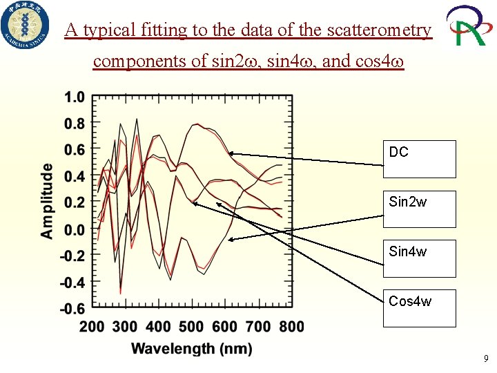
A typical fitting to the data of the scatterometry components of sin 2 , sin 4 , and cos 4 DC Sin 2 w Sin 4 w Cos 4 w 9

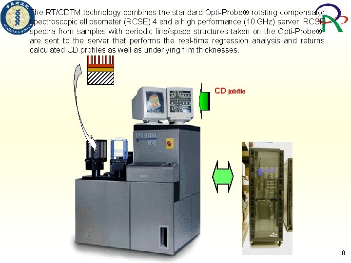
The RT/CDTM technology combines the standard Opti-Probe rotating compensator spectroscopic ellipsometer (RCSE) 4 and a high performance (10 GHz) server. RCSE spectra from samples with periodic line/space structures taken on the Opti-Probe are sent to the server that performs the real-time regression analysis and returns calculated CD profiles as well as underlying film thicknesses. CD jobfile 10

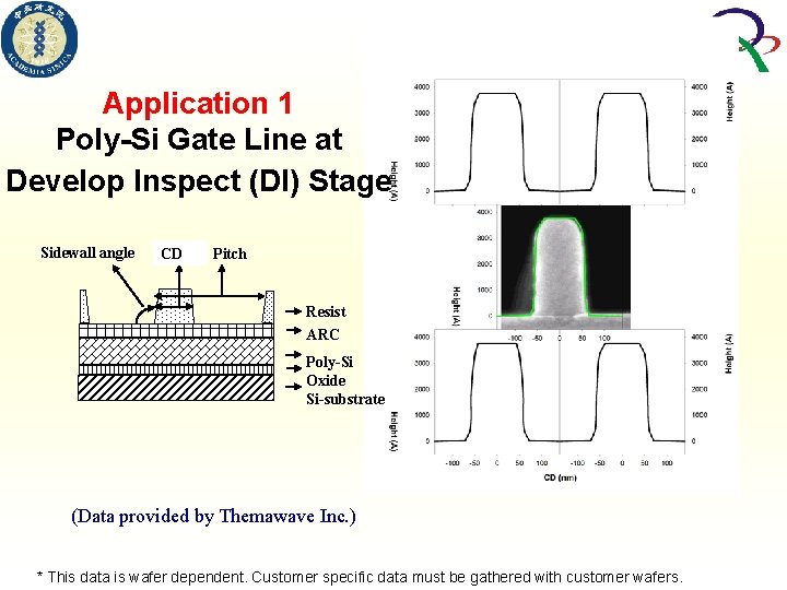
Application 1 Poly-Si Gate Line at Develop Inspect (DI) Stage Sidewall angle CD Pitch Resist ARC Poly-Si Oxide Si-substrate (Data provided by Themawave Inc. ) * This data is wafer dependent. Customer specific data must be gathered with customer wafers.

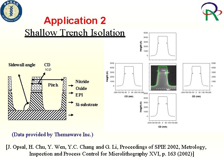
Application 2 Shallow Trench Isolation Sidewall angle CD 1 CD Pitch Nitride Oxide EPI Si-substrate (Data provided by Themawave Inc. ) [J. Opsal, H. Chu, Y. Wen, Y. C. Chang and G. Li, Proceedings of SPIE 2002, Metrology, Inspection and Process Control for Microlithography XVI, p. 163 (2002)]

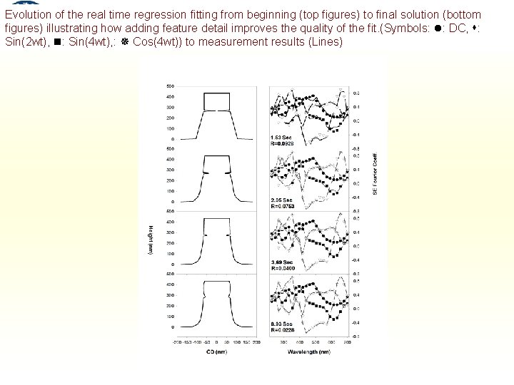
Evolution of the real time regression fitting from beginning (top figures) to final solution (bottom figures) illustrating how adding feature detail improves the quality of the fit. (Symbols: : DC, : Sin(2 wt), : Sin(4 wt), : Cos(4 wt)) to measurement results (Lines)

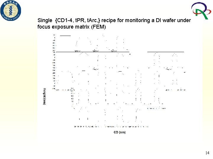
Single {CD 1 -4, t. PR, t. Arc, } recipe for monitoring a DI wafer under focus exposure matrix (FEM) 14

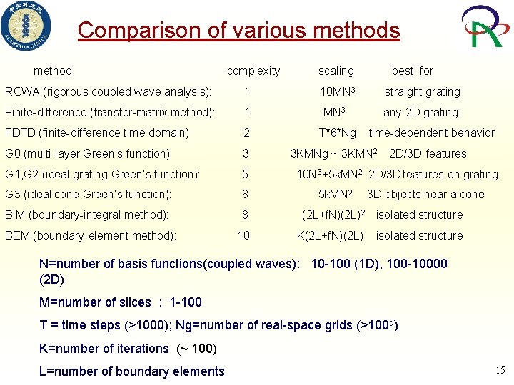
Comparison of various method complexity scaling best for RCWA (rigorous coupled wave analysis): 1 10 MN 3 straight grating Finite-difference (transfer-matrix method): 1 MN 3 any 2 D grating FDTD (finite-difference time domain) 2 T*6*Ng G 0 (multi-layer Green’s function): 3 G 1, G 2 (ideal grating Green’s function): 5 G 3 (ideal cone Green’s function): 8 BIM (boundary-integral method): 8 BEM (boundary-element method): 10 time-dependent behavior 3 KMNg ~ 3 KMN 2 2 D/3 D features 10 N 3+5 k. MN 2 2 D/3 D features on grating 5 k. MN 2 3 D objects near a cone (2 L+f. N)(2 L) 2 isolated structure K(2 L+f. N)(2 L) isolated structure N=number of basis functions(coupled waves): 10 -100 (1 D), 100 -10000 (2 D) M=number of slices : 1 -100 T = time steps (>1000); Ng=number of real-space grids (>100 d) K=number of iterations (~ 100) L=number of boundary elements 15

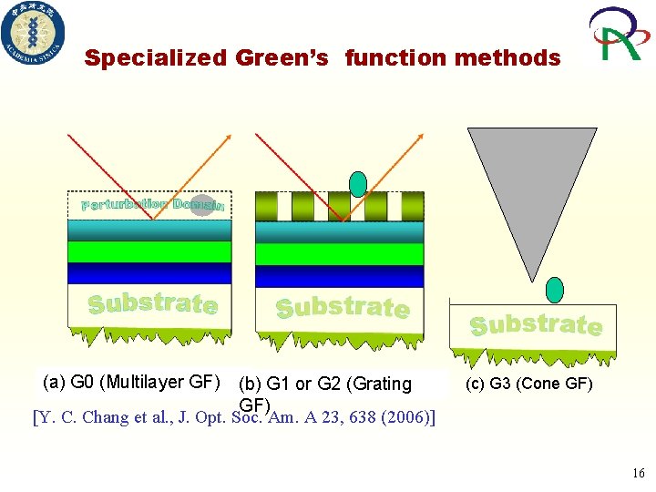
Specialized Green’s function methods (a) G 0 (Multilayer GF) (b) G 1 or G 2 (Grating GF) [Y. C. Chang et al. , J. Opt. Soc. Am. A 23, 638 (2006)] (c) G 3 (Cone GF) 16

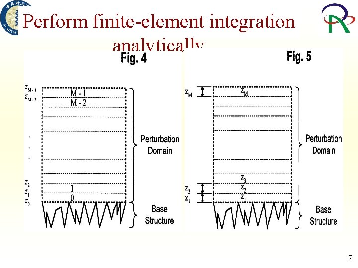
Perform finite-element integration analytically 17

18

) 19

20

21

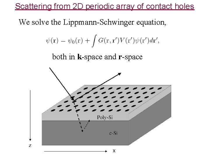
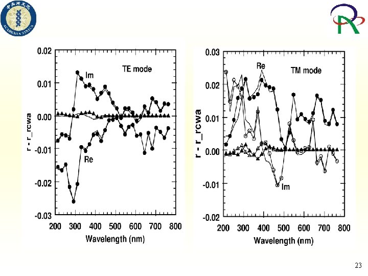
Scattering from 2 D periodic array of contact holes We solve the Lippmann-Schwinger equation, both in k-space and r-space

23

24

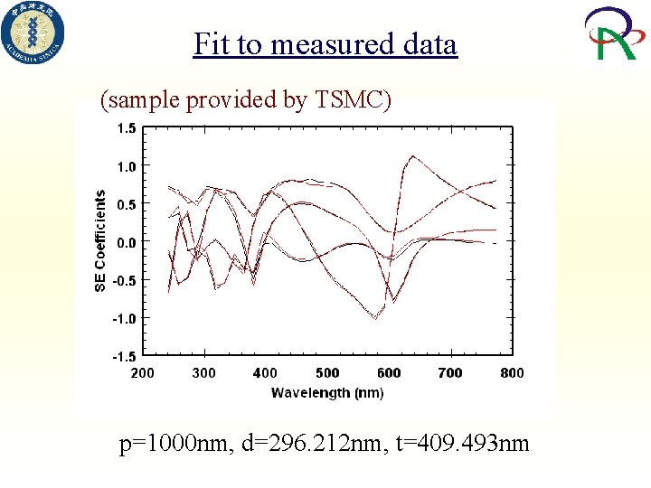
Fit to measured data (sample provided by TSMC) p=1000 nm, d=296. 212 nm, t=409. 493 nm

New efficient Method … We developed a Green function approach which can model nanoparticle clusters embedded in a random distribution of nanoparticles … • substrate

Ellipsometry measurements of Au nanoparticles on a substrate Motivation Au nanoparticles of definite size can be obtained commercially. They can be placed on insulating substrate and serve as a mask for making nanostructures. It is desirable to have a characterizing tool that can detect the density and uniformalty of the distribution of Au nanoparticles on a substrate. Ellipsometry is an optical characterizing tool that is noninvasivce, can penetrate deep into the material, and can be used in-situ during growth. Here we try to explore the capability of elliposmetry for characterizing nanoscale structures on surface or in burried interface. 27

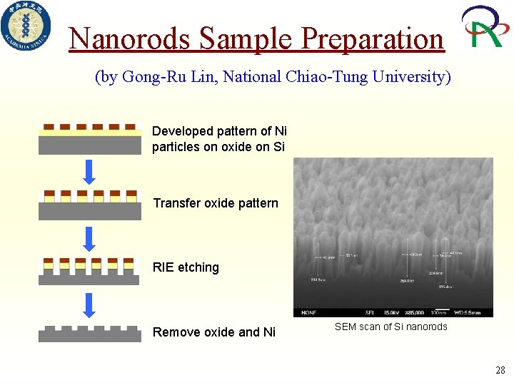
Nanorods Sample Preparation (by Gong-Ru Lin, National Chiao-Tung University) Developed pattern of Ni particles on oxide on Si Transfer oxide pattern RIE etching Remove oxide and Ni SEM scan of Si nanorods 28

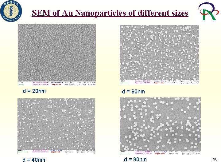
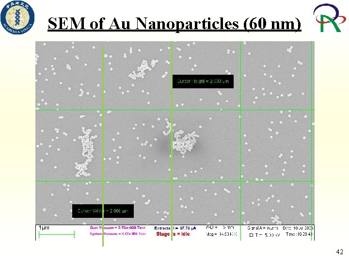
SEM of Au Nanoparticles of different sizes d = 20 nm d = 40 nm d = 60 nm d = 80 nm 29

VUV-VASE Specifications (J. A. Woollam Co. ) þ Rotating analyzer ellipsometer configuration (RAE) with the addition of Auto. Retarder þ Dry nitrogen purge to eliminate absorption from ambient water vapor and oxygen þ Spectral range: 140 nm ~ 1700 nm þ Angle of incidence: 10° ~ 90° 30

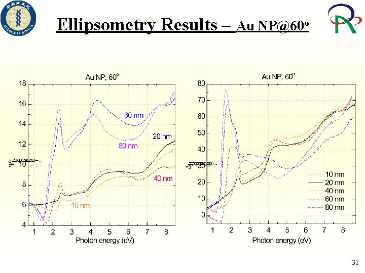
Ellipsometry Results – Au NP@60 o 31

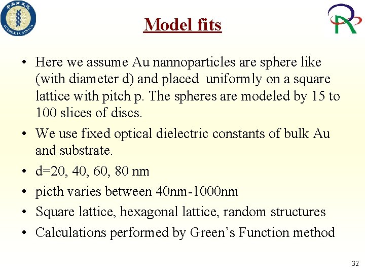
Model fits • Here we assume Au nannoparticles are sphere like (with diameter d) and placed uniformly on a square lattice with pitch p. The spheres are modeled by 15 to 100 slices of discs. • We use fixed optical dielectric constants of bulk Au and substrate. • d=20, 40, 60, 80 nm • picth varies between 40 nm-1000 nm • Square lattice, hexagonal lattice, random structures • Calculations performed by Green’s Function method 32

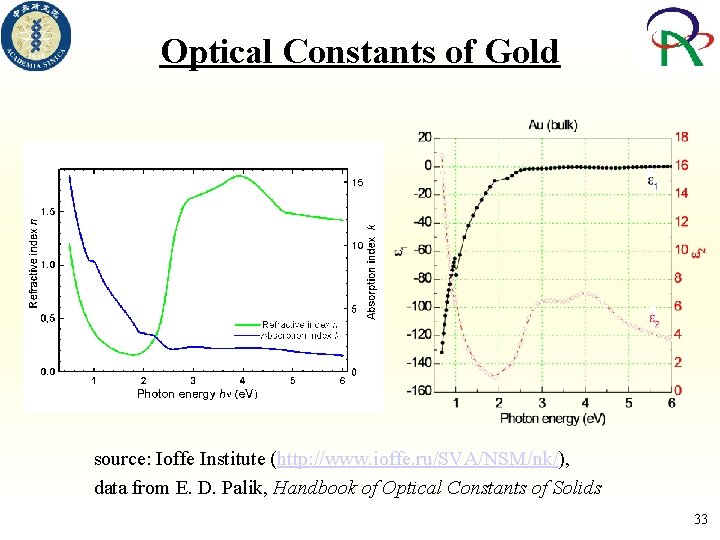
Optical Constants of Gold source: Ioffe Institute (http: //www. ioffe. ru/SVA/NSM/nk/), data from E. D. Palik, Handbook of Optical Constants of Solids 33

Effects of Disorder 34

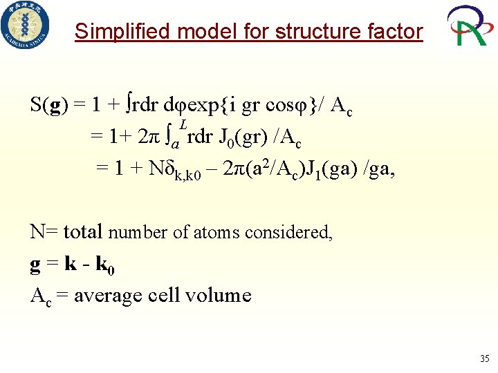
Simplified model for structure factor S(g) = 1 + ∫rdr dφexp{i gr cosφ}/ Ac L = 1+ 2π ∫a rdr J 0(gr) /Ac = 1 + Nδk, k 0 – 2π(a 2/Ac)J 1(ga) /ga, N= total number of atoms considered, g = k - k 0 Ac = average cell volume 35

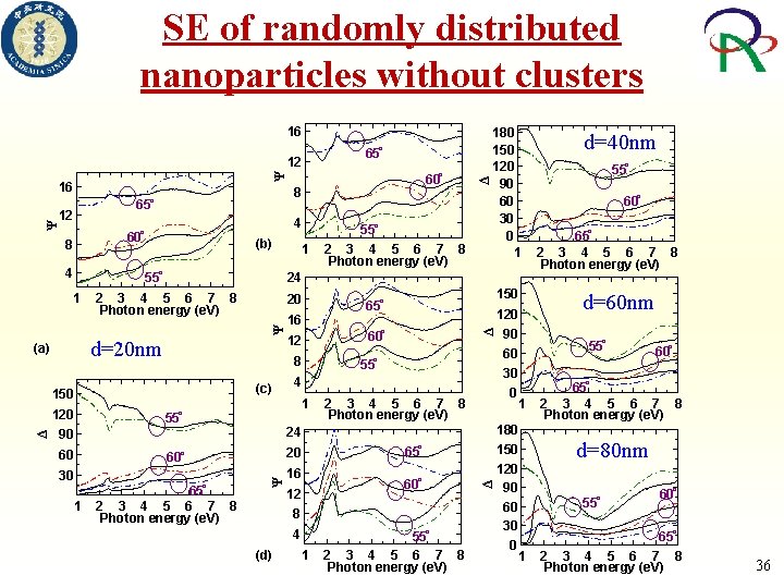
SE of randomly distributed nanoparticles without clusters 16 o 12 Ψ 16 65 4 o 60 8 4 (b) o 55 2 3 4 5 6 7 8 Photon energy (e. V) 20 d=20 nm (a) (c) 150 o 65 16 120 o 60 12 8 150 120 1 24 Ψ 1 o 55 2 3 4 5 6 7 8 Photon energy (e. V) Δ Ψ 12 60 8 o 55 1 o 0 2 3 4 5 6 7 8 Photon energy (e. V) o 1 65 2 3 4 5 6 7 8 Photon energy (e. V) 16 o 60 12 Δ 60 30 65 20 o 60 o 8 o 4 (d) 1 55 2 3 4 5 6 7 8 Photon energy (e. V) d=40 nm o 55 o 60 o 65 2 3 4 5 6 7 8 Photon energy (e. V) d=60 nm o 55 30 24 90 90 60 o 4 55 Ψ Δ o Δ 65 180 150 120 90 60 30 0 1 o 60 o 1 180 150 120 90 60 30 0 1 65 2 3 4 5 6 7 8 Photon energy (e. V) d=80 nm o o 55 60 o 65 2 3 4 5 6 7 8 Photon energy (e. V) 36

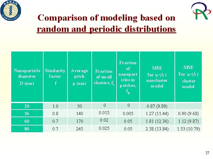
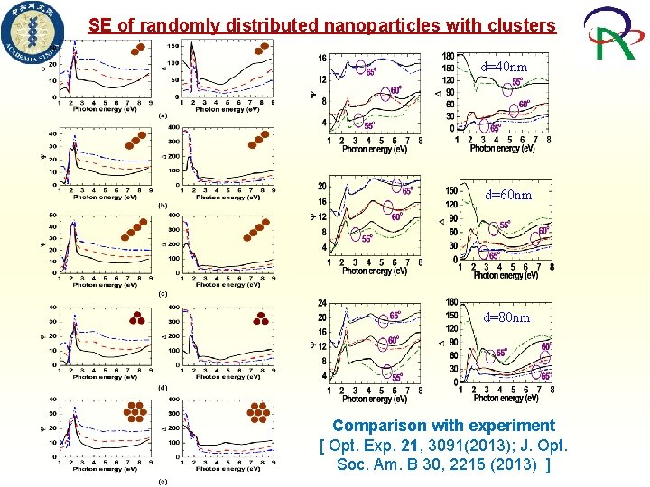
Comparison of modeling based on random and periodic distributions Nanoparticle diameter D (nm) Similarity factor f Average pitch p (nm) Fraction of small clusters, fc Fraction of nanopart icles in patches, fp 20 1. 0 50 0 0 0. 87 (9. 89) 36 0. 8 140 0. 015 0. 005 1. 27 (11. 44) 0. 90 (9. 68) 60 0. 7 170 0. 02 0. 05 1. 81 (12. 36) 1. 12 (9. 87) 80 0. 7 245 0. 025 0. 05 2. 38 (13. 84) 1. 53 (10. 79) MSE for ψ (Δ ) noncluster model MSE For ψ (Δ ) cluster model 37

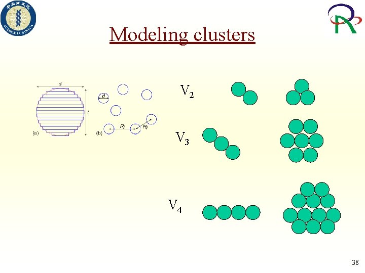
Modeling clusters V 2 V 3 V 4 38

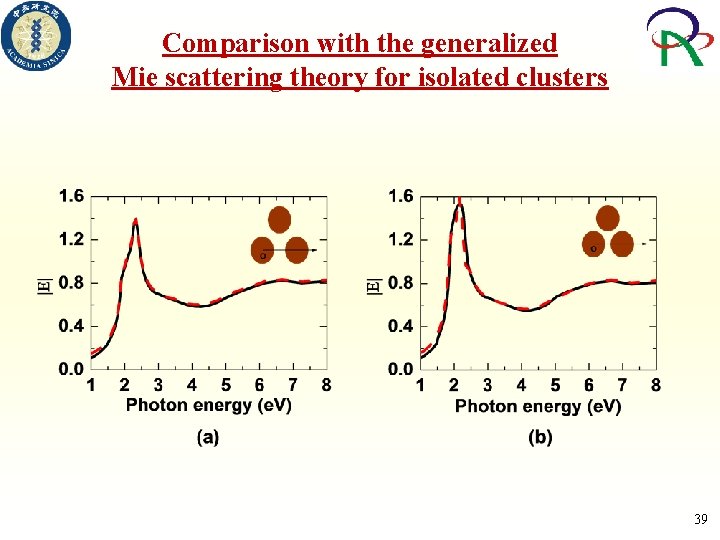
Comparison with the generalized Mie scattering theory for isolated clusters 39

SE of randomly distributed nanoparticles with clusters d=40 nm d=60 nm d=80 nm Comparison with experiment [ Opt. Exp. 21, 3091(2013); J. Opt. Soc. Am. B 30, 2215 (2013) ]

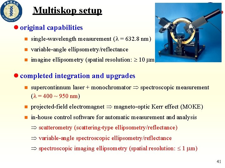
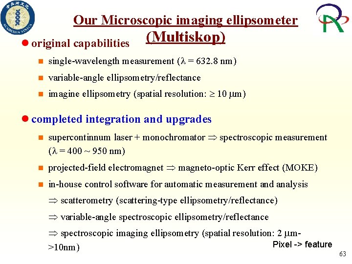
Multiskop setup original capabilities single-wavelength measurement (l = 632. 8 nm) variable-angle ellipsometry/reflectance imagine ellipsometry (spatial resolution: 10 mm) completed integration and upgrades supercontinnum laser + monochromator spectroscopic measurement (l = 400 ~ 950 nm) projected-field electromagnet magneto-optic Kerr effect (MOKE) in-house control software for automatic measurement and analysis scatterometry (scattering-type ellipsometry/reflectance) variable-angle spectroscopic ellipsometry/reflectance spectroscopic imaging ellipsometry (spatial resolution: 1 mm) 41

SEM of Au Nanoparticles (60 nm) 42

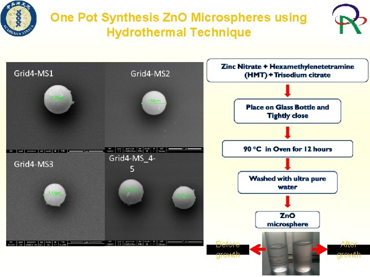
One Pot Synthesis Zn. O Microspheres using Hydrothermal Technique Before growth After growth

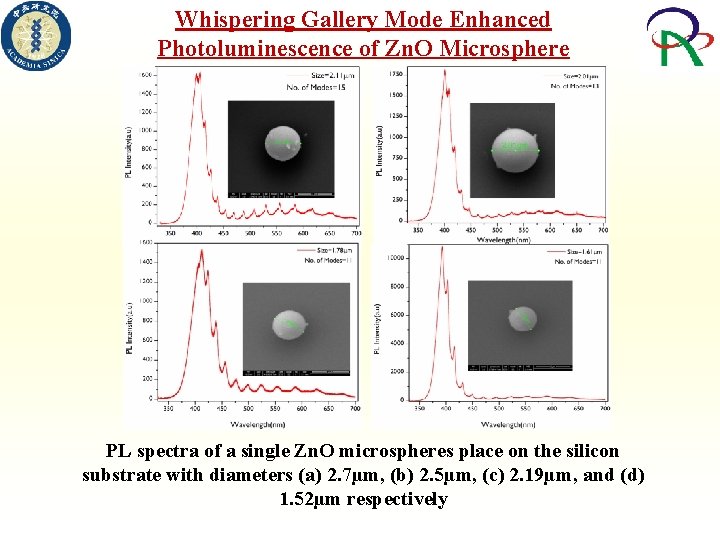
Whispering Gallery Mode Enhanced Photoluminescence of Zn. O Microsphere PL spectra of a single Zn. O microspheres place on the silicon substrate with diameters (a) 2. 7µm, (b) 2. 5µm, (c) 2. 19µm, and (d) 1. 52µm respectively

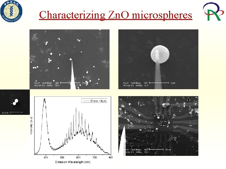
Characterizing Zn. O microspheres

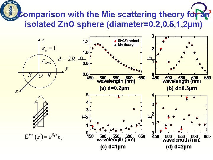
Comparison with the Mie scattering theory for an isolated Zn. O sphere (diameter=0. 2, 0. 5, 1, 2µm) (a) d=0. 2µm (b) d=0. 5µm (c) d=1µm (d) d=2µm

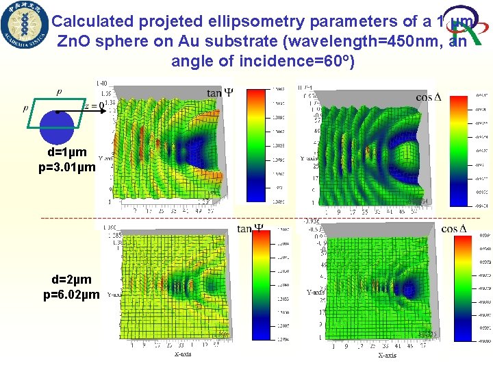
Calculated projeted ellipsometry parameters of a 1 μm Zn. O sphere on Au substrate (wavelength=450 nm, an angle of incidence=60 o) d=1µm p=3. 01µm d=2µm p=6. 02µm

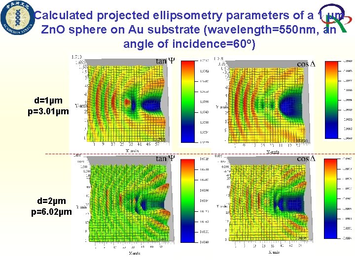
Calculated projected ellipsometry parameters of a 1 μm Zn. O sphere on Au substrate (wavelength=550 nm, an angle of incidence=60 o) d=1µm p=3. 01µm d=2µm p=6. 02µm

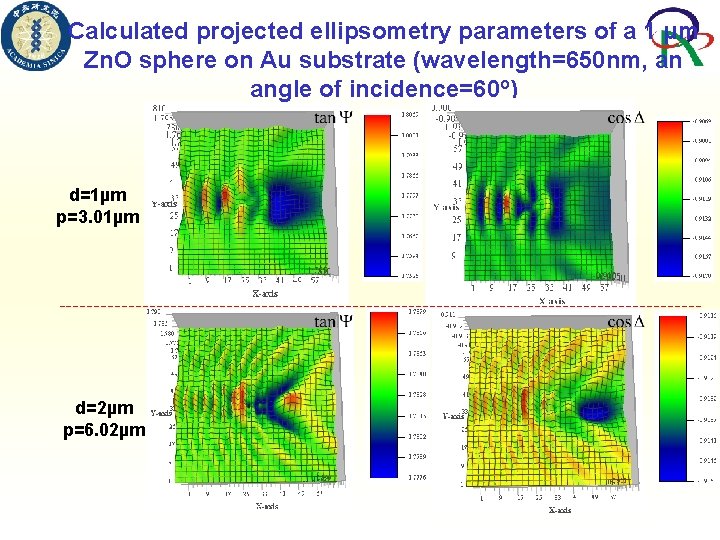
Calculated projected ellipsometry parameters of a 1 μm Zn. O sphere on Au substrate (wavelength=650 nm, an angle of incidence=60 o) d=1µm p=3. 01µm d=2µm p=6. 02µm

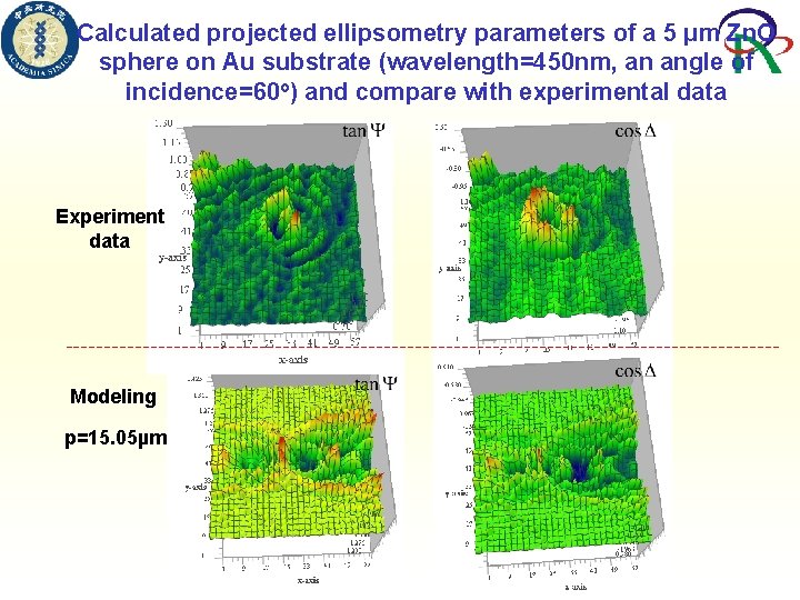
Calculated projected ellipsometry parameters of a 5 μm Zn. O sphere on Au substrate (wavelength=450 nm, an angle of incidence=60 o) and compare with experimental data Experiment data Modeling p=15. 05µm

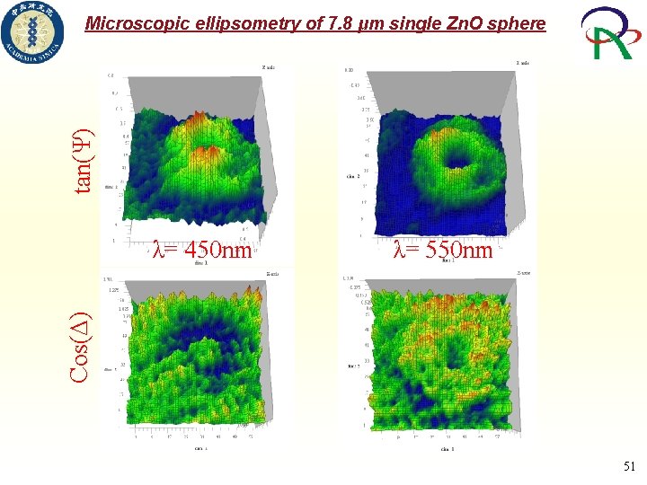
tan(Ψ) Microscopic ellipsometry of 7. 8 μm single Zn. O sphere Cos(Δ) λ= 450 nm λ= 550 nm 51

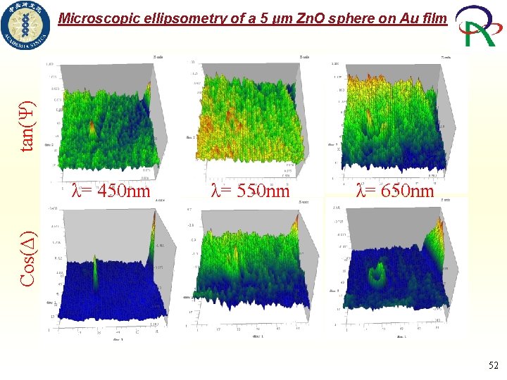
tan(Ψ) Microscopic ellipsometry of a 5 μm Zn. O sphere on Au film Cos(Δ) λ= 450 nm λ= 550 nm λ= 650 nm 52

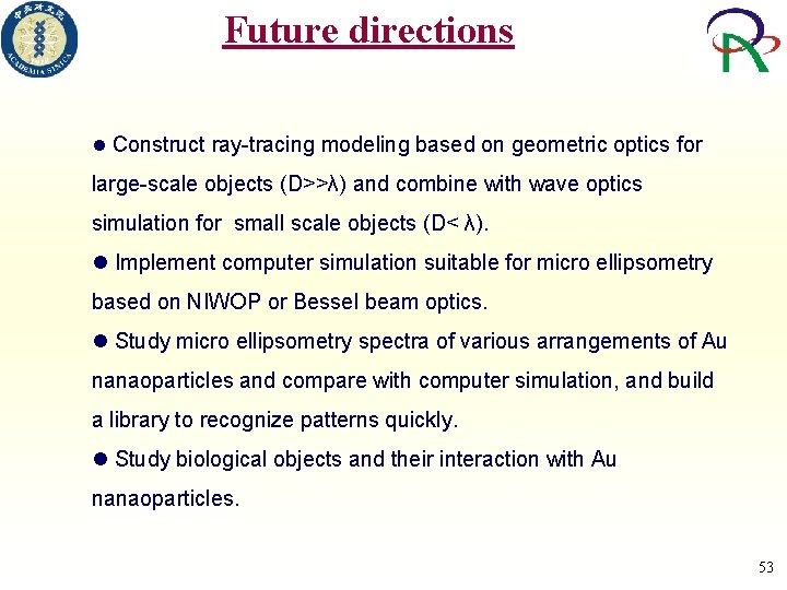
Future directions Construct ray-tracing modeling based on geometric optics for large-scale objects (D>>λ) and combine with wave optics simulation for small scale objects (D< λ). Implement computer simulation suitable for micro ellipsometry based on NIWOP or Bessel beam optics. Study micro ellipsometry spectra of various arrangements of Au nanaoparticles and compare with computer simulation, and build a library to recognize patterns quickly. Study biological objects and their interaction with Au nanaoparticles. 53

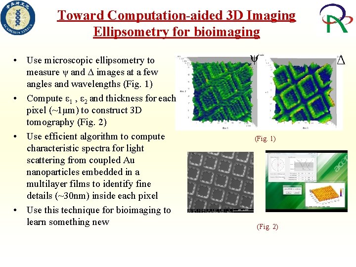
Toward Computation-aided 3 D Imaging Ellipsometry for bioimaging • Use microscopic ellipsometry to measure ψ and Δ images at a few angles and wavelengths (Fig. 1) • Compute ε 1 , ε 2 and thickness for each pixel (~1μm) to construct 3 D tomography (Fig. 2) • Use efficient algorithm to compute characteristic spectra for light scattering from coupled Au nanoparticles embedded in a multilayer films to identify fine details (~30 nm) inside each pixel • Use this technique for bioimaging to learn something new ψ (Fig. 1) (Fig. 2) Δ

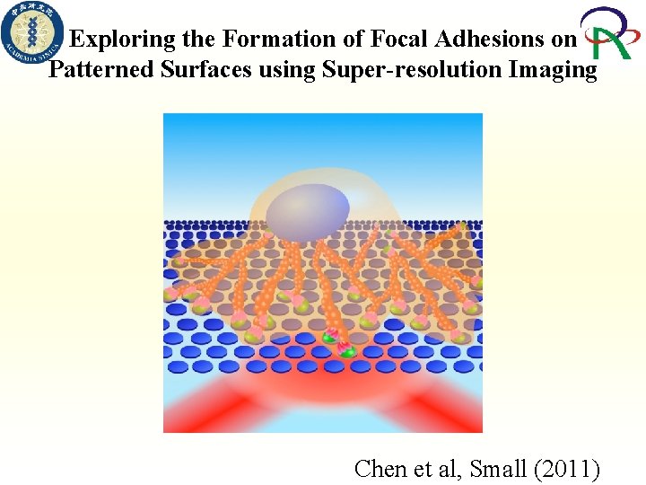
Exploring the Formation of Focal Adhesions on Patterned Surfaces using Super-resolution Imaging Chen et al, Small (2011)

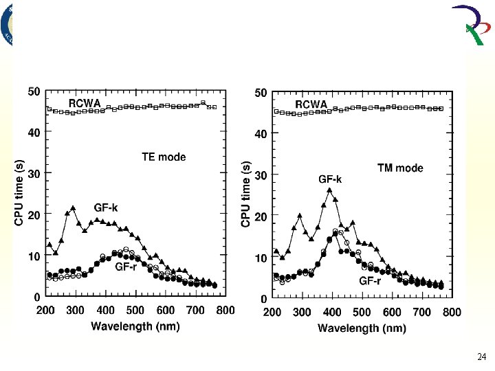
Summary Samples with different sizes of Gold nanoparticles immobilized on a glass substrate are investigated by variable-angle spectroscopic ellipsometry (VASE) in the UV to near IR region. Both the Green’s function method and rigorous coupled-wave analysis (RCWA) were used to model the ellipsometric spectra GF method is 10 – 100 times more efficient than RCWA in most cases for lattice model calculation. For random scattering problem, only GF method is used, and it is faster by another order of magnitude. Our model calculations show reasonable agreement with the ellipsometric measurements. This demonstrates that the spectroscopic ellipsometry (SE) could be a useful tool to provide information about the size and distribution of nanoparticles deposited on insulating substrate. The technique can be extended to 3 D imaging SE to inspect 56

57

58

59

60

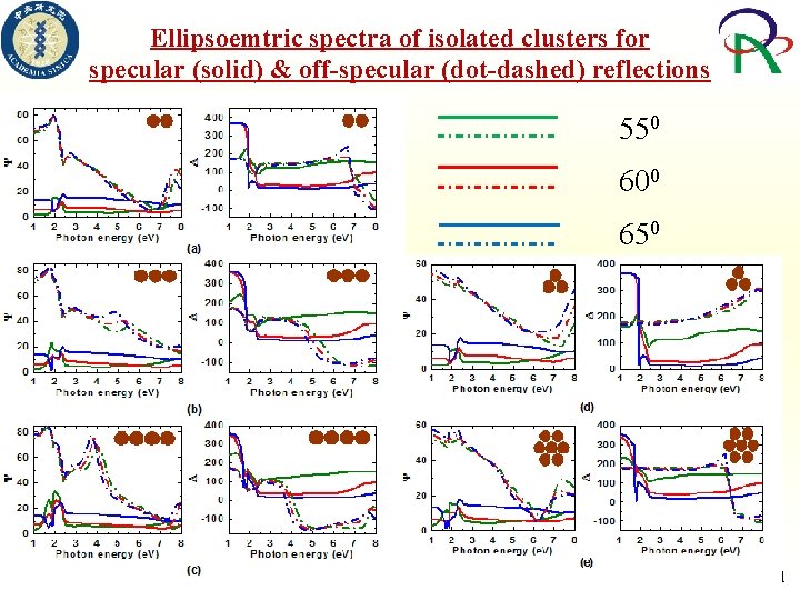
Ellipsoemtric spectra of isolated clusters for specular (solid) & off-specular (dot-dashed) reflections 550 600 650 61

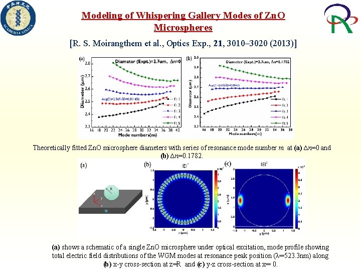
Modeling of Whispering Gallery Modes of Zn. O Microspheres [R. S. Moirangthem et al. , Optics Exp. , 21, 3010– 3020 (2013)] Theoretically fitted Zn. O microsphere diameters with series of resonance mode number m at (a) ∆n=0 and (b) ∆n=0. 1782. (a) shows a schematic of a single Zn. O microsphere under optical excitation, mode profile showing total electric field distributions of the WGM modes at resonance peak position (λ═ 523. 3 nm) along (b) x-y cross-section at z=R and (c) y-z cross-section at x═ 0.

Our Microscopic imaging ellipsometer original capabilities (Multiskop) single-wavelength measurement (l = 632. 8 nm) variable-angle ellipsometry/reflectance imagine ellipsometry (spatial resolution: 10 mm) completed integration and upgrades supercontinnum laser + monochromator spectroscopic measurement (l = 400 ~ 950 nm) projected-field electromagnet magneto-optic Kerr effect (MOKE) in-house control software for automatic measurement and analysis scatterometry (scattering-type ellipsometry/reflectance) variable-angle spectroscopic ellipsometry/reflectance spectroscopic imaging ellipsometry (spatial resolution: 2 mm. Pixel -> feature >10 nm) 63

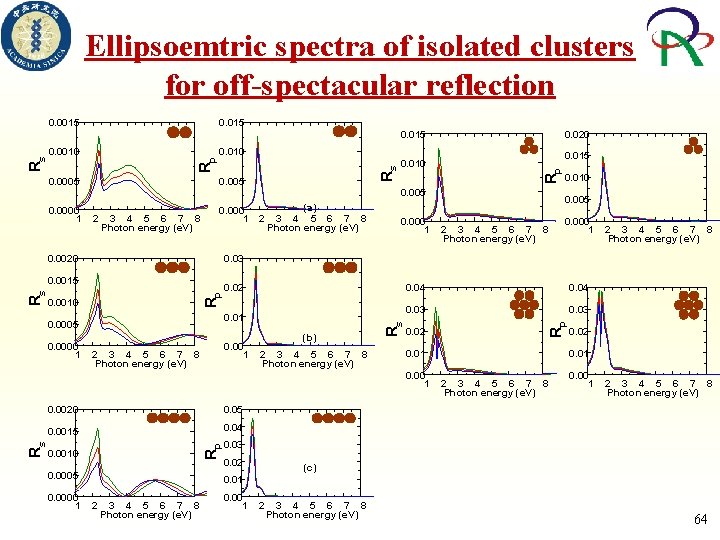
Ellipsoemtric spectra of isolated clusters for off-spectacular reflection 0. 0015 0. 005 0. 010 0. 015 Rp 0. 0005 0. 020 0. 010 Rs 0. 0010 Rp Rs 0. 015 0. 005 2 3 4 5 6 7 8 Photon energy (e. V) 0. 000 1 Rp Rs 0. 0010 0. 02 0. 01 0. 0005 0. 00 1 2 3 4 5 6 7 8 Photon energy (e. V) 0. 0020 0. 05 0. 0015 0. 04 Rp Rs 0. 000 1 (b) 2 3 4 5 6 7 8 Photon energy (e. V) 0. 04 0. 03 0. 02 0. 01 0. 0010 0. 0005 0. 0000 1 2 3 4 5 6 7 8 Photon energy (e. V) 0. 03 0. 0015 0. 0000 1 0. 005 Rp 0. 0020 (a) 2 3 4 5 6 7 8 Photon energy (e. V) Rs 0. 0000 1 0. 010 0. 02 0. 01 2 3 4 5 6 7 8 Photon energy (e. V) 0. 00 1 2 3 4 5 6 7 8 Photon energy (e. V) 0. 03 0. 02 (c) 0. 01 2 3 4 5 6 7 8 Photon energy (e. V) 0. 00 1 2 3 4 5 6 7 8 Photon energy (e. V) 64

Optical nanometrology Yia-Chung Chang Sidewall angle Optical nanometrology allows optical inspection of the critical dimension of nanostructures down to nanoscale. It uses a best fit to the measured ellipsometric spectra via theoretical simulation (with efficient software) to determine the critical dimension. Pitch Resist ARC Poly-Si Oxide Si-substrate It is noninvasive and capable of probing buried structures and biological systems Previous simulation is limited to 1 D and 2 D isolated or periodic structures We extend the technique to 3 D and random structures p=1000 nm, d=296. 212 nm,