DMT 2313 Electronic II Lecture VI Power Amplifiers
- Slides: 29

DMT 231/3 Electronic II Lecture VI Power Amplifiers Class A & Class AB

Class A Power Amplifier Large-signal amplifiers with the objective of providing power (rather than voltage) to a load.

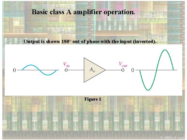
Basic class A amplifier operation. Output is shown 180° out of phase with the input (inverted). Figure 1

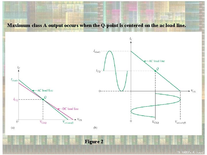
Maximum class A output occurs when the Q-point is centered on the ac load line. Figure 2

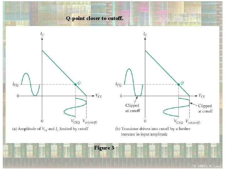
Q-point closer to cutoff. Figure 3

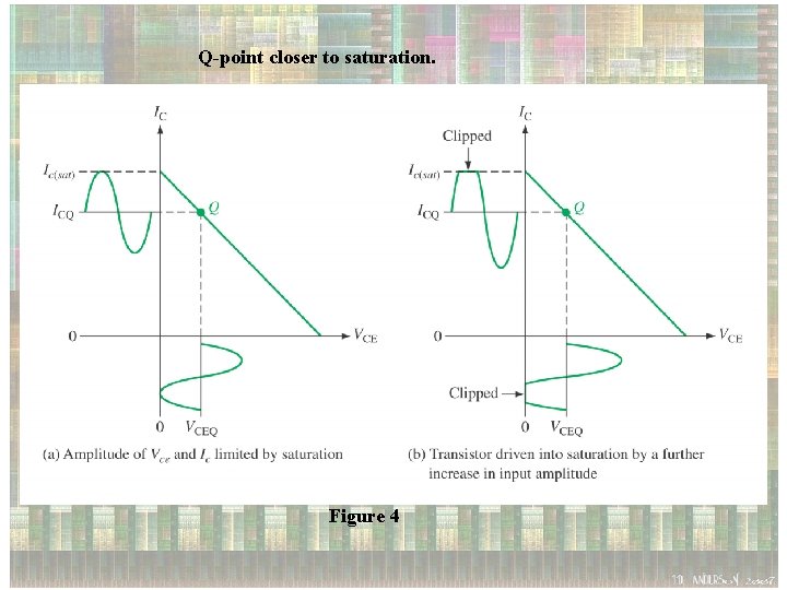
Q-point closer to saturation. Figure 4

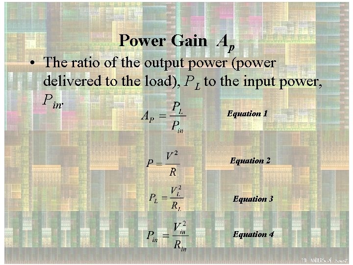
Power Gain Ap • The ratio of the output power (power delivered to the load), PL to the input power, Pin. Equation 1 Equation 2 Equation 3 Equation 4

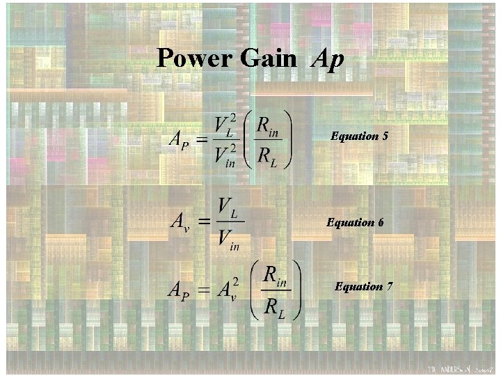
Power Gain Ap Equation 5 Equation 6 Equation 7

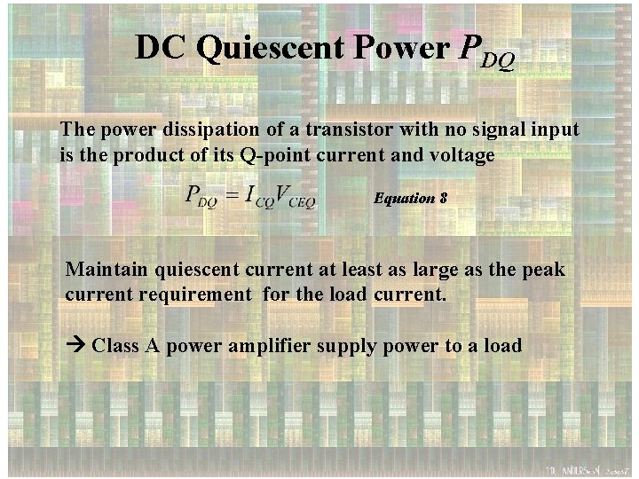
DC Quiescent Power PDQ The power dissipation of a transistor with no signal input is the product of its Q-point current and voltage Equation 8 Maintain quiescent current at least as large as the peak current requirement for the load current. Class A power amplifier supply power to a load

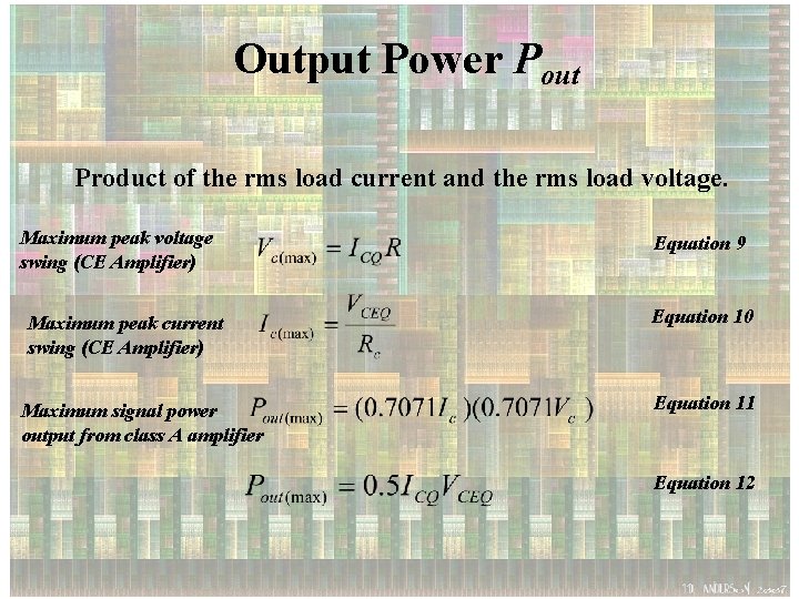
Output Power Pout Product of the rms load current and the rms load voltage. Maximum peak voltage swing (CE Amplifier) Maximum peak current swing (CE Amplifier) Maximum signal power output from class A amplifier Equation 9 Equation 10 Equation 11 Equation 12

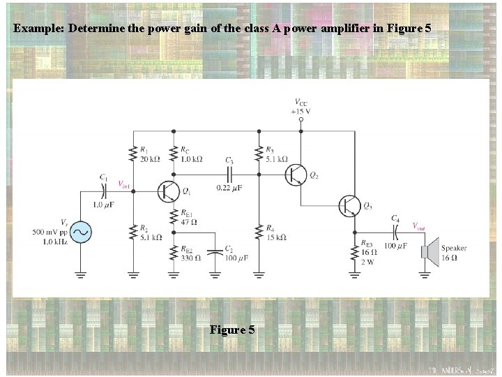
Example: Determine the power gain of the class A power amplifier in Figure 5

Class B & AB Push-Pull Power Amplifier when an amplifier is biased at cutoff so that it operates in the linear region for 180 degree of the input cycle and is in cutoff for 180 degree.

Class B & AB Push-Pull Power Amplifier MORE EFFICIENT than Class A but MORE DIFFICULT to implement the circuit in order to get linear reproduction of the input waveform. Push-pull: common type of class B or class AB amplifier circuit in which 2 transistors are used on alternating half-cycles to reproduce the input waveform at the output.

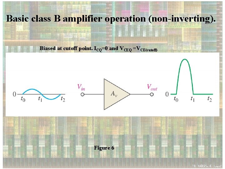
Basic class B amplifier operation (non-inverting). Biased at cutoff point. ICQ=0 and VCEQ =VCE(cutoff) Figure 6

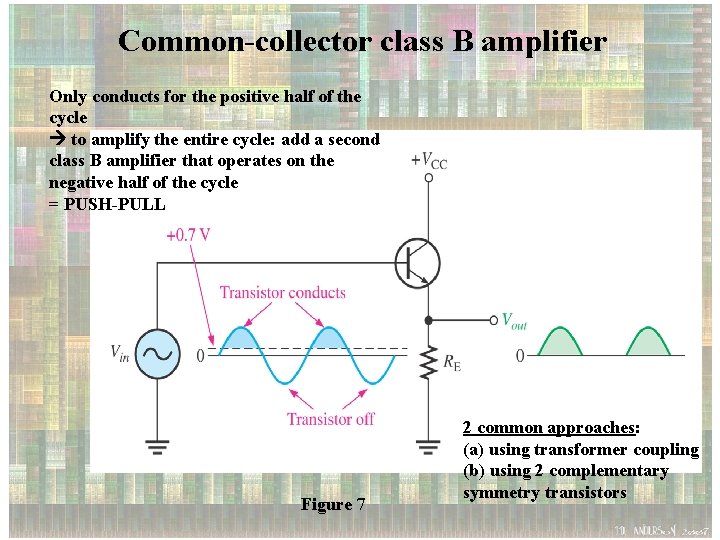
Common-collector class B amplifier Only conducts for the positive half of the cycle to amplify the entire cycle: add a second class B amplifier that operates on the negative half of the cycle = PUSH-PULL Figure 7 2 common approaches: (a) using transformer coupling (b) using 2 complementary symmetry transistors

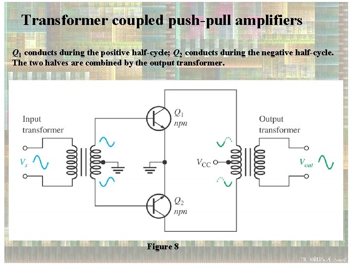
Transformer coupled push-pull amplifiers Q 1 conducts during the positive half-cycle; Q 2 conducts during the negative half-cycle. The two halves are combined by the output transformer. Figure 8

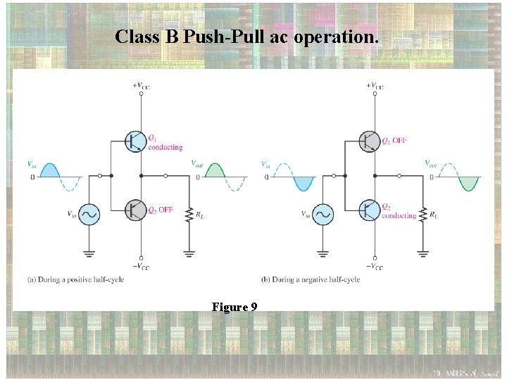
Class B Push-Pull ac operation. Figure 9

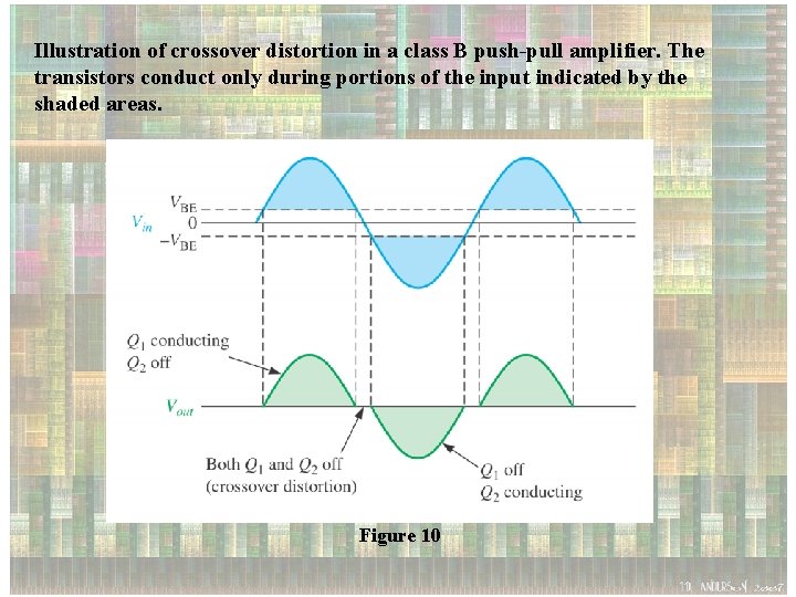
Illustration of crossover distortion in a class B push-pull amplifier. The transistors conduct only during portions of the input indicated by the shaded areas. Figure 10

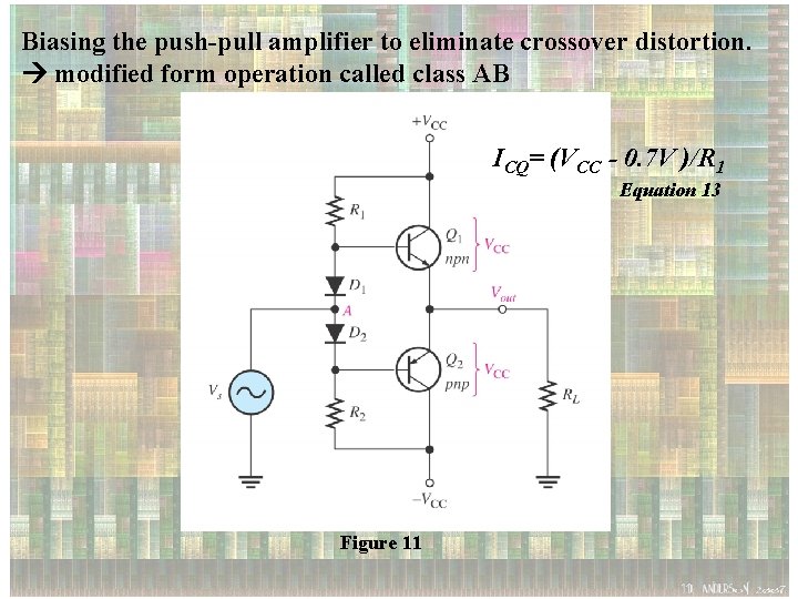
Biasing the push-pull amplifier to eliminate crossover distortion. modified form operation called class AB ICQ= (VCC - 0. 7 V )/R 1 Equation 13 Figure 11

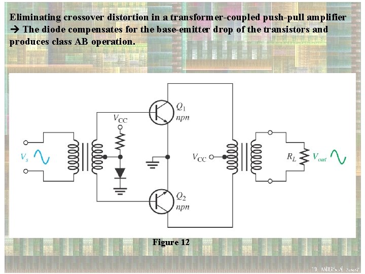
Eliminating crossover distortion in a transformer-coupled push-pull amplifier The diode compensates for the base-emitter drop of the transistors and produces class AB operation. Figure 12

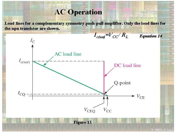
AC Operation Load lines for a complementary symmetry push-pull amplifier. Only the load lines for the npn transistor are shown. Ic(sat)=VCC / RL Figure 13 Equation 14

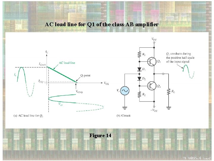
AC load line for Q 1 of the class AB amplifier Figure 14

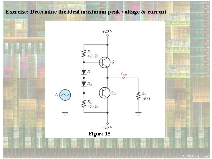
Exercise: Determine the ideal maximum peak voltage & current Figure 15

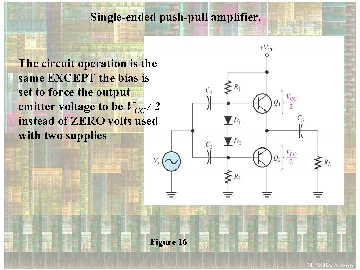
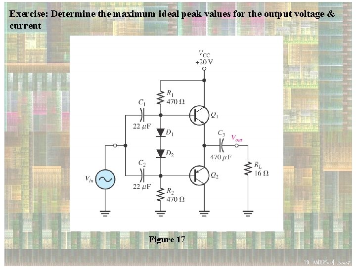
Single-ended push-pull amplifier. The circuit operation is the same EXCEPT the bias is set to force the output emitter voltage to be VCC / 2 instead of ZERO volts used with two supplies Figure 16

Exercise: Determine the maximum ideal peak values for the output voltage & current Figure 17

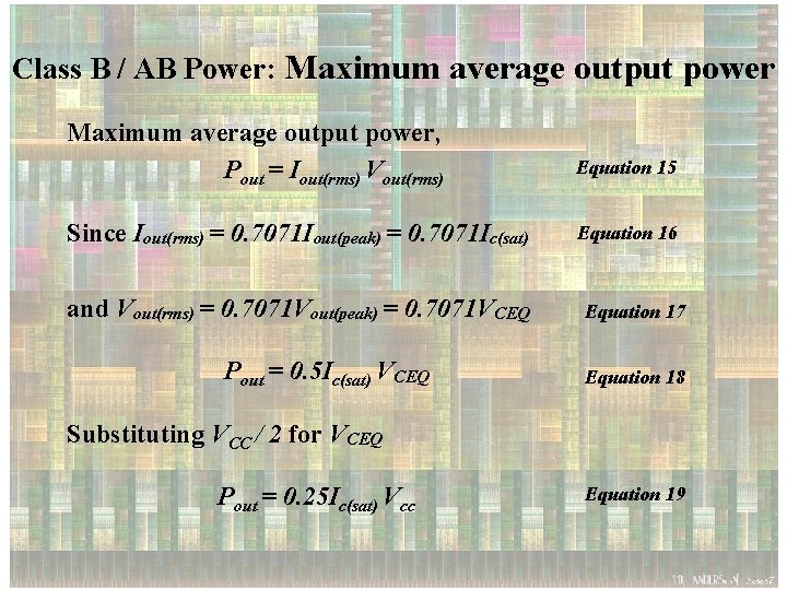
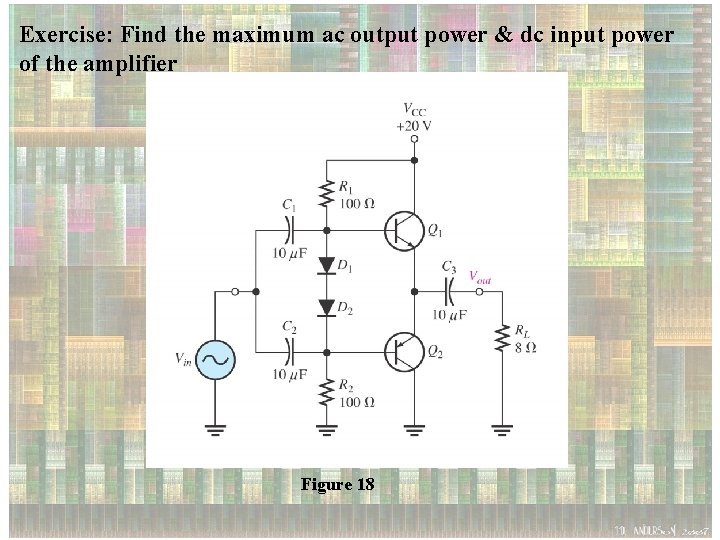
Class B / AB Power: Maximum average output power, Pout = Iout(rms) Vout(rms) Since Iout(rms) = 0. 7071 Iout(peak) = 0. 7071 Ic(sat) and Vout(rms) = 0. 7071 Vout(peak) = 0. 7071 VCEQ Pout = 0. 5 Ic(sat) VCEQ Equation 15 Equation 16 Equation 17 Equation 18 Substituting VCC / 2 for VCEQ Pout = 0. 25 Ic(sat) Vcc Equation 19

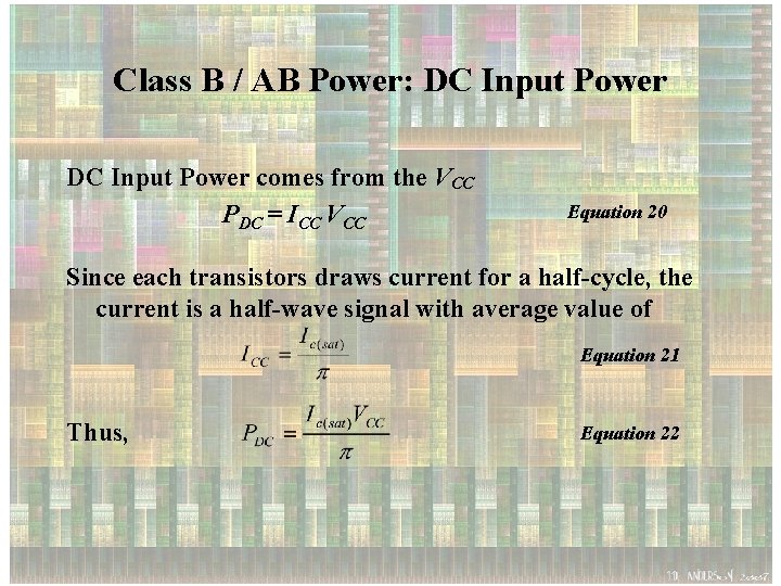
Class B / AB Power: DC Input Power comes from the VCC PDC = ICC VCC Equation 20 Since each transistors draws current for a half-cycle, the current is a half-wave signal with average value of Equation 21 Thus, Equation 22

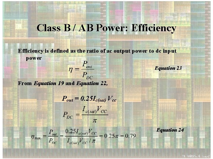
Class B / AB Power: Efficiency is defined as the ratio of ac output power to dc input power Equation 23 From Equation 19 and Equation 22, Pout = 0. 25 Ic(sat) Vcc Equation 24

Exercise: Find the maximum ac output power & dc input power of the amplifier Figure 18