Data Manipulation 672021 CheRung Lee 202167 CS 135602
![The instruction repertoire • Which instructions should be included? • For example, swapping v[k] The instruction repertoire • Which instructions should be included? • For example, swapping v[k]](https://slidetodoc.com/presentation_image_h2/5d3e150f9bdc5fcc4f1729e0ab9ef444/image-19.jpg)


![SIMD example • SISD for-loop – for(i=0; i<5; i++) A[i]=B[i]+C[i]; • SIMD expansion – SIMD example • SISD for-loop – for(i=0; i<5; i++) A[i]=B[i]+C[i]; • SIMD expansion –](https://slidetodoc.com/presentation_image_h2/5d3e150f9bdc5fcc4f1729e0ab9ef444/image-75.jpg)
- Slides: 85

Data Manipulation 6/7/2021 Che-Rung Lee 2021/6/7 CS 135602 Introduction to Information Engineering 1

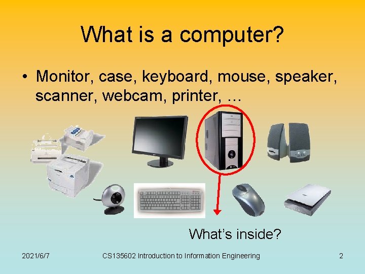
What is a computer? • Monitor, case, keyboard, mouse, speaker, scanner, webcam, printer, … What’s inside? 2021/6/7 CS 135602 Introduction to Information Engineering 2

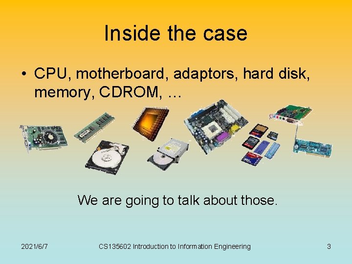
Inside the case • CPU, motherboard, adaptors, hard disk, memory, CDROM, … We are going to talk about those. 2021/6/7 CS 135602 Introduction to Information Engineering 3

Central Processing Unit (CPU) • An electronic circuit that can execute computer programs – Intel i 7 – AMD K 10 – IBM Cell – ARM Acorn – Sun SPARC • To understand CPU, we need to know what computer programs are. 2021/6/7 CS 135602 Introduction to Information Engineering 4

Outline • • • Store program concept Machine language Program execution Peripheral devices Parallel architectures 2021/6/7 CS 135602 Introduction to Information Engineering 5

Stored Program Concept "The final major step in the development of the general purpose electronic computer was the idea of a stored program. . . " Brian Randell 2021/6/7 CS 135602 Introduction to Information Engineering 6

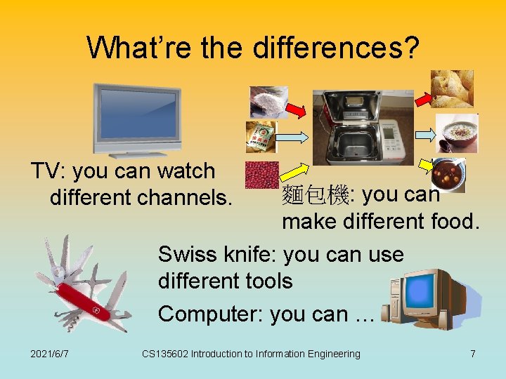
What’re the differences? TV: you can watch different channels. 麵包機: you can make different food. Swiss knife: you can use different tools Computer: you can … 2021/6/7 CS 135602 Introduction to Information Engineering 7

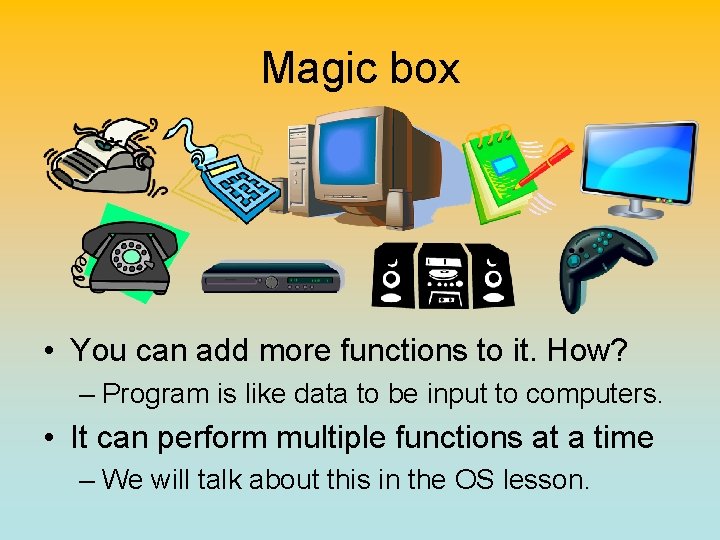
Magic box • You can add more functions to it. How? – Program is like data to be input to computers. • It can perform multiple functions at a time – We will talk about this in the OS lesson.

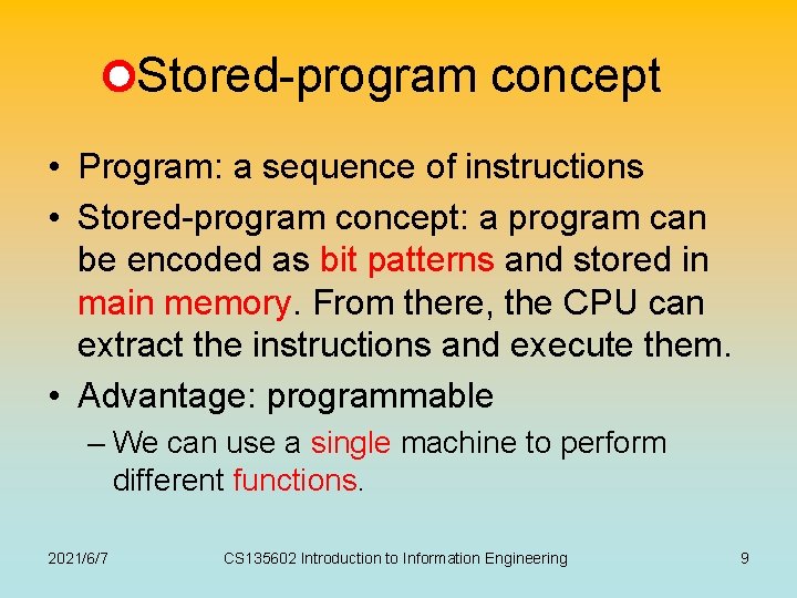
Stored-program concept • Program: a sequence of instructions • Stored-program concept: a program can be encoded as bit patterns and stored in main memory. From there, the CPU can extract the instructions and execute them. • Advantage: programmable – We can use a single machine to perform different functions. 2021/6/7 CS 135602 Introduction to Information Engineering 9

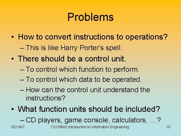
Problems • How to convert instructions to operations? – This is like Harry Porter’s spell. • There should be a control unit. – To control which function to perform. – To control which data to be operated. – How can the control unit understand the instructions? • What function units should be included? – CD players, game console, calculators, …? 2021/6/7 CS 135602 Introduction to Information Engineering 10

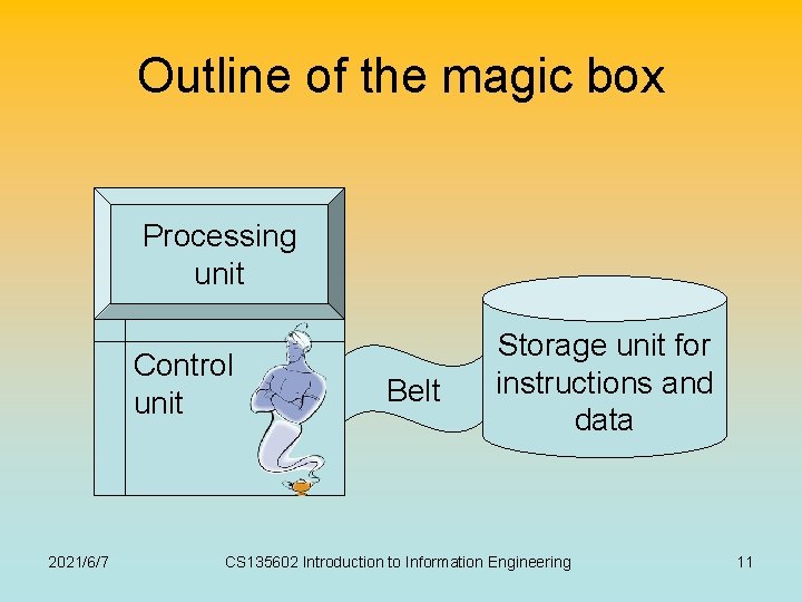
Outline of the magic box Processing unit Control unit 2021/6/7 Belt Storage unit for instructions and data CS 135602 Introduction to Information Engineering 11

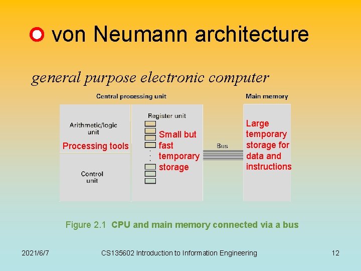
von Neumann architecture general purpose electronic computer Processing tools Small but fast temporary storage Large temporary storage for data and instructions Figure 2. 1 CPU and main memory connected via a bus 2021/6/7 CS 135602 Introduction to Information Engineering 12

Machine Language What to do + Specified information 2021/6/7 CS 135602 Introduction to Information Engineering 13

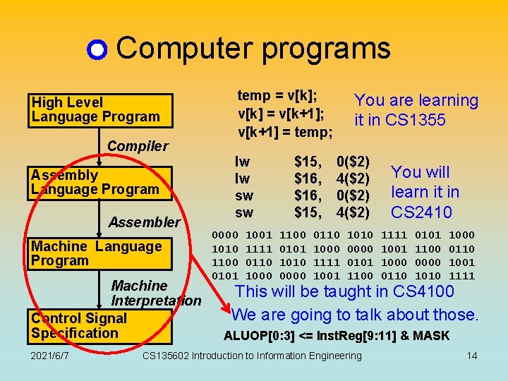
Computer programs High Level Language Program Compiler Assembly Language Program Assembler Machine Language Program Machine Interpretation Control Signal Specification 2021/6/7 temp = v[k]; v[k] = v[k+1]; v[k+1] = temp; lw lw sw sw 0000 1010 1100 0101 1001 1111 0110 1000 $15, $16, $15, 1100 0101 1010 0000 You are learning it in CS 1355 0($2) 4($2) 0110 1000 1111 1001 1010 0000 0101 1100 You will learn it in CS 2410 1111 1000 0110 0101 1100 0000 1010 1000 0110 1001 1111 This will be taught in CS 4100 We are going to talk about those. ALUOP[0: 3] <= Inst. Reg[9: 11] & MASK CS 135602 Introduction to Information Engineering 14

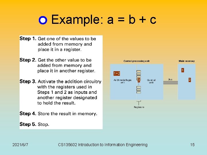
Example: a = b + c 1 1+2 3 2021/6/7 CS 135602 Introduction to Information Engineering 2 15

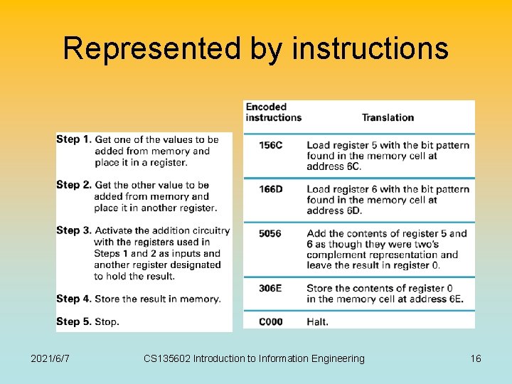
Represented by instructions 2021/6/7 CS 135602 Introduction to Information Engineering 16

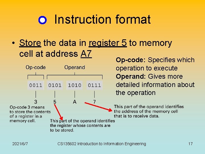
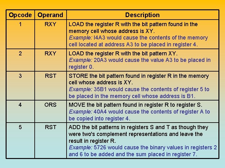
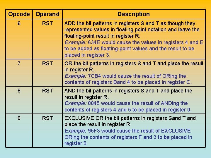
Instruction format • Store the data in register 5 to memory cell at address A 7 Op-code: Specifies which operation to execute Operand: Gives more detailed information about the operation 2021/6/7 CS 135602 Introduction to Information Engineering 17

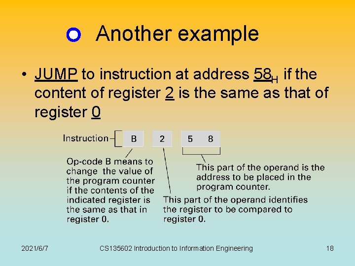
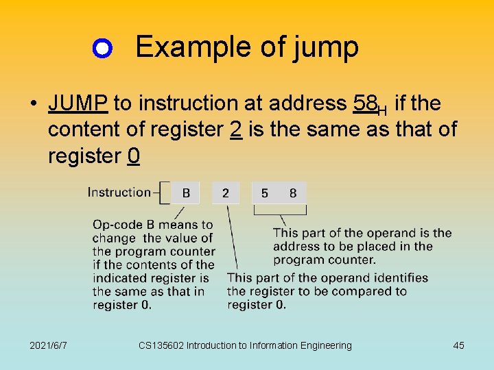
Another example • JUMP to instruction at address 58 H if the content of register 2 is the same as that of register 0 2021/6/7 CS 135602 Introduction to Information Engineering 18
![The instruction repertoire Which instructions should be included For example swapping vk The instruction repertoire • Which instructions should be included? • For example, swapping v[k]](https://slidetodoc.com/presentation_image_h2/5d3e150f9bdc5fcc4f1729e0ab9ef444/image-19.jpg)
The instruction repertoire • Which instructions should be included? • For example, swapping v[k] and v[k+1] Create a new instruction, called swp, which swaps data in two memory addresses. swp 0($2), 4($2) Complex Instruction Set Computing (CISC) 2021/6/7 Using load and store instructions lw lw sw sw $15, $16, $15, 0($2) 4($2) Reduced Instruction Set Computing (RISC) CS 135602 Introduction to Information Engineering 19

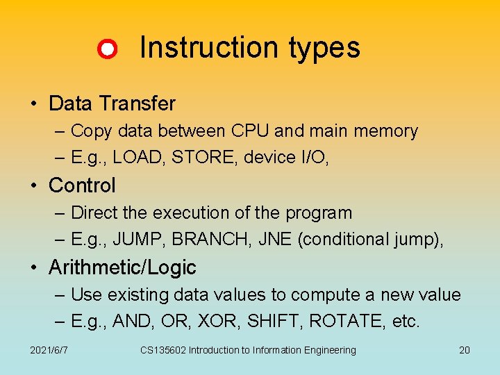
Instruction types • Data Transfer – Copy data between CPU and main memory – E. g. , LOAD, STORE, device I/O, • Control – Direct the execution of the program – E. g. , JUMP, BRANCH, JNE (conditional jump), • Arithmetic/Logic – Use existing data values to compute a new value – E. g. , AND, OR, XOR, SHIFT, ROTATE, etc. 2021/6/7 CS 135602 Introduction to Information Engineering 20

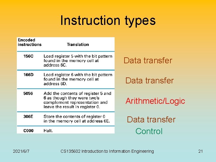
Instruction types Data transfer Arithmetic/Logic Data transfer Control 2021/6/7 CS 135602 Introduction to Information Engineering 21

Program Execution 2021/6/7 CS 135602 Introduction to Information Engineering 22

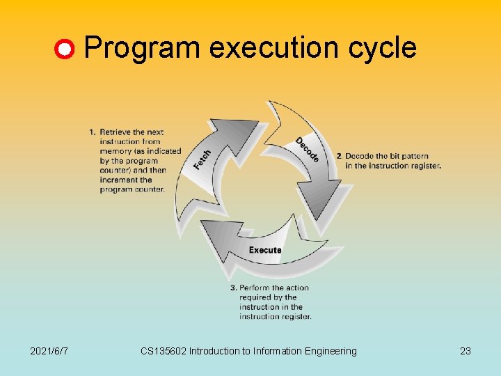
Program execution cycle 2021/6/7 CS 135602 Introduction to Information Engineering 23

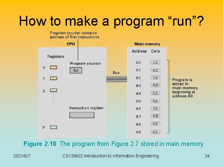
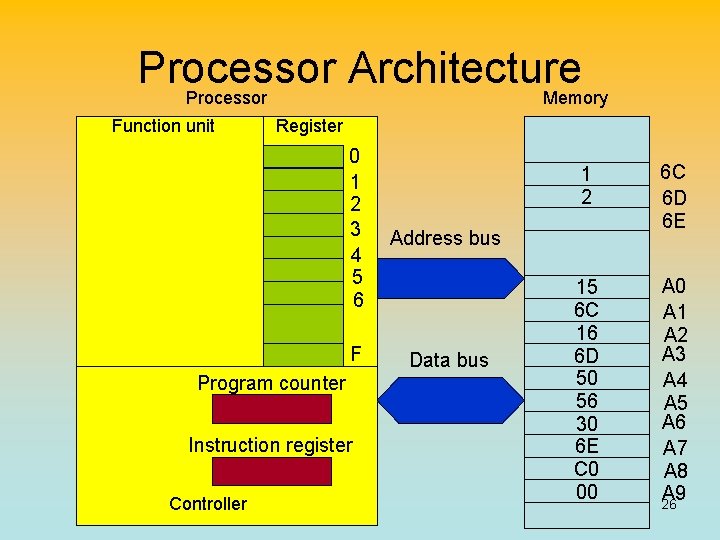
How to make a program “run”? Figure 2. 10 The program from Figure 2. 7 stored in main memory 2021/6/7 CS 135602 Introduction to Information Engineering 24

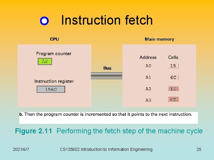
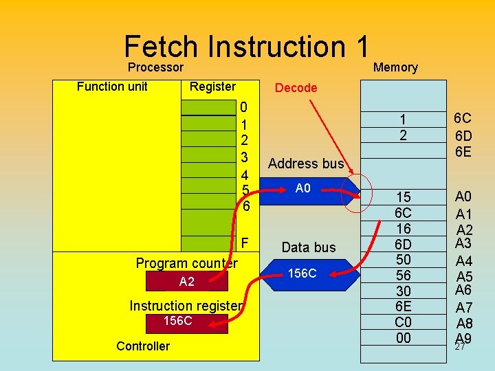
Instruction fetch Figure 2. 11 Performing the fetch step of the machine cycle 2021/6/7 CS 135602 Introduction to Information Engineering 25

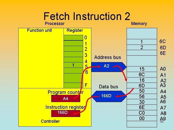
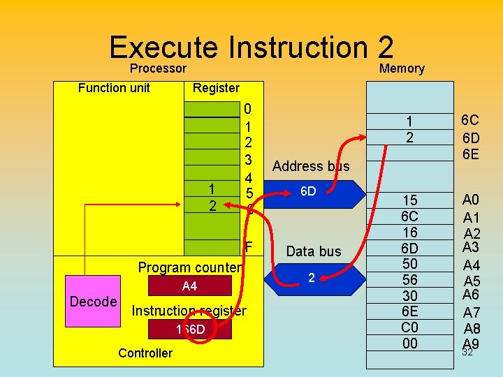
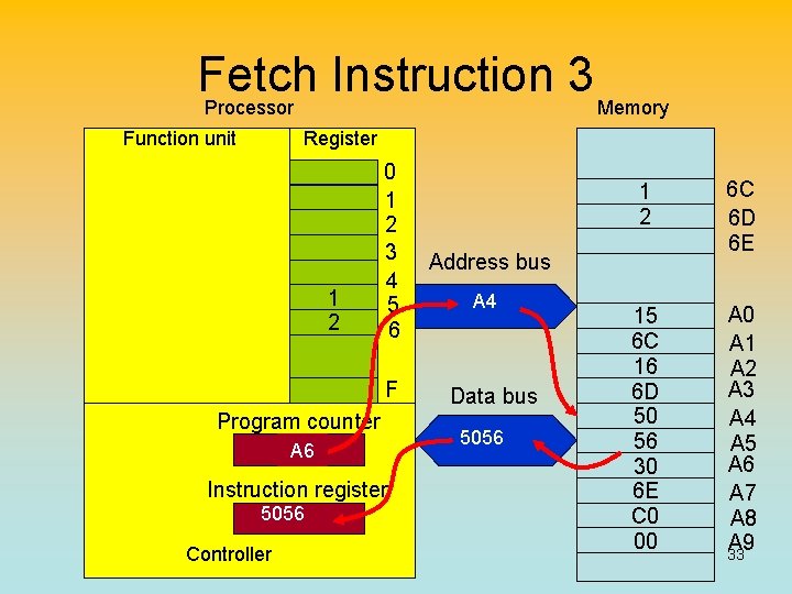
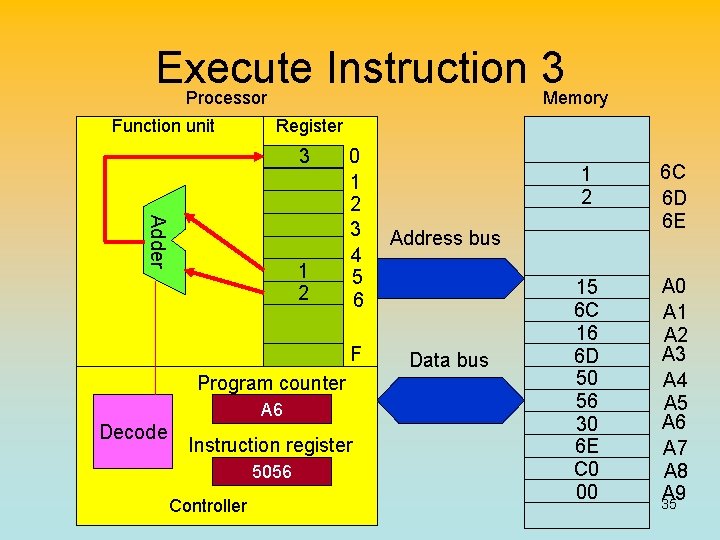
Processor Architecture Processor Memory Function unit Register 0 1 2 3 4 5 6 Address bus F Data bus Program counter Instruction register Controller 1 2 6 C 6 D 6 E 15 6 C 16 6 D 50 56 30 6 E C 0 00 A 1 A 2 A 3 A 4 A 5 A 6 A 7 A 8 A 9 26

Fetch Instruction 1 Processor Memory Function unit Register Decode 0 1 2 3 4 5 6 Address bus F Data bus Program counter A 2 A 0 Instruction register 156 C Controller A 0 156 C 1 2 6 C 6 D 6 E 15 6 C 16 6 D 50 56 30 6 E C 0 00 A 1 A 2 A 3 A 4 A 5 A 6 A 7 A 8 A 9 27

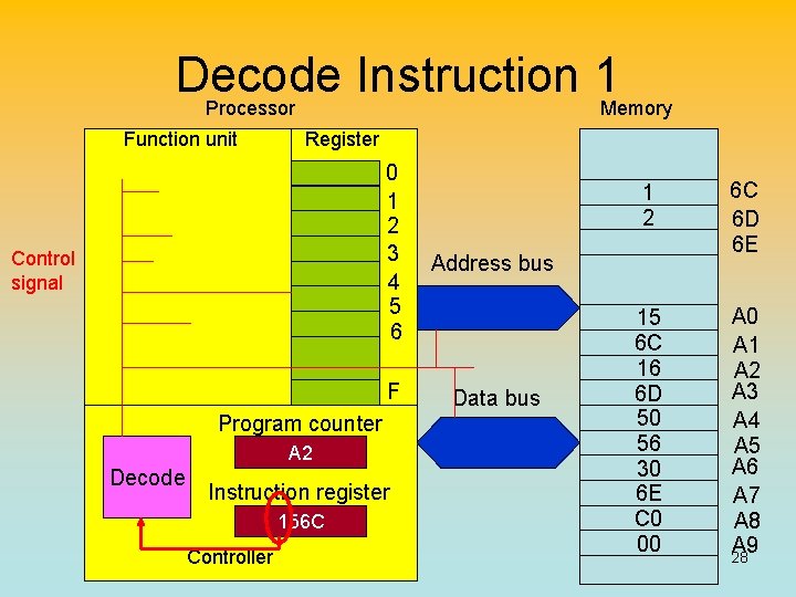
Decode Instruction 1 Processor Memory Function unit Register Control signal 0 1 2 3 4 5 6 Address bus F Data bus Program counter A 2 Decode Instruction register 156 C Controller 1 2 6 C 6 D 6 E 15 6 C 16 6 D 50 56 30 6 E C 0 00 A 1 A 2 A 3 A 4 A 5 A 6 A 7 A 8 A 9 28

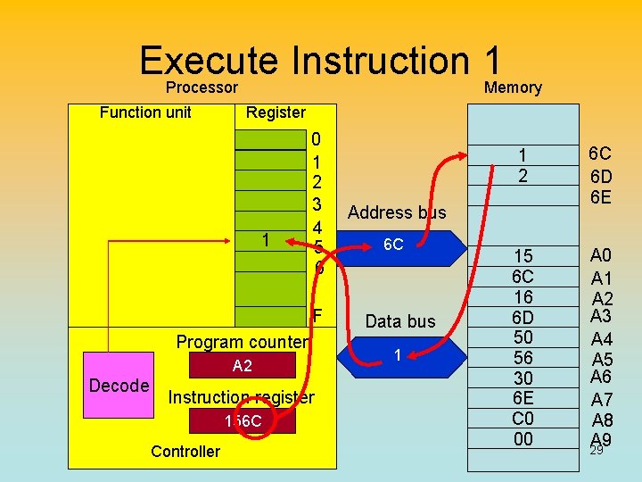
Execute Instruction 1 Processor Memory Function unit Register 1 0 1 2 3 4 5 6 Address bus F Data bus Program counter A 2 Decode Instruction register 156 C Controller 6 C 1 1 2 6 C 6 D 6 E 15 6 C 16 6 D 50 56 30 6 E C 0 00 A 1 A 2 A 3 A 4 A 5 A 6 A 7 A 8 A 9 29

Fetch Instruction 2 Processor Memory Function unit Register 1 0 1 2 3 4 5 6 Address bus F Data bus Program counter A 4 A 2 Instruction register 166 D Controller A 2 166 D 1 2 6 C 6 D 6 E 15 6 C 16 6 D 50 56 30 6 E C 0 00 A 1 A 2 A 3 A 4 A 5 A 6 A 7 A 8 A 9 30

Decode Instruction 2 Processor Memory Function unit Register 1 0 1 2 3 4 5 6 Address bus F Data bus Program counter A 4 Decode Instruction register 166 D Controller 1 2 6 C 6 D 6 E 15 6 C 16 6 D 50 56 30 6 E C 0 00 A 1 A 2 A 3 A 4 A 5 A 6 A 7 A 8 A 9 31

Execute Instruction 2 Processor Memory Function unit Register 1 2 0 1 2 3 4 5 6 Address bus F Data bus Program counter A 4 Decode Instruction register 166 D Controller 6 D 2 1 2 6 C 6 D 6 E 15 6 C 16 6 D 50 56 30 6 E C 0 00 A 1 A 2 A 3 A 4 A 5 A 6 A 7 A 8 A 9 32

Fetch Instruction 3 Processor Memory Function unit Register 1 2 0 1 2 3 4 5 6 Address bus F Data bus Program counter A 4 A 6 Instruction register 5056 Controller A 4 5056 1 2 6 C 6 D 6 E 15 6 C 16 6 D 50 56 30 6 E C 0 00 A 1 A 2 A 3 A 4 A 5 A 6 A 7 A 8 A 9 33

Decode Instruction 3 Processor Memory Function unit Register 1 2 0 1 2 3 4 5 6 Address bus F Data bus Program counter A 6 Decode Instruction register 5056 Controller 1 2 6 C 6 D 6 E 15 6 C 16 6 D 50 56 30 6 E C 0 00 A 1 A 2 A 3 A 4 A 5 A 6 A 7 A 8 A 9 34

Execute Instruction 3 Processor Memory Function unit Register 3 Adder 1 2 0 1 2 3 4 5 6 Address bus F Data bus Program counter A 6 Decode Instruction register 5056 Controller 1 2 6 C 6 D 6 E 15 6 C 16 6 D 50 56 30 6 E C 0 00 A 1 A 2 A 3 A 4 A 5 A 6 A 7 A 8 A 9 35

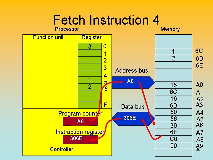
Fetch Instruction 4 Processor Memory Function unit Register 3 1 2 0 1 2 3 4 5 6 Address bus F Data bus Program counter A 8 A 6 Instruction register 306 E Controller A 6 306 E 1 2 6 C 6 D 6 E 15 6 C 16 6 D 50 56 30 6 E C 0 00 A 1 A 2 A 3 A 4 A 5 A 6 A 7 A 8 A 9 36

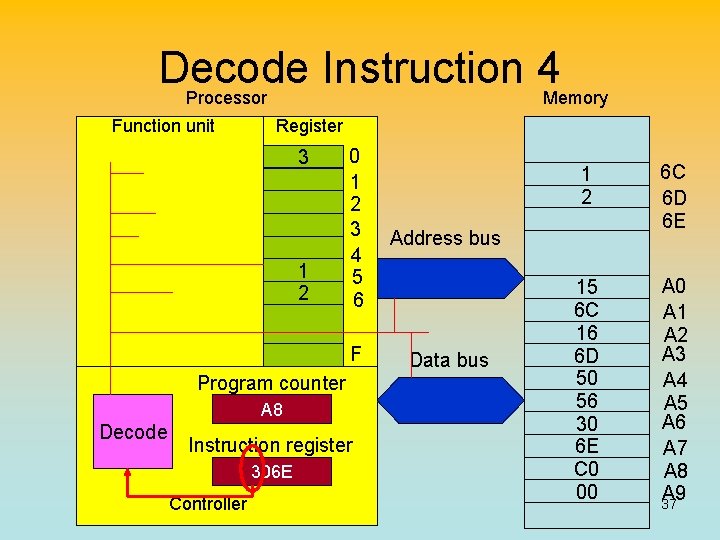
Decode Instruction 4 Processor Memory Function unit Register 3 1 2 0 1 2 3 4 5 6 Address bus F Data bus Program counter A 8 Decode Instruction register 306 E Controller 1 2 6 C 6 D 6 E 15 6 C 16 6 D 50 56 30 6 E C 0 00 A 1 A 2 A 3 A 4 A 5 A 6 A 7 A 8 A 9 37

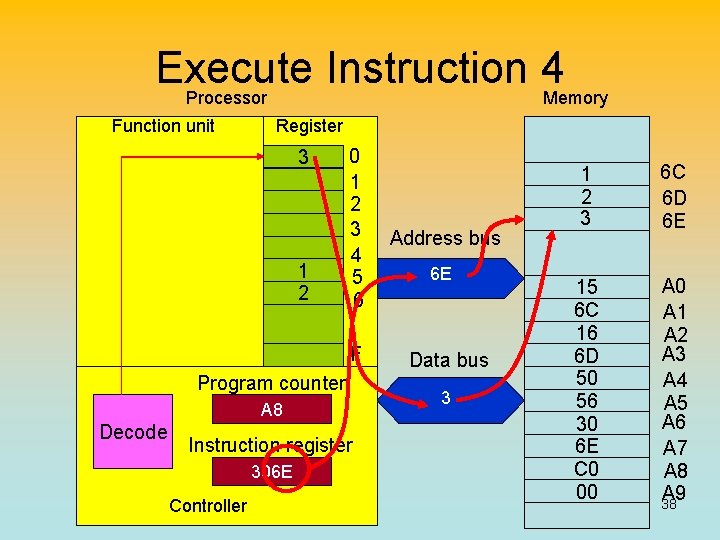
Execute Instruction 4 Processor Memory Function unit Register 3 1 2 0 1 2 3 4 5 6 Address bus F Data bus Program counter A 8 Decode Instruction register 306 E Controller 6 E 3 1 2 3 6 C 6 D 6 E 15 6 C 16 6 D 50 56 30 6 E C 0 00 A 1 A 2 A 3 A 4 A 5 A 6 A 7 A 8 A 9 38

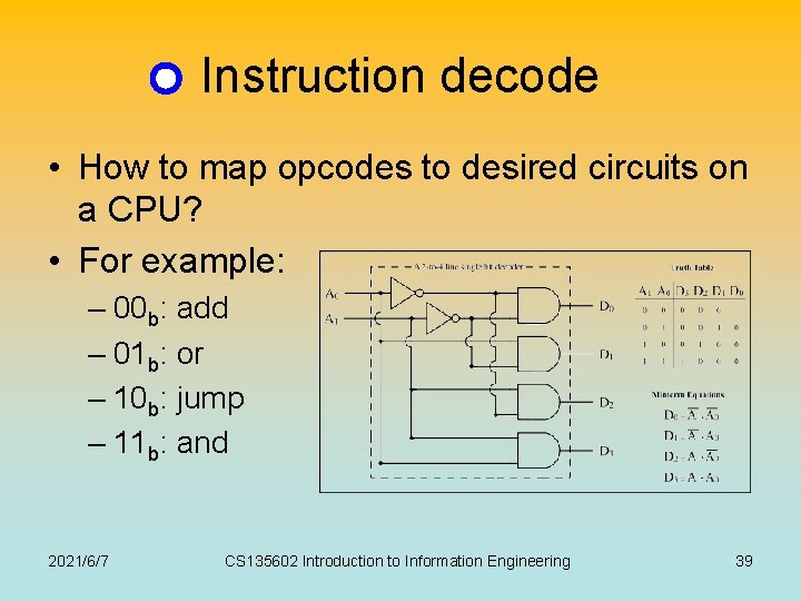
Instruction decode • How to map opcodes to desired circuits on a CPU? • For example: – 00 b: add – 01 b: or – 10 b: jump – 11 b: and 2021/6/7 CS 135602 Introduction to Information Engineering 39

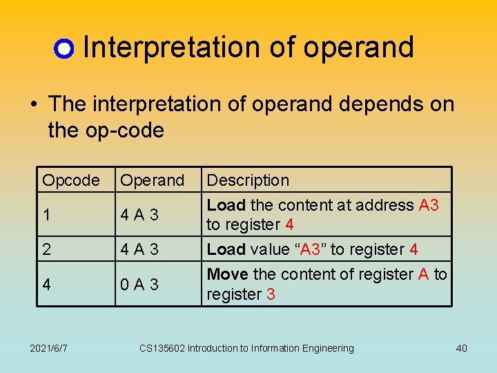
Interpretation of operand • The interpretation of operand depends on the op-code Operand 1 4 A 3 2 4 A 3 4 0 A 3 2021/6/7 Description Load the content at address A 3 to register 4 Load value “A 3” to register 4 Move the content of register A to register 3 CS 135602 Introduction to Information Engineering 40

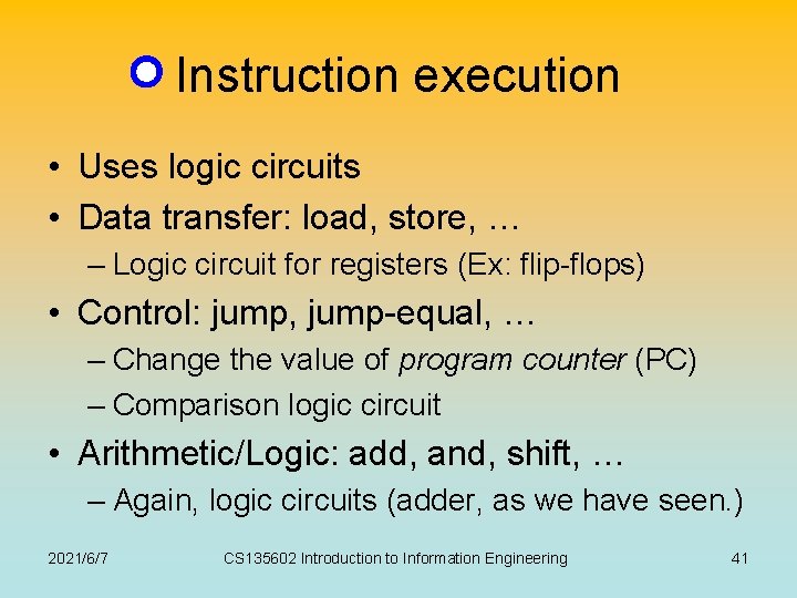
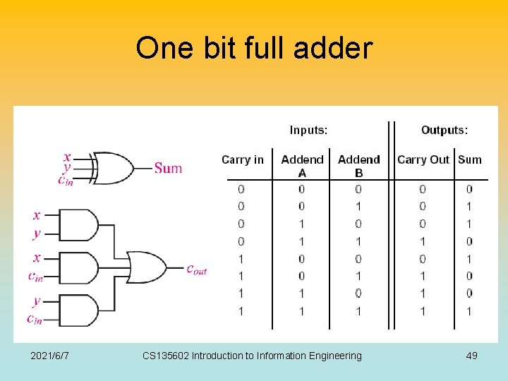
Instruction execution • Uses logic circuits • Data transfer: load, store, … – Logic circuit for registers (Ex: flip-flops) • Control: jump, jump-equal, … – Change the value of program counter (PC) – Comparison logic circuit • Arithmetic/Logic: add, and, shift, … – Again, logic circuits (adder, as we have seen. ) 2021/6/7 CS 135602 Introduction to Information Engineering 41

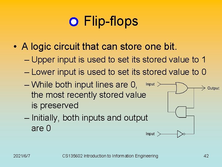
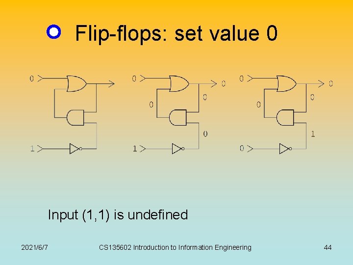
Flip-flops • A logic circuit that can store one bit. – Upper input is used to set its stored value to 1 – Lower input is used to set its stored value to 0 – While both input lines are 0, the most recently stored value is preserved – Initially, both inputs and output are 0 2021/6/7 CS 135602 Introduction to Information Engineering 42

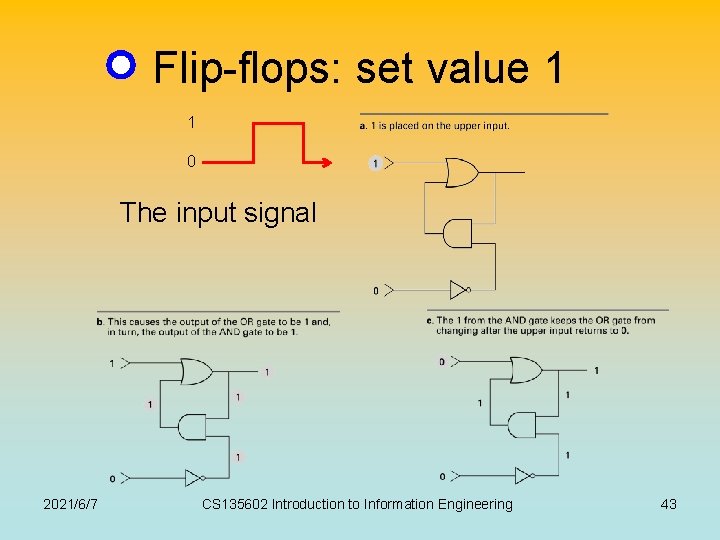
Flip-flops: set value 1 1 0 The input signal 2021/6/7 CS 135602 Introduction to Information Engineering 43

Flip-flops: set value 0 Input (1, 1) is undefined 2021/6/7 CS 135602 Introduction to Information Engineering 44

Example of jump • JUMP to instruction at address 58 H if the content of register 2 is the same as that of register 0 2021/6/7 CS 135602 Introduction to Information Engineering 45

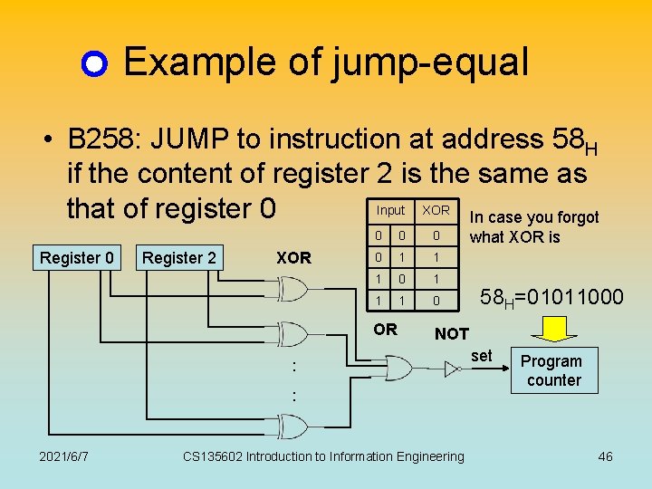
Example of jump-equal • B 258: JUMP to instruction at address 58 H if the content of register 2 is the same as Input XOR that of register 0 In case you forgot Register 0 Register 2 XOR 0 0 1 1 1 0 OR 58 H=01011000 NOT : : 2021/6/7 what XOR is CS 135602 Introduction to Information Engineering set Program counter 46

Arithmetic/Logic Operations 2021/6/7 CS 135602 Introduction to Information Engineering 47

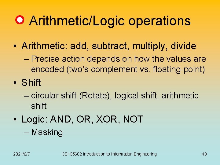
Arithmetic/Logic operations • Arithmetic: add, subtract, multiply, divide – Precise action depends on how the values are encoded (two’s complement vs. floating-point) • Shift – circular shift (Rotate), logical shift, arithmetic shift • Logic: AND, OR, XOR, NOT – Masking 2021/6/7 CS 135602 Introduction to Information Engineering 48

One bit full adder 2021/6/7 CS 135602 Introduction to Information Engineering 49

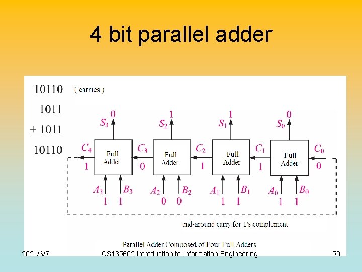
4 bit parallel adder 2021/6/7 CS 135602 Introduction to Information Engineering 50

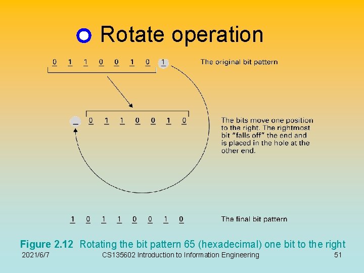
Rotate operation Figure 2. 12 Rotating the bit pattern 65 (hexadecimal) one bit to the right 2021/6/7 CS 135602 Introduction to Information Engineering 51

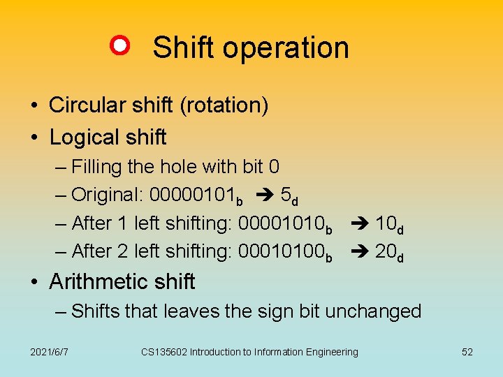
Shift operation • Circular shift (rotation) • Logical shift – Filling the hole with bit 0 – Original: 00000101 b 5 d – After 1 left shifting: 00001010 b 10 d – After 2 left shifting: 00010100 b 20 d • Arithmetic shift – Shifts that leaves the sign bit unchanged 2021/6/7 CS 135602 Introduction to Information Engineering 52

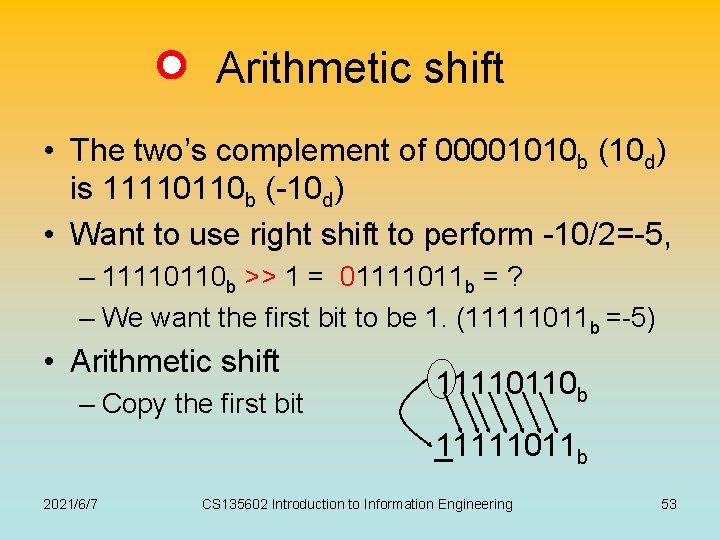
Arithmetic shift • The two’s complement of 00001010 b (10 d) is 11110110 b (-10 d) • Want to use right shift to perform -10/2=-5, – 11110110 b >> 1 = 01111011 b = ? – We want the first bit to be 1. (11111011 b =-5) • Arithmetic shift – Copy the first bit 11110110 b _1111011 1 b 2021/6/7 CS 135602 Introduction to Information Engineering 53

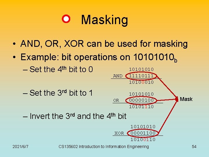
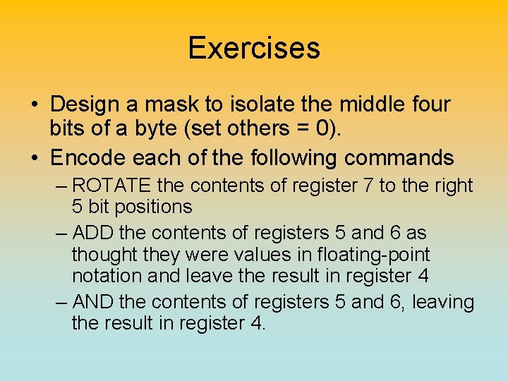
Masking • AND, OR, XOR can be used for masking • Example: bit operations on 1010 b – Set the 4 th bit to 0 AND 1010 11110111 10100010 OR 1010 00000100 10101110 – Set the 3 rd bit to 1 Mask – Invert the 3 rd and the 4 th bit XOR 2021/6/7 1010 00001100 10100110 CS 135602 Introduction to Information Engineering 54

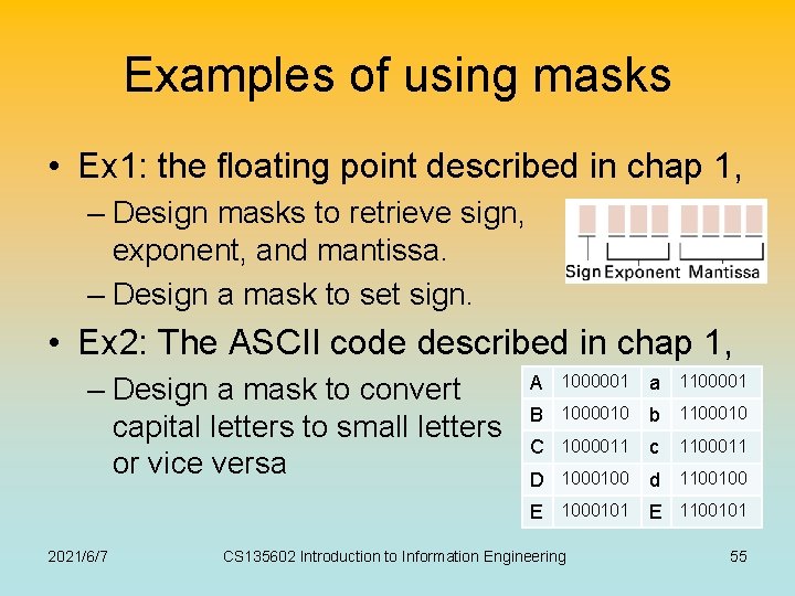
Examples of using masks • Ex 1: the floating point described in chap 1, – Design masks to retrieve sign, exponent, and mantissa. – Design a mask to set sign. • Ex 2: The ASCII code described in chap 1, – Design a mask to convert capital letters to small letters or vice versa 2021/6/7 A 1000001 a 1100001 B 1000010 b 1100010 C 1000011 c 1100011 D 1000100 d 1100100 E 1000101 E 1100101 CS 135602 Introduction to Information Engineering 55

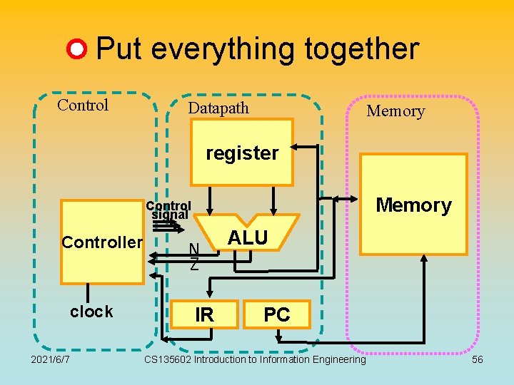
Put everything together Control Datapath Memory register Memory Control signal Controller clock 2021/6/7 N Z IR ALU PC CS 135602 Introduction to Information Engineering 56

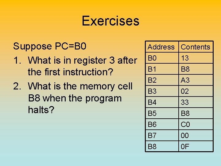
Exercises Suppose PC=B 0 1. What is in register 3 after the first instruction? 2. What is the memory cell B 8 when the program halts? Address B 0 B 1 B 2 Contents 13 B 8 A 3 B 4 B 5 B 6 B 7 B 8 02 33 B 8 C 0 00 0 F

Exercises • Design a mask to isolate the middle four bits of a byte (set others = 0). • Encode each of the following commands – ROTATE the contents of register 7 to the right 5 bit positions – ADD the contents of registers 5 and 6 as thought they were values in floating-point notation and leave the result in register 4 – AND the contents of registers 5 and 6, leaving the result in register 4.

Peripheral Devices 2021/6/7 CS 135602 Introduction to Information Engineering 59

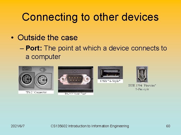
Connecting to other devices • Outside the case – Port: The point at which a device connects to a computer 2021/6/7 CS 135602 Introduction to Information Engineering 60

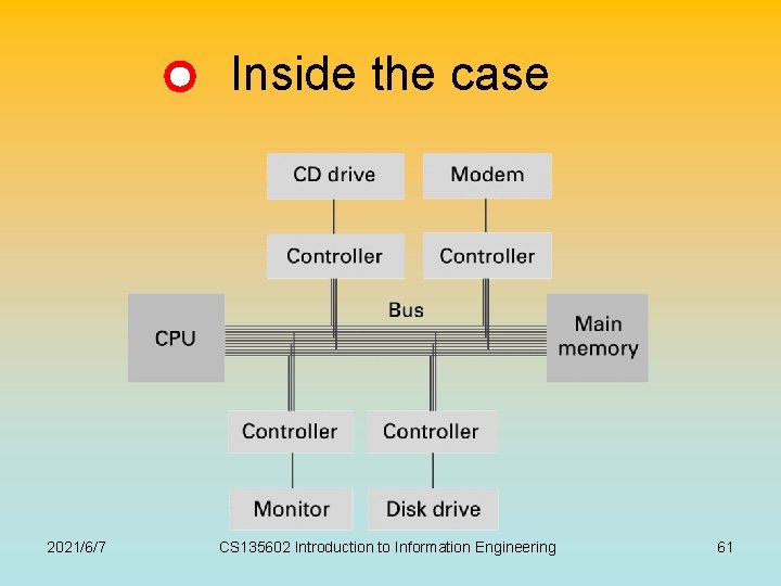
Inside the case 2021/6/7 CS 135602 Introduction to Information Engineering 61

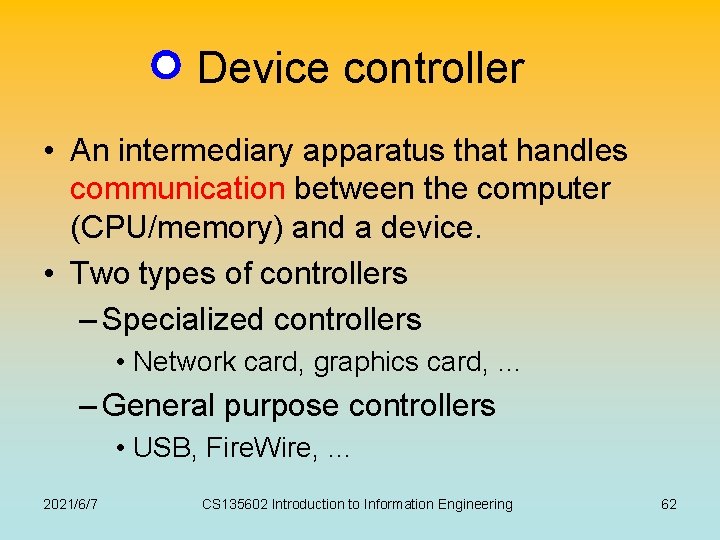
Device controller • An intermediary apparatus that handles communication between the computer (CPU/memory) and a device. • Two types of controllers – Specialized controllers • Network card, graphics card, … – General purpose controllers • USB, Fire. Wire, … 2021/6/7 CS 135602 Introduction to Information Engineering 62

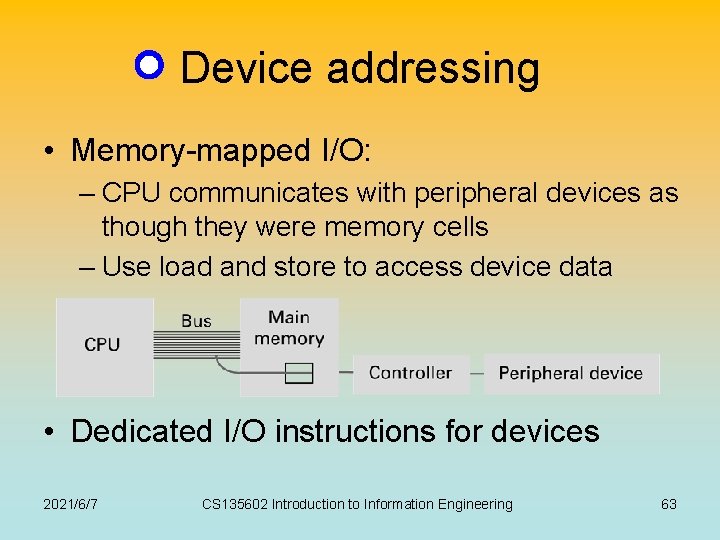
Device addressing • Memory-mapped I/O: – CPU communicates with peripheral devices as though they were memory cells – Use load and store to access device data • Dedicated I/O instructions for devices 2021/6/7 CS 135602 Introduction to Information Engineering 63

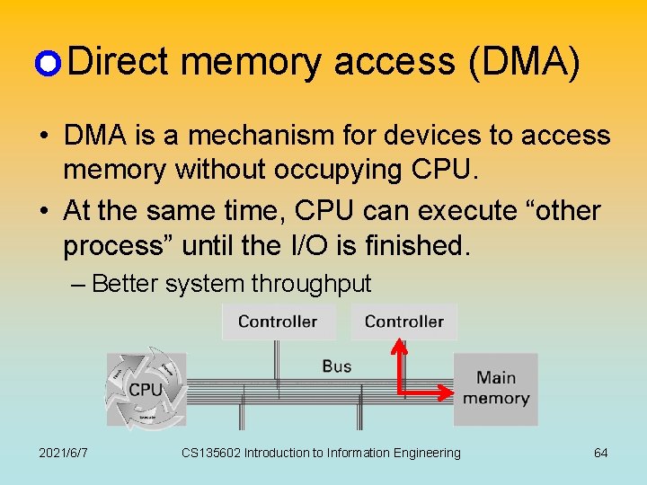
Direct memory access (DMA) • DMA is a mechanism for devices to access memory without occupying CPU. • At the same time, CPU can execute “other process” until the I/O is finished. – Better system throughput 2021/6/7 CS 135602 Introduction to Information Engineering 64

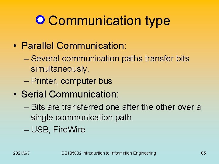
Communication type • Parallel Communication: – Several communication paths transfer bits simultaneously. – Printer, computer bus • Serial Communication: – Bits are transferred one after the other over a single communication path. – USB, Fire. Wire 2021/6/7 CS 135602 Introduction to Information Engineering 65

Exercises • Suppose the machine use memory I/O and the memory address B 5 is the location within the printer port to which data to be printed. If register 7 contains the ASCII code for the letter A, what instruction can make letter A to be printed? • If a printer can only print 128 characters per second, and has local buffer of 256 KB, how fast the data rate (bps) can be?

Parallel Architectures 2021/6/7 CS 135602 Introduction to Information Engineering 67

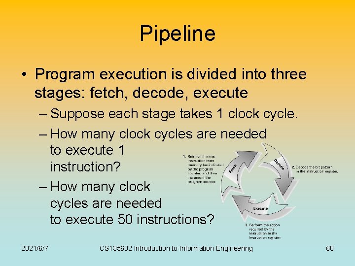
Pipeline • Program execution is divided into three stages: fetch, decode, execute – Suppose each stage takes 1 clock cycle. – How many clock cycles are needed to execute 1 instruction? – How many clock cycles are needed to execute 50 instructions? 2021/6/7 CS 135602 Introduction to Information Engineering 68

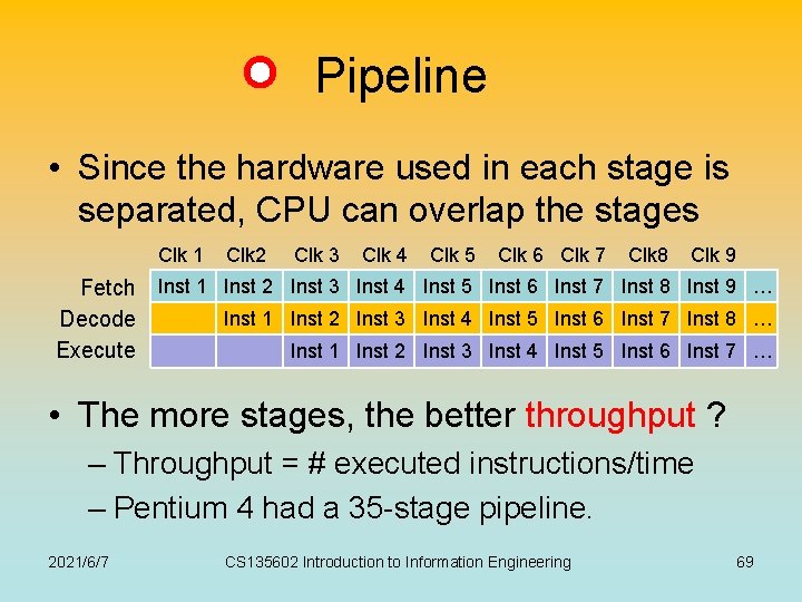
Pipeline • Since the hardware used in each stage is separated, CPU can overlap the stages Clk 1 Fetch Decode Execute Clk 2 Clk 3 Clk 4 Clk 5 Clk 6 Clk 7 Clk 8 Clk 9 Inst 1 Inst 2 Inst 3 Inst 4 Inst 5 Inst 6 Inst 7 Inst 8 Inst 9 … Inst 1 Inst 2 Inst 3 Inst 4 Inst 5 Inst 6 Inst 7 Inst 8 … Inst 1 Inst 2 Inst 3 Inst 4 Inst 5 Inst 6 Inst 7 … • The more stages, the better throughput ? – Throughput = # executed instructions/time – Pentium 4 had a 35 -stage pipeline. 2021/6/7 CS 135602 Introduction to Information Engineering 69

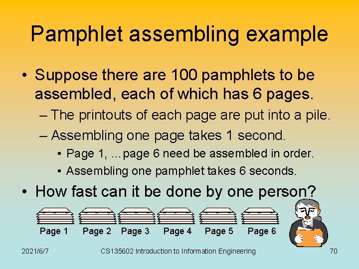
Pamphlet assembling example • Suppose there are 100 pamphlets to be assembled, each of which has 6 pages. – The printouts of each page are put into a pile. – Assembling one page takes 1 second. • Page 1, …page 6 need be assembled in order. • Assembling one pamphlet takes 6 seconds. • How fast can it be done by one person? Page 1 2021/6/7 Page 2 Page 3 Page 4 Page 5 Page 6 CS 135602 Introduction to Information Engineering 70

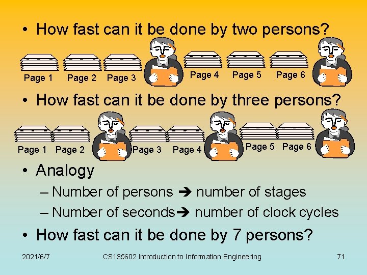
• How fast can it be done by two persons? Page 1 Page 2 Page 3 Page 4 Page 5 Page 6 • How fast can it be done by three persons? Page 1 Page 2 Page 3 Page 4 Page 5 Page 6 • Analogy – Number of persons number of stages – Number of seconds number of clock cycles • How fast can it be done by 7 persons? 2021/6/7 CS 135602 Introduction to Information Engineering 71

Clock cycle/clock rate • The basic time unit of a CPU – For example, a 2 GHz CPU has clock cycle 1/2 G = 5× 10 -10 second. • 2 GHz is the “clock rate” of a CPU. – Every operation in CPU takes the time that is a multiple of the clock cycle. 2021/6/7 CS 135602 Introduction to Information Engineering 72

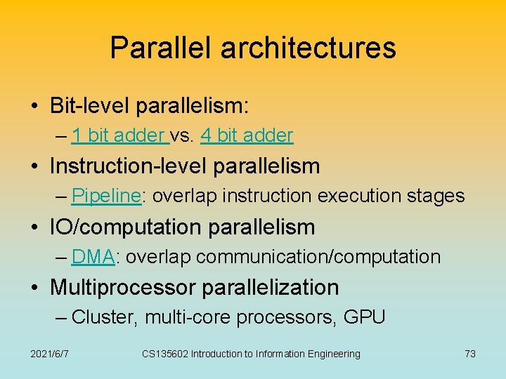
Parallel architectures • Bit-level parallelism: – 1 bit adder vs. 4 bit adder • Instruction-level parallelism – Pipeline: overlap instruction execution stages • IO/computation parallelism – DMA: overlap communication/computation • Multiprocessor parallelization – Cluster, multi-core processors, GPU 2021/6/7 CS 135602 Introduction to Information Engineering 73

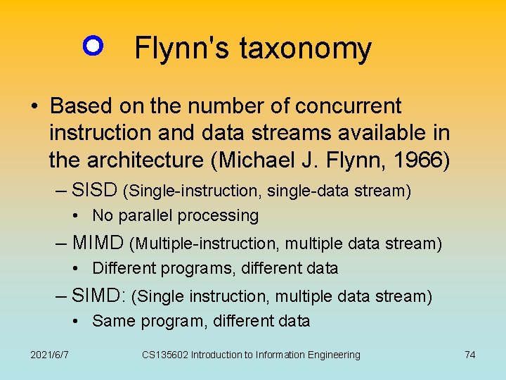
Flynn's taxonomy • Based on the number of concurrent instruction and data streams available in the architecture (Michael J. Flynn, 1966) – SISD (Single-instruction, single-data stream) • No parallel processing – MIMD (Multiple-instruction, multiple data stream) • Different programs, different data – SIMD: (Single instruction, multiple data stream) • Same program, different data 2021/6/7 CS 135602 Introduction to Information Engineering 74
![SIMD example SISD forloop fori0 i5 i AiBiCi SIMD expansion SIMD example • SISD for-loop – for(i=0; i<5; i++) A[i]=B[i]+C[i]; • SIMD expansion –](https://slidetodoc.com/presentation_image_h2/5d3e150f9bdc5fcc4f1729e0ab9ef444/image-75.jpg)
SIMD example • SISD for-loop – for(i=0; i<5; i++) A[i]=B[i]+C[i]; • SIMD expansion – CPU 1: – CPU 2: – CPU 3: – CPU 4: – CPU 5: 2021/6/7 A[0]=B[0]+C[0]; A[1]=B[1]+C[1]; A[2]=B[2]+C[2]; A[3]=B[3]+C[3]; A[4]=B[4]+C[4]; CS 135602 Introduction to Information Engineering 75

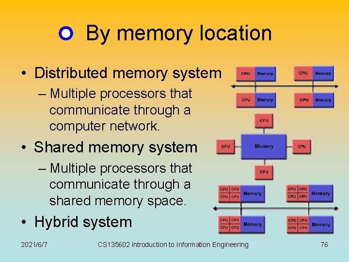
By memory location • Distributed memory system – Multiple processors that communicate through a computer network. • Shared memory system – Multiple processors that communicate through a shared memory space. • Hybrid system 2021/6/7 CS 135602 Introduction to Information Engineering 76

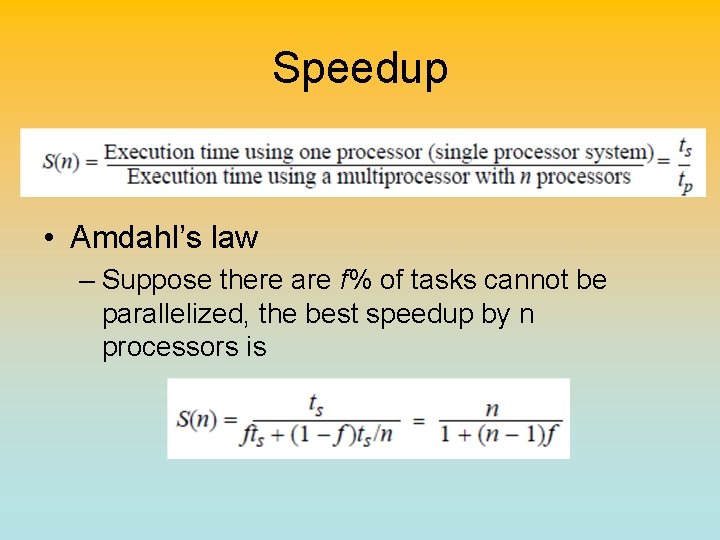
Speedup • Amdahl’s law – Suppose there are f% of tasks cannot be parallelized, the best speedup by n processors is

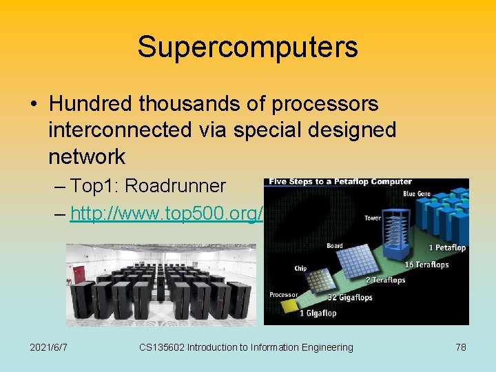
Supercomputers • Hundred thousands of processors interconnected via special designed network – Top 1: Roadrunner – http: //www. top 500. org/ 2021/6/7 CS 135602 Introduction to Information Engineering 78

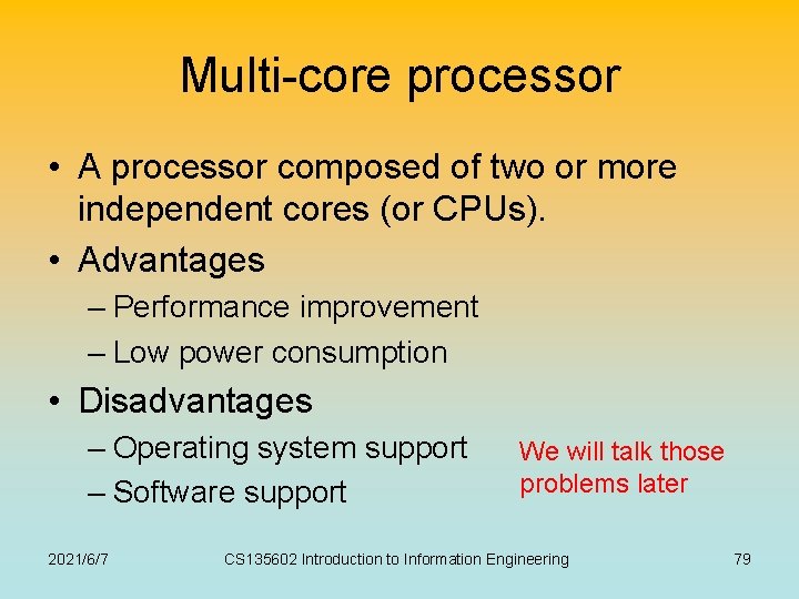
Multi-core processor • A processor composed of two or more independent cores (or CPUs). • Advantages – Performance improvement – Low power consumption • Disadvantages – Operating system support – Software support 2021/6/7 We will talk those problems later CS 135602 Introduction to Information Engineering 79

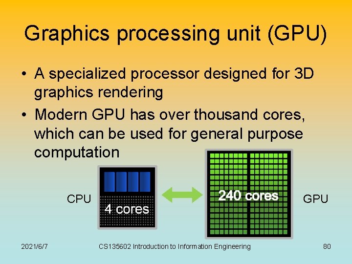
Graphics processing unit (GPU) • A specialized processor designed for 3 D graphics rendering • Modern GPU has over thousand cores, which can be used for general purpose computation CPU 2021/6/7 GPU CS 135602 Introduction to Information Engineering 80

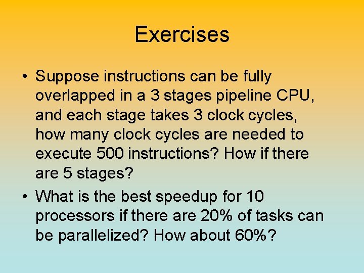
Exercises • Suppose instructions can be fully overlapped in a 3 stages pipeline CPU, and each stage takes 3 clock cycles, how many clock cycles are needed to execute 500 instructions? How if there are 5 stages? • What is the best speedup for 10 processors if there are 20% of tasks can be parallelized? How about 60%?

Related courses • Store program concept, peripheral devices – 計算機結構,硬體實驗,微算機系統,邏輯設計,嵌入 式系統概論 • Parallel Architectures References • http: //www. top 500. org/ (supercomputer) • https: //computing. llnl. gov/tutorials/parallel_comp/ • www. cs. nthu. edu. tw/~ychung/slides/para_programming/slides 1. pdf • Textbook chap 2 2021/6/7 CS 135602 Introduction to Information Engineering 82

Opcode Operand Description 1 RXY LOAD the register R with the bit pattern found in the memory cell whose address is XY. Example: I 4 A 3 would cause the contents of the memory cell located at address A 3 to be placed in register 4. 2 RXY LOAD the register R with the bit pattern XY. Example: 20 A 3 would cause the value A 3 to be placed in register 0. 3 RST STORE the bit pattern found in register R in the memory cell whose address is XY. Example: 35 B 1 would cause the contents of register 5 to be placed in the memory cell whose address is B 1. 4 ORS MOVE the bit pattern found in register R to register S. Example: 40 A 4 would cause the contents of register A to be copied into register 4. 5 RST ADD the bit patterns in registers S and T as though they were two's complement representations and leave the result in register R. Example: 5726 would cause the binary values in registers 2 and 6 to be added and the sum placed in register 7.

Opcode Operand Description 6 RST ADD the bit patterns in registers S and T as though they represented values in floating point notation and leave the floating-point result in register R. Example: 634 E would cause the values in registers 4 and E to be added as floating-point values and the result to be placed in register 3. 7 RST OR the bit patterns in registers S and T and place the result in register R. Example: 7 CB 4 would cause the result of ORing the contents of registers Band 4 to be placed in register C. 8 RST AND the bit patterns in registers S and T and place the result in register R. Example: 8045 would cause the result of ANDing the contents of registers 4 and 5 to be placed in register 0. 9 RST EXCLUSIVE OR the bit patterns in registers Sand T and place the result in register R. Example: 95 F 3 would cause the result of EXCLUSIVE ORing the contents of registers F and 3 to be placed in register 5

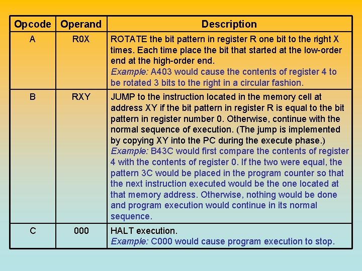
Opcode Operand Description A R 0 X ROTATE the bit pattern in register R one bit to the right X times. Each time place the bit that started at the low-order end at the high-order end. Example: A 403 would cause the contents of register 4 to be rotated 3 bits to the right in a circular fashion. B RXY JUMP to the instruction located in the memory cell at address XY if the bit pattern in register R is equal to the bit pattern in register number 0. Otherwise, continue with the normal sequence of execution. (The jump is implemented by copying XY into the PC during the execute phase. ) Example: B 43 C would first compare the contents of register 4 with the contents of register 0. If the two were equal, the pattern 3 C would be placed in the program counter so that the next instruction executed would be the one located at that memory address. Otherwise, nothing would be done and program execution would continue in its normal sequence. C 000 HALT execution. Example: C 000 would cause program execution to stop.