CPU Sequencing 672021 1 Instruction Cycles Machine Cycles

- Slides: 24

CPU Sequencing 6/7/2021 1

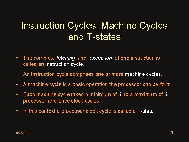
Instruction Cycles, Machine Cycles and T-states • The complete fetching and execution of one instruction is called an instruction cycle. • An instruction cycle comprises one or more machine cycles. • A machine cycle is a basic operation the processor can perform. • Each machine cycle takes a minimum of 3 to a maximum of 6 processor reference clock cycles. • In this context a processor clock cycle is called a T-state 6/7/2021 2

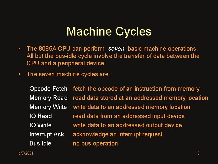
Machine Cycles • The 8085 A CPU can perform seven basic machine operations. All but the bus-idle cycle involve the transfer of data between the CPU and a peripheral device. • The seven machine cycles are : Opcode Fetch Memory Read Memory Write IO Read IO Write Interrupt Ack Bus Idle 6/7/2021 fetch the opcode of an instruction from memory read data stored at an addressed memory location write data to an addressed memory location read data from an addressed input device write data to an addressed output device acknowledge an interrupt request no bus operation 3

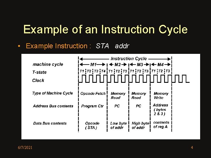
Example of an Instruction Cycle • Example Instruction : STA addr 6/7/2021 4

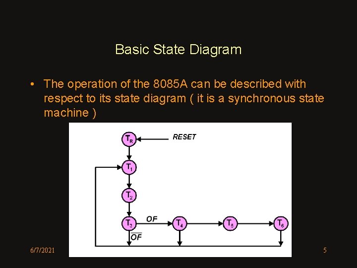
Basic State Diagram • The operation of the 8085 A can be described with respect to its state diagram ( it is a synchronous state machine ) 6/7/2021 5

Basic State Diagram • Irrespective of the particular machine cycle the processor is performing, the 8085 A performs basically the same tasks during each T-state. • The Tr-state is the state the machine enters following a hardware reset to the processor. • For all machine cycles, other than opcode fetch, the state sequence is T 1 T 2 T 3 T 1 • For opcode fetch machine cycles, the state sequence is T 1 T 2 T 3 T 4 T 1 or T 1 T 2 T 3 T 4 T 5 T 6 T 1 depending on the instruction. 6/7/2021 6

Opcode Fetch Machine Cycle 6/7/2021 7

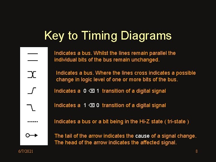
Key to Timing Diagrams Indicates a bus. Whilst the lines remain parallel the individual bits of the bus remain unchanged. Indicates a bus. Where the lines cross indicates a possible change in logic level of one or more bits of the bus. Indicates a 0 1 transition of a digital signal Indicates a 1 0 transition of a digital signal Indicates a bus or a bit being in the Hi-Z state ( tri-state ) The tail of the arrow indicates the cause of a signal change. The head of the arrow indicates the affected signal. 6/7/2021 8

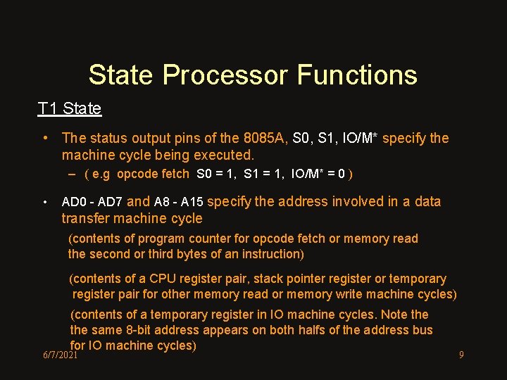
State Processor Functions T 1 State • The status output pins of the 8085 A, S 0, S 1, IO/M* specify the machine cycle being executed. – ( e. g opcode fetch S 0 = 1, S 1 = 1, IO/M* = 0 ) • AD 0 - AD 7 and A 8 - A 15 specify the address involved in a data transfer machine cycle (contents of program counter for opcode fetch or memory read the second or third bytes of an instruction) (contents of a CPU register pair, stack pointer register or temporary register pair for other memory read or memory write machine cycles) (contents of a temporary register in IO machine cycles. Note the same 8 -bit address appears on both halfs of the address bus for IO machine cycles) 6/7/2021 9

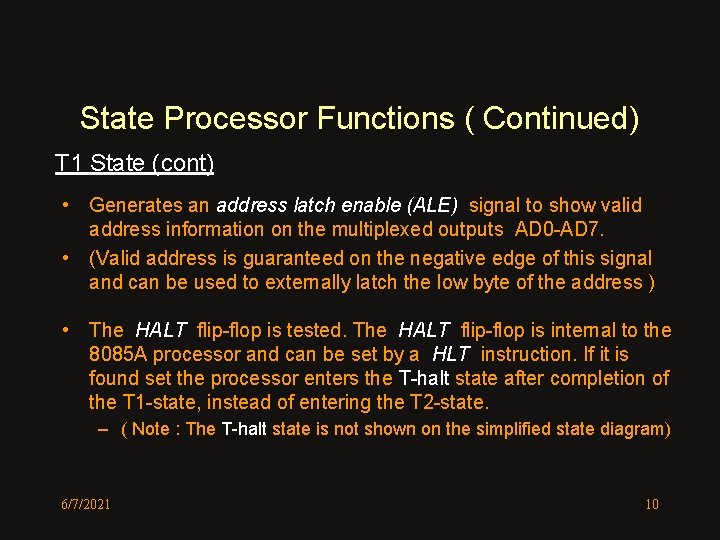
State Processor Functions ( Continued) T 1 State (cont) • Generates an address latch enable (ALE) signal to show valid address information on the multiplexed outputs AD 0 -AD 7. • (Valid address is guaranteed on the negative edge of this signal and can be used to externally latch the low byte of the address ) • The HALT flip-flop is tested. The HALT flip-flop is internal to the 8085 A processor and can be set by a HLT instruction. If it is found set the processor enters the T-halt state after completion of the T 1 -state, instead of entering the T 2 -state. – ( Note : The T-halt state is not shown on the simplified state diagram) 6/7/2021 10

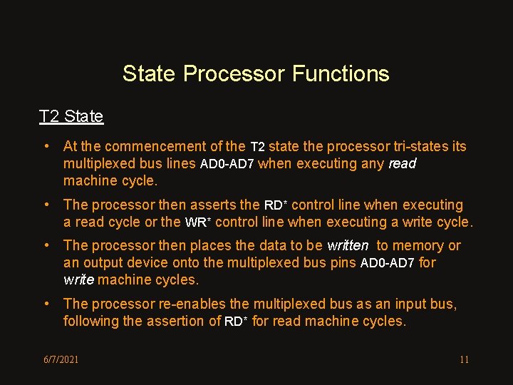
State Processor Functions T 2 State • At the commencement of the T 2 state the processor tri-states its multiplexed bus lines AD 0 -AD 7 when executing any read machine cycle. • The processor then asserts the RD* control line when executing a read cycle or the WR* control line when executing a write cycle. • The processor then places the data to be written to memory or an output device onto the multiplexed bus pins AD 0 -AD 7 for write machine cycles. • The processor re-enables the multiplexed bus as an input bus, following the assertion of RD* for read machine cycles. 6/7/2021 11

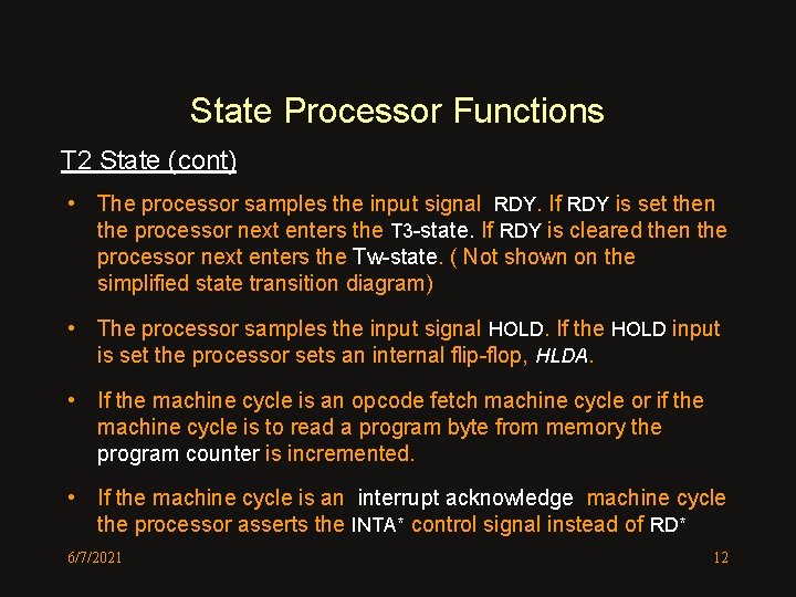
State Processor Functions T 2 State (cont) • The processor samples the input signal RDY. If RDY is set then the processor next enters the T 3 -state. If RDY is cleared then the processor next enters the Tw-state. ( Not shown on the simplified state transition diagram) • The processor samples the input signal HOLD. If the HOLD input is set the processor sets an internal flip-flop, HLDA. • If the machine cycle is an opcode fetch machine cycle or if the machine cycle is to read a program byte from memory the program counter is incremented. • If the machine cycle is an interrupt acknowledge machine cycle the processor asserts the INTA* control signal instead of RD* 6/7/2021 12

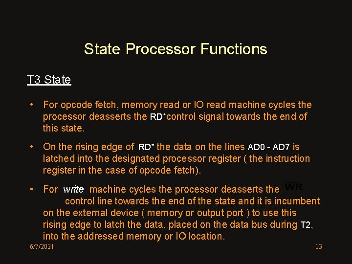
State Processor Functions T 3 State • For opcode fetch, memory read or IO read machine cycles the processor deasserts the RD*control signal towards the end of this state. • On the rising edge of RD* the data on the lines AD 0 - AD 7 is latched into the designated processor register ( the instruction register in the case of opcode fetch). • For write machine cycles the processor deasserts the control line towards the end of the state and it is incumbent on the external device ( memory or output port ) to use this rising edge to latch the data, placed on the data bus during T 2, into the addressed memory or IO location. 6/7/2021 13

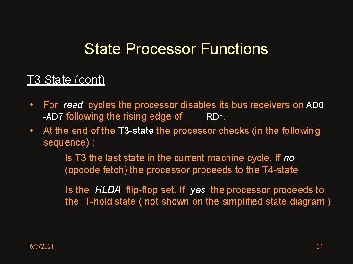
State Processor Functions T 3 State (cont) • For read cycles the processor disables its bus receivers on AD 0 -AD 7 following the rising edge of RD*. • At the end of the T 3 -state the processor checks (in the following sequence) : Is T 3 the last state in the current machine cycle. If no (opcode fetch) the processor proceeds to the T 4 -state Is the HLDA flip-flop set. If yes the processor proceeds to the T-hold state ( not shown on the simplified state diagram ) 6/7/2021 14

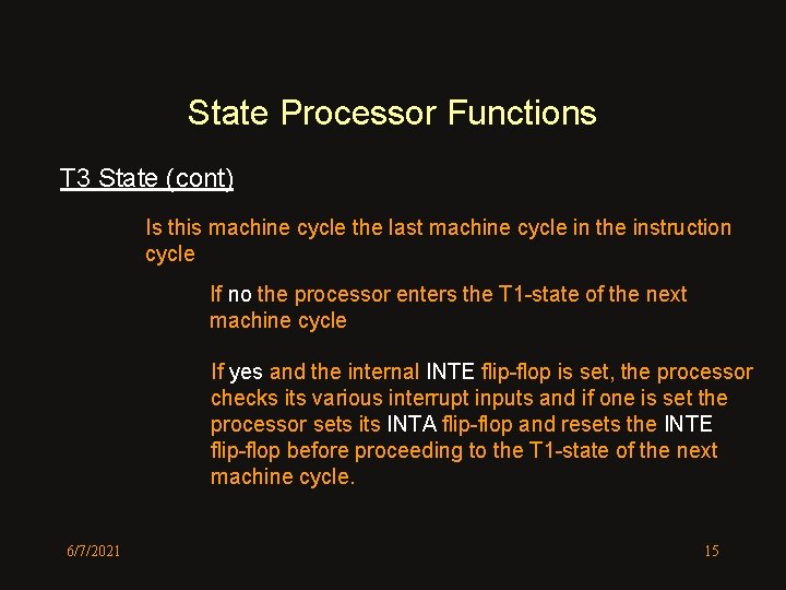
State Processor Functions T 3 State (cont) Is this machine cycle the last machine cycle in the instruction cycle If no the processor enters the T 1 -state of the next machine cycle If yes and the internal INTE flip-flop is set, the processor checks its various interrupt inputs and if one is set the processor sets its INTA flip-flop and resets the INTE flip-flop before proceeding to the T 1 -state of the next machine cycle. 6/7/2021 15

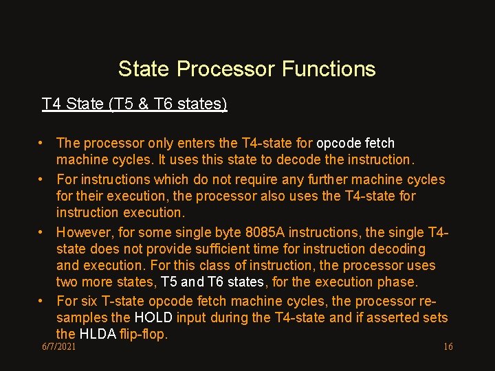
State Processor Functions T 4 State (T 5 & T 6 states) • The processor only enters the T 4 -state for opcode fetch machine cycles. It uses this state to decode the instruction. • For instructions which do not require any further machine cycles for their execution, the processor also uses the T 4 -state for instruction execution. • However, for some single byte 8085 A instructions, the single T 4 state does not provide sufficient time for instruction decoding and execution. For this class of instruction, the processor uses two more states, T 5 and T 6 states, for the execution phase. • For six T-state opcode fetch machine cycles, the processor resamples the HOLD input during the T 4 -state and if asserted sets the HLDA flip-flop. 6/7/2021 16

6/7/2021 17

Other States HALT-state • The T-halt state is entered after execution of the HLT instruction. The instruction is executed in the T 4 -state of the opcode fetch machine cycle by the processor setting the internal halt flip-flop. • In the T 1 state of the next machine cycle the halt flip-flop is tested and when found asserted the processor enters the T-halt state. • In the halt state the processor checks the hold input signal and the interrupt inputs (provided interrupts are enabled) • If the hold input becomes asserted the processor sets the HLDA flipflop and then enters the hold state, where it remains until the hold input is deasserted. Following deassertion of the hold input the processor returns to the halt state. 6/7/2021 18

Other States HALT-state (cont ) • If a valid interrupt occurs, when in the halt state, the processor resets the halt flip-flop, sets the inta flip-flop and resets the inte flip-flop ( i. e. disables further interrupts ). • The processor then proceeds to the T 1 -state of the next machine cycle. • Note : Only in response to a valid interrupt can the processor permanently leave the halt state. • Great care must be taken when including halt instructions in a program. 6/7/2021 19

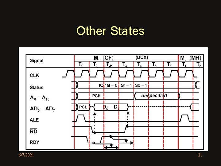
Other States Wait-state • The processor can enter the T-wait state for all machine cycles except the bus idle machine cycle. • If, during the T 2 -state the processor samples the RDY input in the deasserted state, the processor enters the T-wait state at the end of the T 2 -state. • In the T-wait state all bus and control signals remain as of the end of the T 2 -state. • When in the T-wait state, the processor re-samples the RDY input. If it remains de-asserted another wait state ensues where the process is repeated. If, on the other hand, the RDY input is found asserted the T 3 state of the machine cycle is entered. 6/7/2021 20

Other States 6/7/2021 21

Need for T-wait States • Memory and I/O devices require a finite period of time between receiving address and control signals ( read or write ) and accessing the data at the designated address. • Without T-wait states, the processor provides approximately 2. 5 master clock cycles between issuing the address and reading the data bus. • If the peripheral device requires more than 2. 5 clock cycles to access the data, the processor will read invalid data. • When writing data, the processor could write data to the incorrect memory or IO location, if sufficient time is not provided. • The introduction of T-wait states into the machine cycle increases the time available to the peripheral to read or write data. 6/7/2021 22

RDY Input Control Circuit to selectively introduce one wait state : 6/7/2021 23

Hold-state Other States • When an external device requests control of the system busses, it does so by asserting the hold input line to the 8085 A. • The hold input line is sampled by the 8085 A in the T 2 -state, T-4 state and T -halt state and if asserted sets the hlda flip-flop. • The hlda flip-flop is tested in the last t-state of any machine cycle and if set the processor enters the T-hold state. • The processor remains in the T-hold state whilst the hold input remains asserted. The processor tri-states its bus drivers effectively isolating the processor from the system and thereby allowing an external device to have control of the system busses. • When the hold input becomes deasserted, the processor resets the hlda flip -flop, leaves the T-hold state and reassumes execution of machine cycles. 6/7/2021 24