CPE 631 Lecture 07 Cache Design Main Memory
![CPE 631 AM Merging Arrays Example /* Before: 2 sequential arrays */ int val[SIZE]; CPE 631 AM Merging Arrays Example /* Before: 2 sequential arrays */ int val[SIZE];](https://slidetodoc.com/presentation_image_h2/14e267ef5c3e5ecfb19bc4e59d1fd70a/image-28.jpg)
![CPE 631 AM Avoiding Bank Conflicts int x[256][512]; Lots of banks for (j = CPE 631 AM Avoiding Bank Conflicts int x[256][512]; Lots of banks for (j =](https://slidetodoc.com/presentation_image_h2/14e267ef5c3e5ecfb19bc4e59d1fd70a/image-68.jpg)
- Slides: 77

CPE 631 Lecture 07: Cache Design & Main Memory Aleksandar Milenković, milenka@ece. uah. edu Electrical and Computer Engineering University of Alabama in Huntsville

CPE 631 AM Outline Cache Performance n How to Improve Cache Performance n 12/17/2021 UAH-CPE 631 2

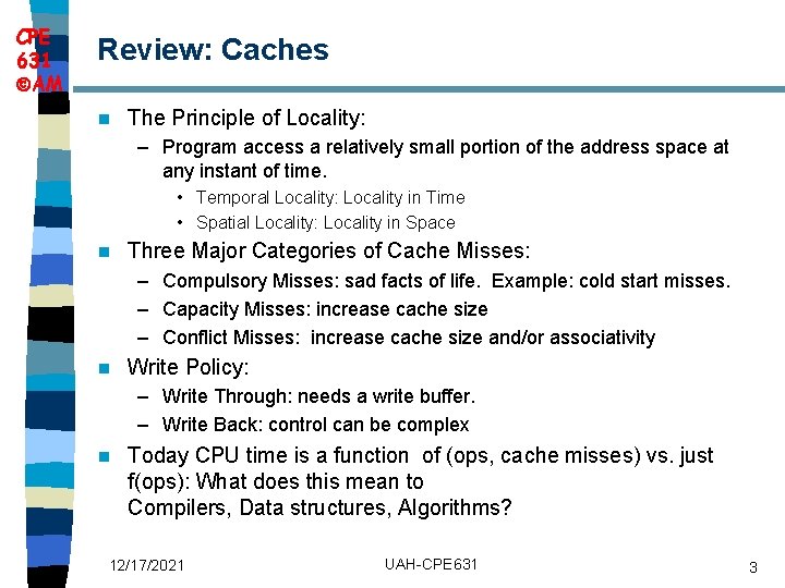
CPE 631 AM Review: Caches n The Principle of Locality: – Program access a relatively small portion of the address space at any instant of time. • Temporal Locality: Locality in Time • Spatial Locality: Locality in Space n Three Major Categories of Cache Misses: – Compulsory Misses: sad facts of life. Example: cold start misses. – Capacity Misses: increase cache size – Conflict Misses: increase cache size and/or associativity n Write Policy: – Write Through: needs a write buffer. – Write Back: control can be complex n Today CPU time is a function of (ops, cache misses) vs. just f(ops): What does this mean to Compilers, Data structures, Algorithms? 12/17/2021 UAH-CPE 631 3

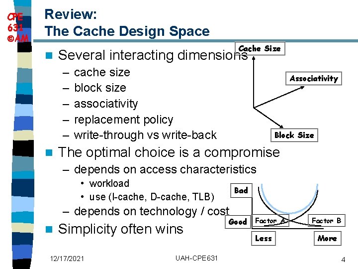
CPE 631 AM Review: The Cache Design Space n Cache Size Several interacting dimensions – – – n cache size block size associativity replacement policy write-through vs write-back Associativity Block Size The optimal choice is a compromise – depends on access characteristics • workload • use (I-cache, D-cache, TLB) Bad – depends on technology / cost n Simplicity often wins 12/17/2021 UAH-CPE 631 Good Factor A Less Factor B More 4

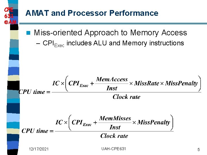
CPE 631 AM AMAT and Processor Performance n Miss-oriented Approach to Memory Access – CPIExec includes ALU and Memory instructions 12/17/2021 UAH-CPE 631 5

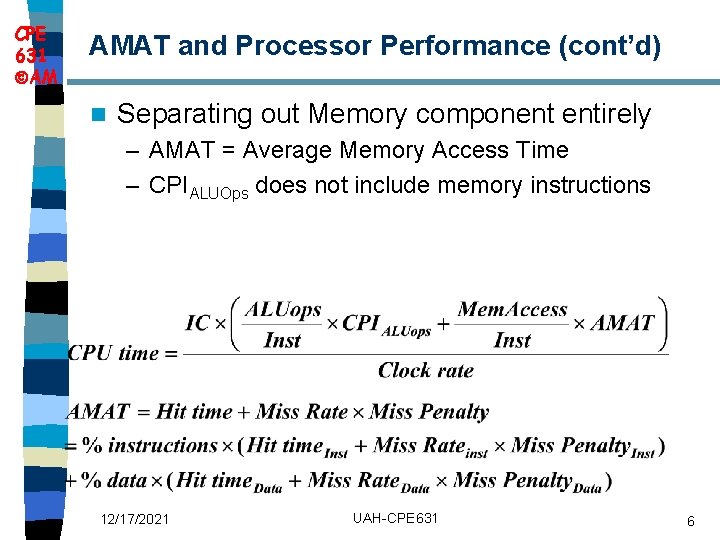
CPE 631 AM AMAT and Processor Performance (cont’d) n Separating out Memory component entirely – AMAT = Average Memory Access Time – CPIALUOps does not include memory instructions 12/17/2021 UAH-CPE 631 6

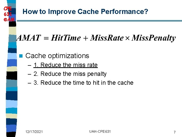
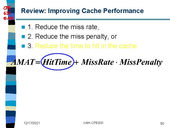
CPE 631 AM How to Improve Cache Performance? n Cache optimizations – 1. Reduce the miss rate – 2. Reduce the miss penalty – 3. Reduce the time to hit in the cache 12/17/2021 UAH-CPE 631 7

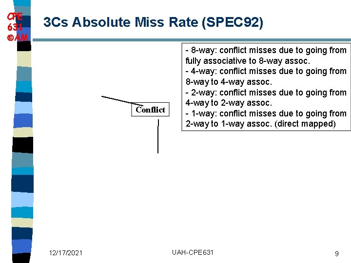
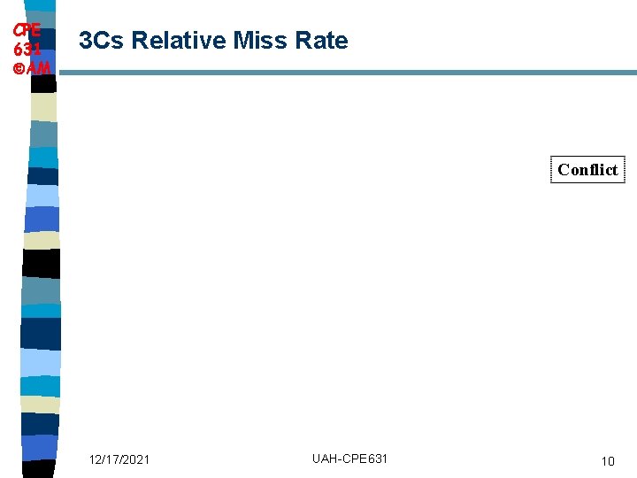
CPE 631 AM Where Misses Come From? n Classifying Misses: 3 Cs – Compulsory — The first access to a block is not in the cache, so the block must be brought into the cache. Also called cold start misses or first reference misses. (Misses in even an Infinite Cache) – Capacity — If the cache cannot contain all the blocks needed during execution of a program, capacity misses will occur due to blocks being discarded and later retrieved. (Misses in Fully Associative Size X Cache) – Conflict — If block-placement strategy is set associative or direct mapped, conflict misses (in addition to compulsory & capacity misses) will occur because a block can be discarded and later retrieved if too many blocks map to its set. Also called collision misses or interference misses. (Misses in N-way Associative, Size X Cache) n More recent, 4 th “C”: – Coherence — Misses caused by cache coherence. 12/17/2021 UAH-CPE 631 8

CPE 631 AM 3 Cs Absolute Miss Rate (SPEC 92) Conflict 12/17/2021 - 8 -way: conflict misses due to going from fully associative to 8 -way assoc. - 4 -way: conflict misses due to going from 8 -way to 4 -way assoc. - 2 -way: conflict misses due to going from 4 -way to 2 -way assoc. - 1 -way: conflict misses due to going from 2 -way to 1 -way assoc. (direct mapped) UAH-CPE 631 9

CPE 631 AM 3 Cs Relative Miss Rate Conflict 12/17/2021 UAH-CPE 631 10

CPE 631 AM Cache Organization? n n 1) 2) 3) 4) 5) n Assume total cache size not changed What happens if: Change Block Size Change Cache Internal Organization Change Associativity Change Compiler Which of 3 Cs is obviously affected? 12/17/2021 UAH-CPE 631 11

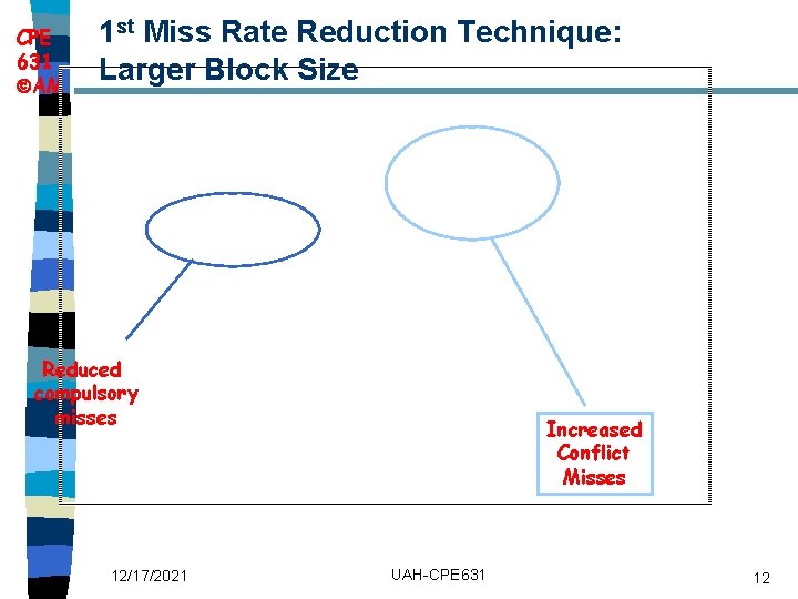
CPE 631 AM 1 st Miss Rate Reduction Technique: Larger Block Size Reduced compulsory misses 12/17/2021 Increased Conflict Misses UAH-CPE 631 12

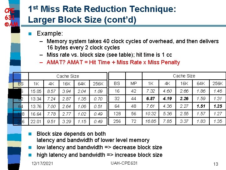
1 st Miss Rate Reduction Technique: Larger Block Size (cont’d) CPE 631 AM n Example: – Memory system takes 40 clock cycles of overhead, and then delivers 16 bytes every 2 clock cycles – Miss rate vs. block size (see table); hit time is 1 cc – AMAT? AMAT = Hit Time + Miss Rate x Miss Penalty Cache Size BS 1 K 4 K 16 K 64 K 256 K BS MP 1 K 4 K 16 K 64 K 256 K 16 15. 05 8. 57 3. 94 2. 04 1. 09 16 42 7. 32 4. 60 2. 66 1. 86 1. 46 32 13. 34 7. 24 2. 87 1. 35 0. 70 32 44 6. 87 4. 19 2. 26 1. 59 1. 31 64 13. 76 7. 00 2. 64 1. 06 0. 51 64 48 7. 61 4. 36 2. 27 1. 51 1. 25 128 16. 64 7. 78 2. 77 1. 02 0. 49 128 56 10. 32 5. 36 2. 55 1. 57 1. 27 256 22. 01 9. 51 3. 29 1. 15 0. 49 256 72 16. 85 7. 85 3. 37 1. 83 1. 35 Block size depends on both latency and bandwidth of lower level memory n low latency and bandwidth => decrease block size n high latency and bandwidth => increase block size n 12/17/2021 UAH-CPE 631 13

CPE 631 AM 2 nd Miss Rate Reduction Technique: Larger Caches n Reduce Capacity misses n Drawbacks: Higher cost, Longer hit time 12/17/2021 UAH-CPE 631 14

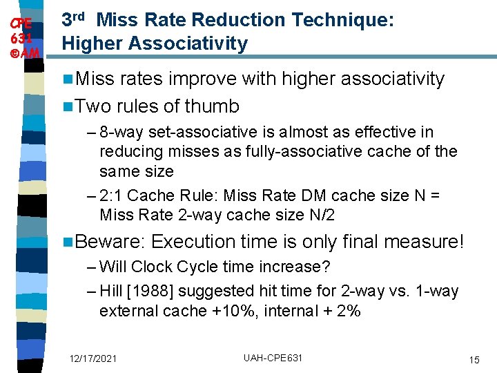
CPE 631 AM 3 rd Miss Rate Reduction Technique: Higher Associativity n Miss rates improve with higher associativity n Two rules of thumb – 8 -way set-associative is almost as effective in reducing misses as fully-associative cache of the same size – 2: 1 Cache Rule: Miss Rate DM cache size N = Miss Rate 2 -way cache size N/2 n Beware: Execution time is only final measure! – Will Clock Cycle time increase? – Hill [1988] suggested hit time for 2 -way vs. 1 -way external cache +10%, internal + 2% 12/17/2021 UAH-CPE 631 15

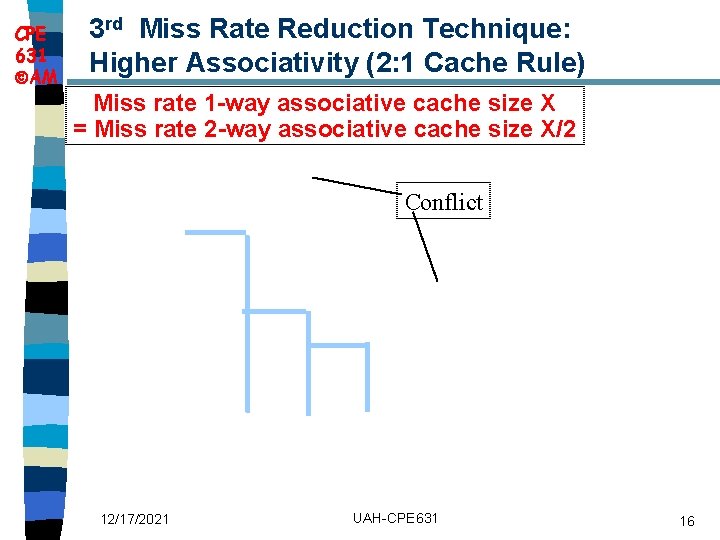
CPE 631 AM 3 rd Miss Rate Reduction Technique: Higher Associativity (2: 1 Cache Rule) Miss rate 1 -way associative cache size X = Miss rate 2 -way associative cache size X/2 Conflict 12/17/2021 UAH-CPE 631 16

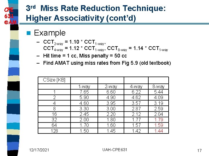
CPE 631 AM 3 rd Miss Rate Reduction Technique: Higher Associativity (cont’d) n Example – CCT 2 -way = 1. 10 * CCT 1 -way, CCT 4 -way = 1. 12 * CCT 1 -way, CCT 8 -way = 1. 14 * CCT 1 -way – Hit time = 1 cc, Miss penalty = 50 cc – Find AMAT using miss rates from Fig 5. 9 (old textbook) CSize [KB] 1 2 4 8 16 32 64 128 12/17/2021 1 -way 7. 65 5. 90 4. 60 3. 30 2. 45 2. 00 1. 70 1. 50 2 -way 6. 60 4. 90 3. 95 3. 00 2. 20 1. 80 1. 60 1. 45 UAH-CPE 631 4 -way 6. 22 4. 62 3. 57 2. 87 2. 12 1. 77 1. 57 1. 42 8 -way 5. 44 4. 09 3. 19 2. 59 2. 04 1. 79 1. 59 1. 44 17

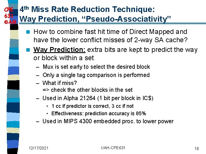
CPE 631 AM 4 th Miss Rate Reduction Technique: Way Prediction, “Pseudo-Associativity” How to combine fast hit time of Direct Mapped and have the lower conflict misses of 2 -way SA cache? n Way Prediction: extra bits are kept to predict the way or block within a set n – Mux is set early to select the desired block – Only a single tag comparison is performed – What if miss? => check the other blocks in the set – Used in Alpha 21264 (1 bit per block in IC$) • 1 cc if predictor is correct, 3 cc if not • Effectiveness: prediction accuracy is 85% – Used in MIPS 4300 embedded proc. to lower power 12/17/2021 UAH-CPE 631 18

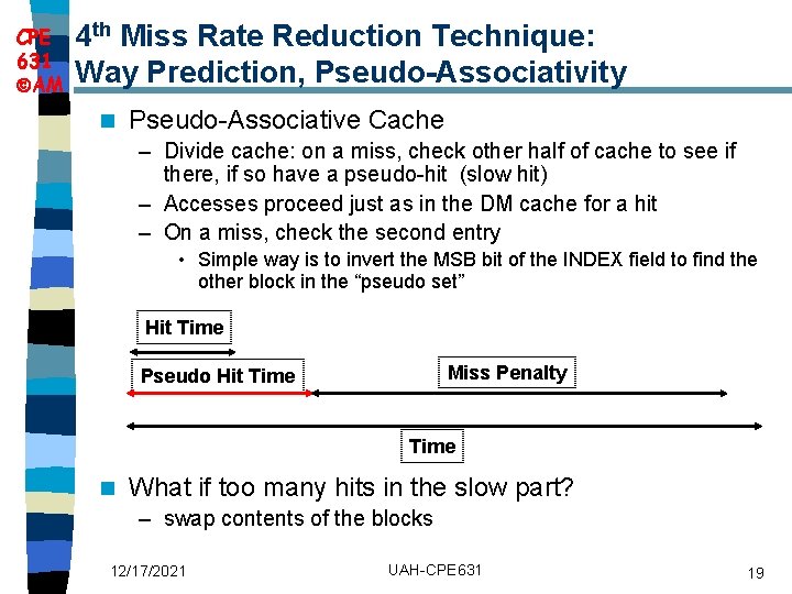
CPE 631 AM 4 th Miss Rate Reduction Technique: Way Prediction, Pseudo-Associativity n Pseudo-Associative Cache – Divide cache: on a miss, check other half of cache to see if there, if so have a pseudo-hit (slow hit) – Accesses proceed just as in the DM cache for a hit – On a miss, check the second entry • Simple way is to invert the MSB bit of the INDEX field to find the other block in the “pseudo set” Hit Time Miss Penalty Pseudo Hit Time n What if too many hits in the slow part? – swap contents of the blocks 12/17/2021 UAH-CPE 631 19

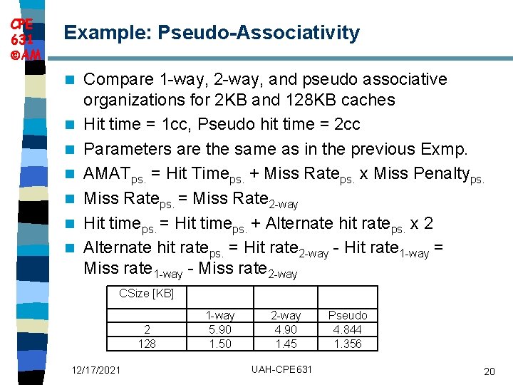
CPE 631 AM Example: Pseudo-Associativity n n n n Compare 1 -way, 2 -way, and pseudo associative organizations for 2 KB and 128 KB caches Hit time = 1 cc, Pseudo hit time = 2 cc Parameters are the same as in the previous Exmp. AMATps. = Hit Timeps. + Miss Rateps. x Miss Penaltyps. Miss Rateps. = Miss Rate 2 -way Hit timeps. = Hit timeps. + Alternate hit rateps. x 2 Alternate hit rateps. = Hit rate 2 -way - Hit rate 1 -way = Miss rate 1 -way - Miss rate 2 -way CSize [KB] 2 128 12/17/2021 1 -way 5. 90 1. 50 2 -way 4. 90 1. 45 UAH-CPE 631 Pseudo 4. 844 1. 356 20

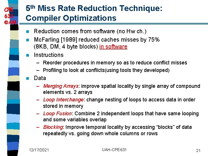
CPE 631 AM 5 th Miss Rate Reduction Technique: Compiler Optimizations Reduction comes from software (no Hw ch. ) n Mc. Farling [1989] reduced caches misses by 75% (8 KB, DM, 4 byte blocks) in software n Instructions n – Reorder procedures in memory so as to reduce conflict misses – Profiling to look at conflicts(using tools they developed) n Data – Merging Arrays: improve spatial locality by single array of compound elements vs. 2 arrays – Loop Interchange: change nesting of loops to access data in order stored in memory – Loop Fusion: Combine 2 independent loops that have same looping and some variables overlap – Blocking: Improve temporal locality by accessing “blocks” of data repeatedly vs. going down whole columns or rows 12/17/2021 UAH-CPE 631 21

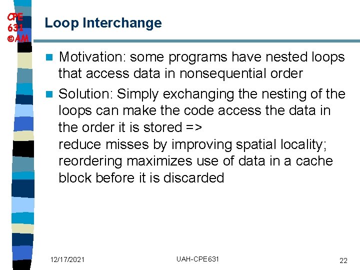
CPE 631 AM Loop Interchange Motivation: some programs have nested loops that access data in nonsequential order n Solution: Simply exchanging the nesting of the loops can make the code access the data in the order it is stored => reduce misses by improving spatial locality; reordering maximizes use of data in a cache block before it is discarded n 12/17/2021 UAH-CPE 631 22

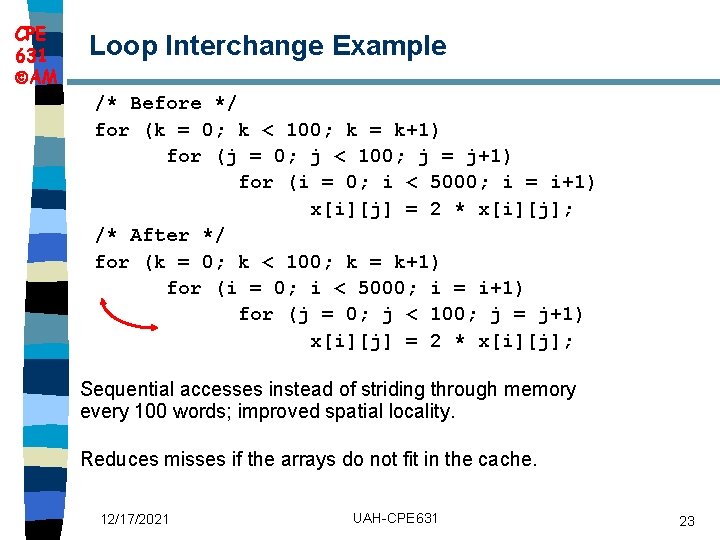
CPE 631 AM Loop Interchange Example /* Before */ for (k = 0; k < 100; k = k+1) for (j = 0; j < 100; j = j+1) for (i = 0; i < 5000; i = i+1) x[i][j] = 2 * x[i][j]; /* After */ for (k = 0; k < 100; k = k+1) for (i = 0; i < 5000; i = i+1) for (j = 0; j < 100; j = j+1) x[i][j] = 2 * x[i][j]; Sequential accesses instead of striding through memory every 100 words; improved spatial locality. Reduces misses if the arrays do not fit in the cache. 12/17/2021 UAH-CPE 631 23

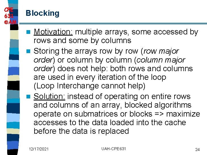
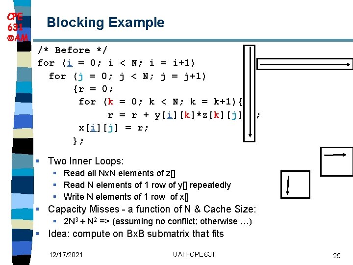
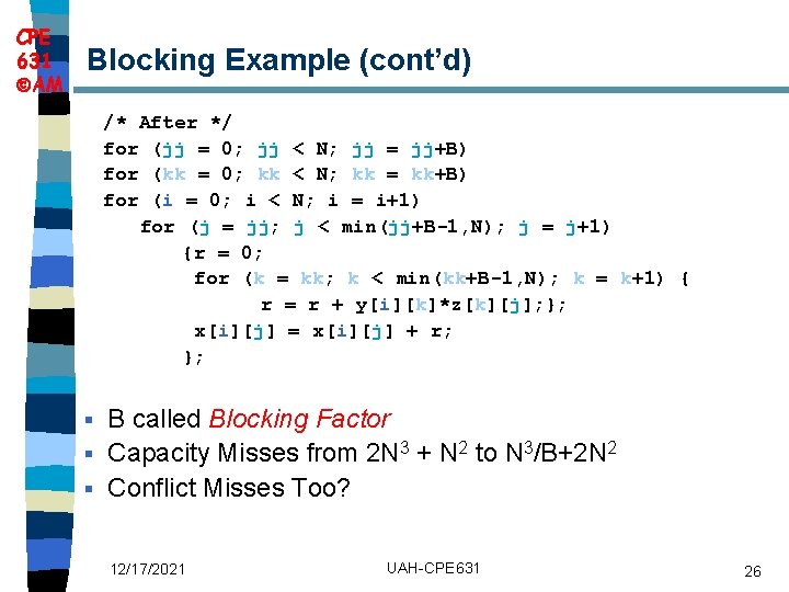
CPE 631 AM Blocking Motivation: multiple arrays, some accessed by rows and some by columns n Storing the arrays row by row (row major order) or column by column (column major order) does not help: both rows and columns are used in every iteration of the loop (Loop Interchange cannot help) n Solution: instead of operating on entire rows and columns of an array, blocked algorithms operate on submatrices or blocks => maximize accesses to the data loaded into the cache before the data is replaced n 12/17/2021 UAH-CPE 631 24

CPE 631 AM Blocking Example /* Before */ for (i = 0; i < N; i = i+1) for (j = 0; j < N; j = j+1) {r = 0; for (k = 0; k < N; k = k+1){ r = r + y[i][k]*z[k][j]; }; x[i][j] = r; }; § Two Inner Loops: § Read all Nx. N elements of z[] § Read N elements of 1 row of y[] repeatedly § Write N elements of 1 row of x[] § Capacity Misses - a function of N & Cache Size: § 2 N 3 + N 2 => (assuming no conflict; otherwise …) § Idea: compute on Bx. B submatrix that fits 12/17/2021 UAH-CPE 631 25

CPE 631 AM Blocking Example (cont’d) /* After */ for (jj = 0; jj < N; jj = jj+B) for (kk = 0; kk < N; kk = kk+B) for (i = 0; i < N; i = i+1) for (j = jj; j < min(jj+B-1, N); j = j+1) {r = 0; for (k = kk; k < min(kk+B-1, N); k = k+1) { r = r + y[i][k]*z[k][j]; }; x[i][j] = x[i][j] + r; }; B called Blocking Factor § Capacity Misses from 2 N 3 + N 2 to N 3/B+2 N 2 § Conflict Misses Too? § 12/17/2021 UAH-CPE 631 26

CPE 631 AM Merging Arrays Motivation: some programs reference multiple arrays in the same dimension with the same indices at the same time => these accesses can interfere with each other, leading to conflict misses n Solution: combine these independent matrices into a single compound array, so that a single cache block can contain the desired elements n 12/17/2021 UAH-CPE 631 27
![CPE 631 AM Merging Arrays Example Before 2 sequential arrays int valSIZE CPE 631 AM Merging Arrays Example /* Before: 2 sequential arrays */ int val[SIZE];](https://slidetodoc.com/presentation_image_h2/14e267ef5c3e5ecfb19bc4e59d1fd70a/image-28.jpg)
CPE 631 AM Merging Arrays Example /* Before: 2 sequential arrays */ int val[SIZE]; int key[SIZE]; /* After: 1 array of stuctures */ struct merge { int val; int key; }; struct merged_array[SIZE]; 12/17/2021 UAH-CPE 631 28

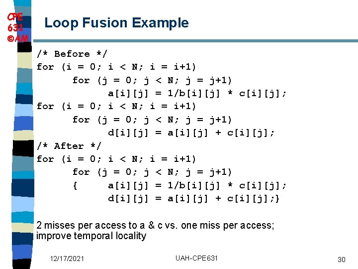
CPE 631 AM Loop Fusion Some programs have separate sections of code that access with the same loops, performing different computations on the common data n Solution: “Fuse” the code into a single loop => the data that are fetched into the cache can be used repeatedly before being swapped out => reducing misses via improved temporal locality n 12/17/2021 UAH-CPE 631 29

CPE 631 AM Loop Fusion Example /* Before */ for (i = 0; i < N; i = i+1) for (j = 0; j < N; j = j+1) a[i][j] = 1/b[i][j] * c[i][j]; for (i = 0; i < N; i = i+1) for (j = 0; j < N; j = j+1) d[i][j] = a[i][j] + c[i][j]; /* After */ for (i = 0; i < N; i = i+1) for (j = 0; j < N; j = j+1) { a[i][j] = 1/b[i][j] * c[i][j]; d[i][j] = a[i][j] + c[i][j]; } 2 misses per access to a & c vs. one miss per access; improve temporal locality 12/17/2021 UAH-CPE 631 30

CPE 631 AM Summary of Compiler Optimizations to Reduce Cache Misses (by hand) 12/17/2021 UAH-CPE 631 31

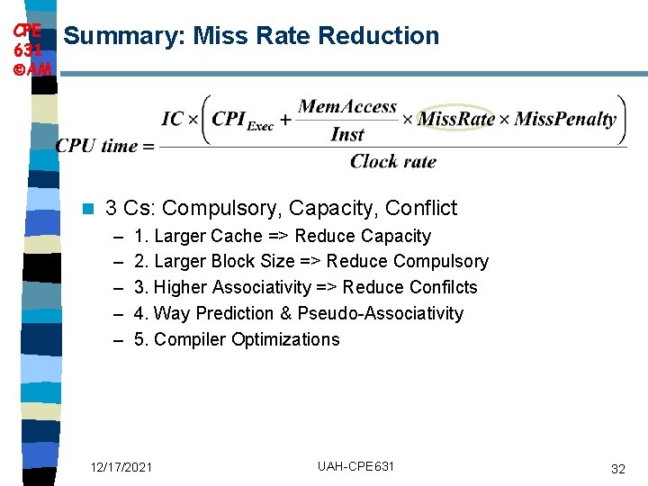
CPE 631 AM Summary: Miss Rate Reduction n 3 Cs: Compulsory, Capacity, Conflict – – – 1. Larger Cache => Reduce Capacity 2. Larger Block Size => Reduce Compulsory 3. Higher Associativity => Reduce Confilcts 4. Way Prediction & Pseudo-Associativity 5. Compiler Optimizations 12/17/2021 UAH-CPE 631 32

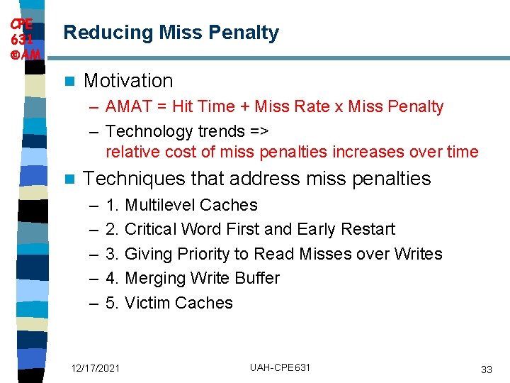
CPE 631 AM Reducing Miss Penalty n Motivation – AMAT = Hit Time + Miss Rate x Miss Penalty – Technology trends => relative cost of miss penalties increases over time n Techniques that address miss penalties – – – 1. Multilevel Caches 2. Critical Word First and Early Restart 3. Giving Priority to Read Misses over Writes 4. Merging Write Buffer 5. Victim Caches 12/17/2021 UAH-CPE 631 33

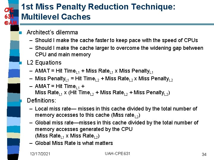
CPE 631 AM 1 st Miss Penalty Reduction Technique: Multilevel Caches n Architect’s dilemma – Should I make the cache faster to keep pace with the speed of CPUs – Should I make the cache larger to overcome the widening gap between CPU and main memory n L 2 Equations – AMAT = Hit Time. L 1 + Miss Rate. L 1 x Miss Penalty. L 1 – Miss Penalty. L 1 = Hit Time. L 2 + Miss Rate. L 2 x Miss Penalty. L 2 – AMAT = Hit Time. L 1 + Miss Rate. L 1 x (Hit Time. L 2 + Miss Rate. L 2 + Miss Penalty. L 2) n Definitions: – Local miss rate— misses in this cache divided by the total number of memory accesses to this cache (Miss rate. L 2) – Global miss rate—misses in this cache divided by the total number of memory accesses generated by the CPU (Miss Rate. L 1 x Miss Rate. L 2) – Global Miss Rate is what matters 12/17/2021 UAH-CPE 631 34

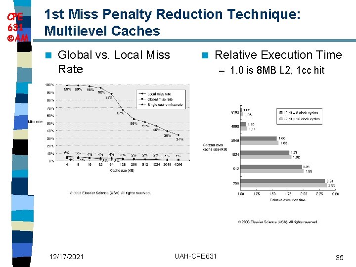
CPE 631 AM 1 st Miss Penalty Reduction Technique: Multilevel Caches n Global vs. Local Miss Rate 12/17/2021 n Relative Execution Time – 1. 0 is 8 MB L 2, 1 cc hit UAH-CPE 631 35

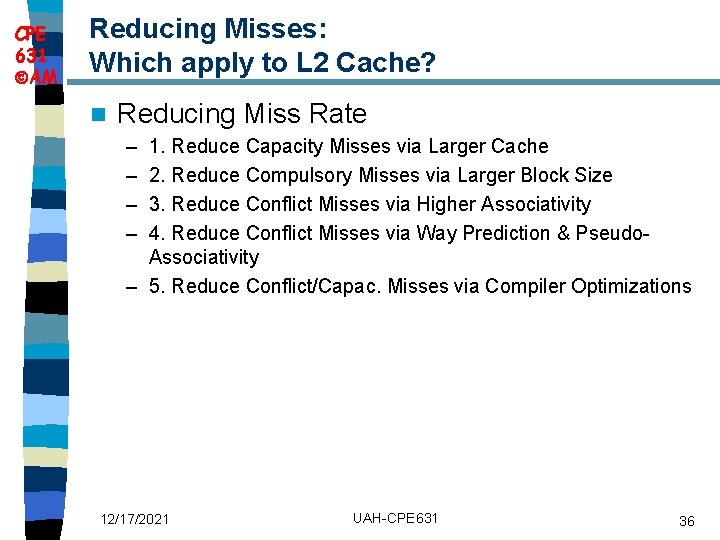
CPE 631 AM Reducing Misses: Which apply to L 2 Cache? n Reducing Miss Rate – – 1. Reduce Capacity Misses via Larger Cache 2. Reduce Compulsory Misses via Larger Block Size 3. Reduce Conflict Misses via Higher Associativity 4. Reduce Conflict Misses via Way Prediction & Pseudo. Associativity – 5. Reduce Conflict/Capac. Misses via Compiler Optimizations 12/17/2021 UAH-CPE 631 36

CPE 631 AM L 2 cache block size & A. M. A. T. n 32 KB L 1, 8 byte path to memory 12/17/2021 UAH-CPE 631 37

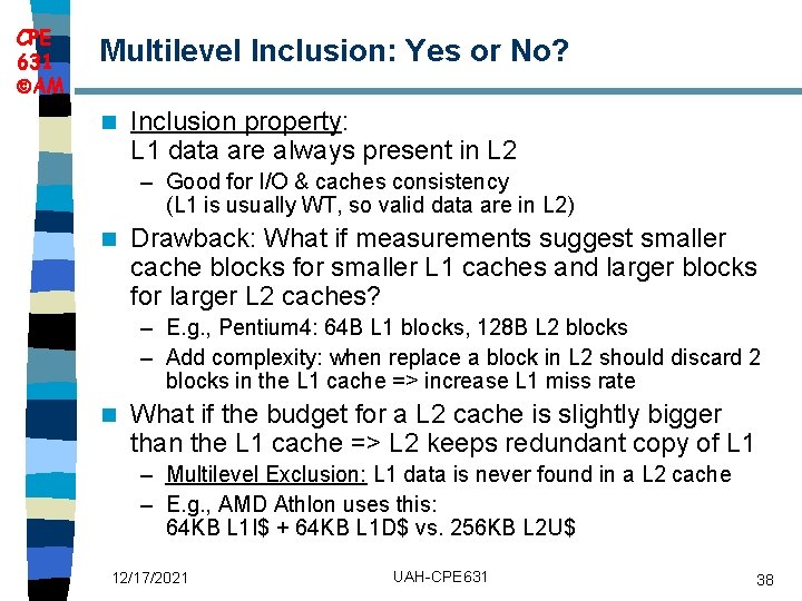
CPE 631 AM Multilevel Inclusion: Yes or No? n Inclusion property: L 1 data are always present in L 2 – Good for I/O & caches consistency (L 1 is usually WT, so valid data are in L 2) n Drawback: What if measurements suggest smaller cache blocks for smaller L 1 caches and larger blocks for larger L 2 caches? – E. g. , Pentium 4: 64 B L 1 blocks, 128 B L 2 blocks – Add complexity: when replace a block in L 2 should discard 2 blocks in the L 1 cache => increase L 1 miss rate n What if the budget for a L 2 cache is slightly bigger than the L 1 cache => L 2 keeps redundant copy of L 1 – Multilevel Exclusion: L 1 data is never found in a L 2 cache – E. g. , AMD Athlon uses this: 64 KB L 1 I$ + 64 KB L 1 D$ vs. 256 KB L 2 U$ 12/17/2021 UAH-CPE 631 38

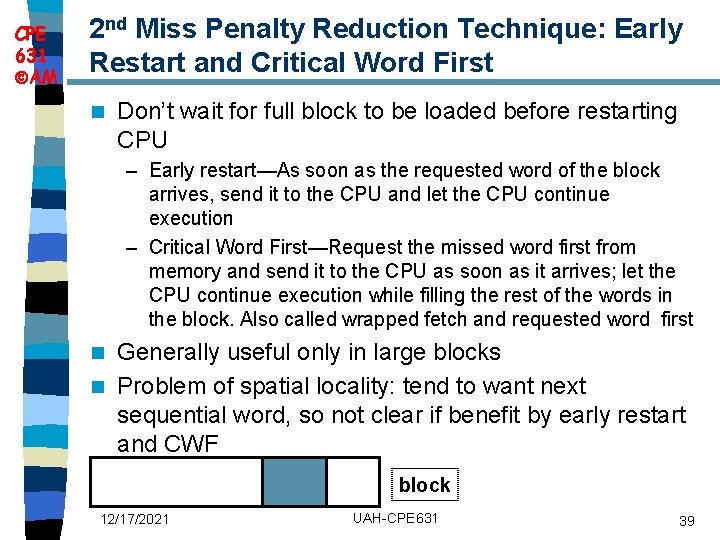
CPE 631 AM 2 nd Miss Penalty Reduction Technique: Early Restart and Critical Word First n Don’t wait for full block to be loaded before restarting CPU – Early restart—As soon as the requested word of the block arrives, send it to the CPU and let the CPU continue execution – Critical Word First—Request the missed word first from memory and send it to the CPU as soon as it arrives; let the CPU continue execution while filling the rest of the words in the block. Also called wrapped fetch and requested word first Generally useful only in large blocks n Problem of spatial locality: tend to want next sequential word, so not clear if benefit by early restart and CWF n block 12/17/2021 UAH-CPE 631 39

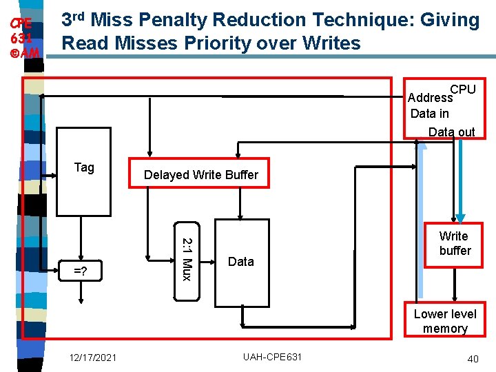
CPE 631 AM 3 rd Miss Penalty Reduction Technique: Giving Read Misses Priority over Writes CPU Address Data in Data out Tag 2: 1 Mux =? Delayed Write Buffer Data Write buffer Lower level memory 12/17/2021 UAH-CPE 631 40

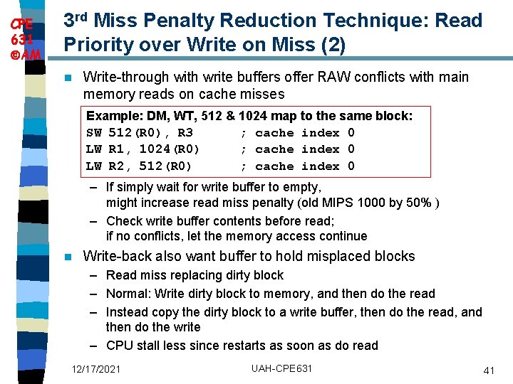
CPE 631 AM 3 rd Miss Penalty Reduction Technique: Read Priority over Write on Miss (2) n Write-through with write buffers offer RAW conflicts with main memory reads on cache misses Example: DM, WT, 512 & 1024 map to the same block: SW 512(R 0), R 3 ; cache index 0 LW R 1, 1024(R 0) ; cache index 0 LW R 2, 512(R 0) ; cache index 0 – If simply wait for write buffer to empty, might increase read miss penalty (old MIPS 1000 by 50% ) – Check write buffer contents before read; if no conflicts, let the memory access continue n Write-back also want buffer to hold misplaced blocks – Read miss replacing dirty block – Normal: Write dirty block to memory, and then do the read – Instead copy the dirty block to a write buffer, then do the read, and then do the write – CPU stall less since restarts as soon as do read 12/17/2021 UAH-CPE 631 41

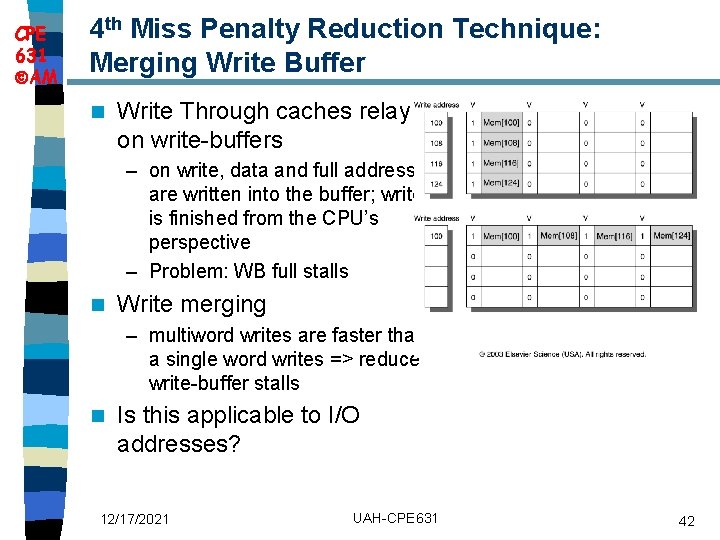
CPE 631 AM 4 th Miss Penalty Reduction Technique: Merging Write Buffer n Write Through caches relay on write-buffers – on write, data and full address are written into the buffer; write is finished from the CPU’s perspective – Problem: WB full stalls n Write merging – multiword writes are faster than a single word writes => reduce write-buffer stalls n Is this applicable to I/O addresses? 12/17/2021 UAH-CPE 631 42

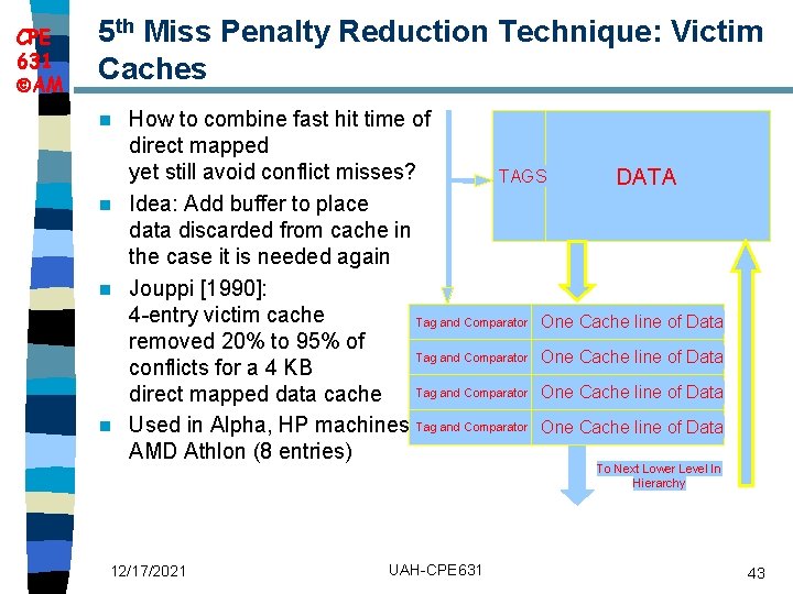
CPE 631 AM 5 th Miss Penalty Reduction Technique: Victim Caches How to combine fast hit time of direct mapped yet still avoid conflict misses? TAGS DATA n Idea: Add buffer to place data discarded from cache in the case it is needed again n Jouppi [1990]: 4 -entry victim cache Tag and Comparator One Cache line of Data removed 20% to 95% of Tag and Comparator One Cache line of Data conflicts for a 4 KB Tag and Comparator One Cache line of Data direct mapped data cache n Used in Alpha, HP machines, Tag and Comparator One Cache line of Data AMD Athlon (8 entries) n To Next Lower Level In Hierarchy 12/17/2021 UAH-CPE 631 43

CPE 631 AM Summary of Miss Penalty Reducing Tec. n n n 1. Multilevel Caches 2. Critical Word First and Early Restart 3. Giving Priority to Read Misses over Writes 4. Merging Write Buffer 5. Victim Caches 12/17/2021 UAH-CPE 631 44

CPE 631 AM Reducing Cache Miss Penalty or Miss Rate via Parallelism Idea: overlap the execution of instructions with activity in memory hierarchy n Miss Rate/Penalty reduction techniques n – 1. Nonblocking caches • reduce stalls on cache misses in CPUs with out-of-order completion – 2. Hardware prefetching of instructions and data • reduce miss penalty – 3. Compiler controlled prefetching 12/17/2021 UAH-CPE 631 45

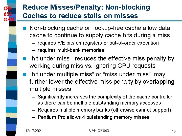
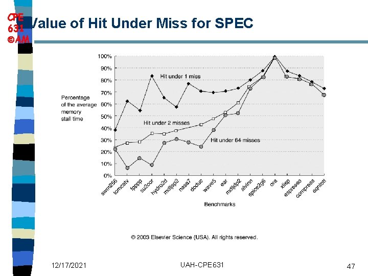
CPE 631 AM Reduce Misses/Penalty: Non-blocking Caches to reduce stalls on misses n Non-blocking cache or lockup-free cache allow data cache to continue to supply cache hits during a miss – requires F/E bits on registers or out-of-order execution – requires multi-bank memories “hit under miss” reduces the effective miss penalty by working during miss vs. ignoring CPU requests n “hit under multiple miss” or “miss under miss” may further lower the effective miss penalty by overlapping multiple misses n – Significantly increases the complexity of the cache controller as there can be multiple outstanding memory accesses – Requires muliple memory banks (otherwise cannot support) – Pentium Pro allows 4 outstanding memory misses 12/17/2021 UAH-CPE 631 46

CPE 631 Value AM of Hit Under Miss for SPEC 12/17/2021 UAH-CPE 631 47

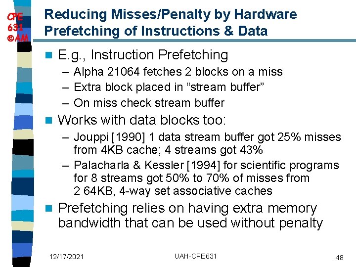
CPE 631 AM Reducing Misses/Penalty by Hardware Prefetching of Instructions & Data n E. g. , Instruction Prefetching – Alpha 21064 fetches 2 blocks on a miss – Extra block placed in “stream buffer” – On miss check stream buffer n Works with data blocks too: – Jouppi [1990] 1 data stream buffer got 25% misses from 4 KB cache; 4 streams got 43% – Palacharla & Kessler [1994] for scientific programs for 8 streams got 50% to 70% of misses from 2 64 KB, 4 -way set associative caches n Prefetching relies on having extra memory bandwidth that can be used without penalty 12/17/2021 UAH-CPE 631 48

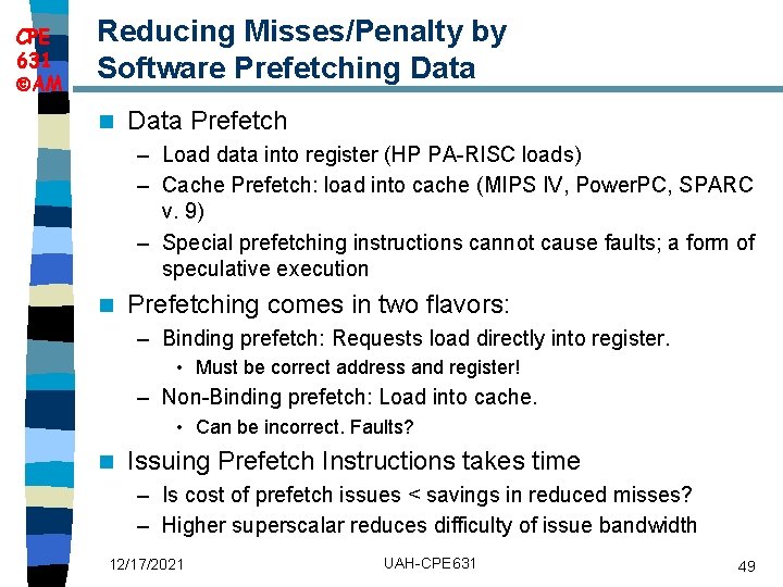
CPE 631 AM Reducing Misses/Penalty by Software Prefetching Data n Data Prefetch – Load data into register (HP PA-RISC loads) – Cache Prefetch: load into cache (MIPS IV, Power. PC, SPARC v. 9) – Special prefetching instructions cannot cause faults; a form of speculative execution n Prefetching comes in two flavors: – Binding prefetch: Requests load directly into register. • Must be correct address and register! – Non-Binding prefetch: Load into cache. • Can be incorrect. Faults? n Issuing Prefetch Instructions takes time – Is cost of prefetch issues < savings in reduced misses? – Higher superscalar reduces difficulty of issue bandwidth 12/17/2021 UAH-CPE 631 49

CPE 631 AM Review: Improving Cache Performance 1. Reduce the miss rate, n 2. Reduce the miss penalty, or n 3. Reduce the time to hit in the cache. n 12/17/2021 UAH-CPE 631 50

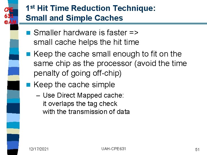
CPE 631 AM 1 st Hit Time Reduction Technique: Small and Simple Caches Smaller hardware is faster => small cache helps the hit time n Keep the cache small enough to fit on the same chip as the processor (avoid the time penalty of going off-chip) n Keep the cache simple n – Use Direct Mapped cache: it overlaps the tag check with the transmission of data 12/17/2021 UAH-CPE 631 51

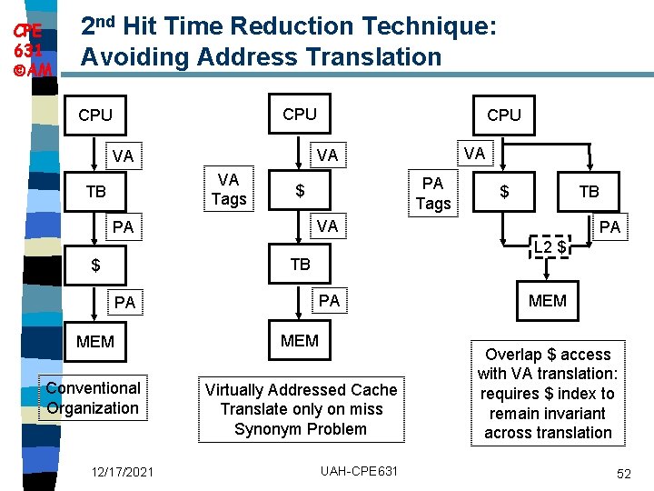
CPE 631 AM 2 nd Hit Time Reduction Technique: Avoiding Address Translation CPU VA Tags PA Tags $ PA MEM Conventional Organization Virtually Addressed Cache Translate only on miss Synonym Problem 12/17/2021 TB PA L 2 $ TB PA $ VA VA VA TB CPU UAH-CPE 631 MEM Overlap $ access with VA translation: requires $ index to remain invariant across translation 52

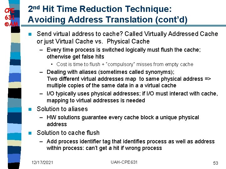
CPE 631 AM 2 nd Hit Time Reduction Technique: Avoiding Address Translation (cont’d) n Send virtual address to cache? Called Virtually Addressed Cache or just Virtual Cache vs. Physical Cache – Every time process is switched logically must flush the cache; otherwise get false hits • Cost is time to flush + “compulsory” misses from empty cache – Dealing with aliases (sometimes called synonyms); Two different virtual addresses map to same physical address => multiple copies of the same data in a a virtual cache – I/O typically uses physical addresses; if I/O must interact with cache, mapping to virtual addresses is needed n Solution to aliases – HW solutions guarantee every cache block a unique physical address n Solution to cache flush – Add process identifier tag that identifies process as well as address within process: can’t get a hit if wrong process 12/17/2021 UAH-CPE 631 53

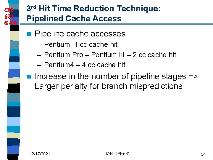
CPE 631 AM 3 rd Hit Time Reduction Technique: Pipelined Cache Access n Pipeline cache accesses – Pentium: 1 cc cache hit – Pentium Pro – Pentium III – 2 cc cache hit – Pentium 4 – 4 cc cache hit n Increase in the number of pipeline stages => Larger penalty for branch mispredictions 12/17/2021 UAH-CPE 631 54

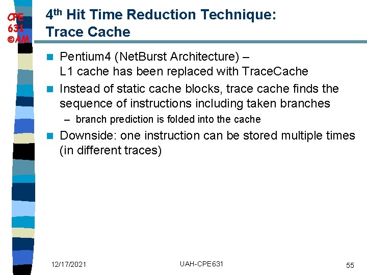
CPE 631 AM 4 th Hit Time Reduction Technique: Trace Cache Pentium 4 (Net. Burst Architecture) – L 1 cache has been replaced with Trace. Cache n Instead of static cache blocks, trace cache finds the sequence of instructions including taken branches n – branch prediction is folded into the cache n Downside: one instruction can be stored multiple times (in different traces) 12/17/2021 UAH-CPE 631 55

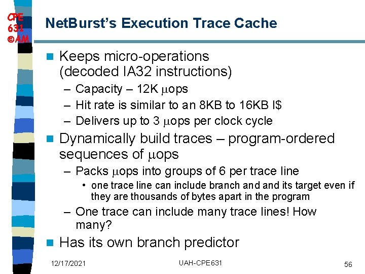
CPE 631 AM Net. Burst’s Execution Trace Cache n Keeps micro-operations (decoded IA 32 instructions) – Capacity – 12 K ops – Hit rate is similar to an 8 KB to 16 KB I$ – Delivers up to 3 ops per clock cycle n Dynamically build traces – program-ordered sequences of ops – Packs ops into groups of 6 per trace line • one trace line can include branch and its target even if they are thousands of bytes apart in the program – One trace can include many trace lines! How many? n Has its own branch predictor 12/17/2021 UAH-CPE 631 56

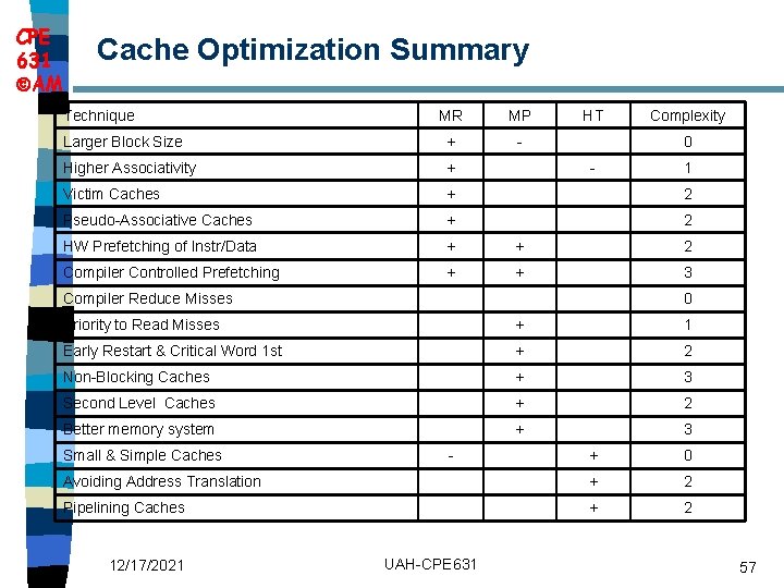
CPE 631 AM Cache Optimization Summary Technique MR MP HT Complexity Larger Block Size + - Higher Associativity + Victim Caches + 2 Pseudo-Associative Caches + 2 HW Prefetching of Instr/Data + + 2 Compiler Controlled Prefetching + + 3 0 - Compiler Reduce Misses 1 0 Priority to Read Misses + 1 Early Restart & Critical Word 1 st + 2 Non-Blocking Caches + 3 Second Level Caches + 2 Better memory system + 3 Small & Simple Caches + 0 Avoiding Address Translation + 2 Pipelining Caches + 2 12/17/2021 - UAH-CPE 631 57

Main Memory

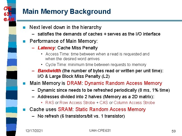
CPE 631 AM Main Memory Background n Next level down in the hierarchy – satisfies the demands of caches + serves as the I/O interface n Performance of Main Memory: – Latency: Cache Miss Penalty • Access Time: time between when a read is requested and when the desired word arrives • Cycle Time: minimum time between requests to memory – Bandwidth (the number of bytes read or written per unit time): I/O & Large Block Miss Penalty (L 2) n Main Memory is DRAM: Dynamic Random Access Memory – Dynamic since needs to be refreshed periodically (8 ms, 1% time) – Addresses divided into 2 halves (Memory as a 2 D matrix): • RAS or Row Access Strobe + CAS or Column Access Strobe n Cache uses SRAM: Static Random Access Memory – No refresh (6 transistors/bit vs. 1 transistor) 12/17/2021 UAH-CPE 631 59

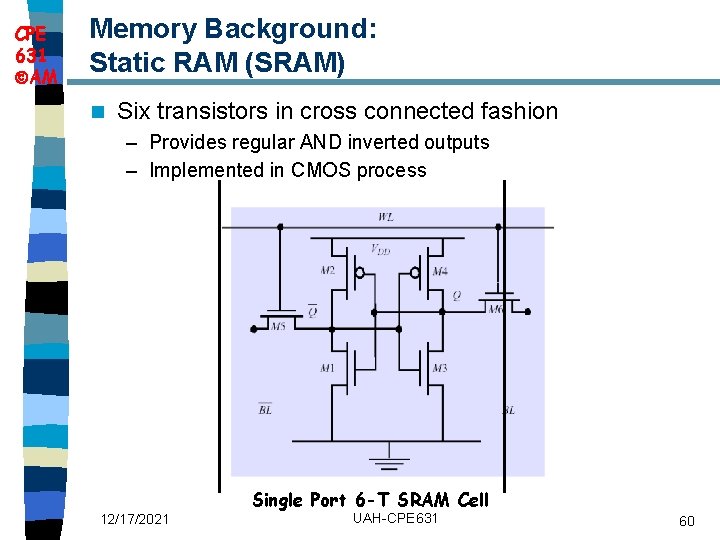
CPE 631 AM Memory Background: Static RAM (SRAM) n Six transistors in cross connected fashion – Provides regular AND inverted outputs – Implemented in CMOS process Single Port 6 -T SRAM Cell 12/17/2021 UAH-CPE 631 60

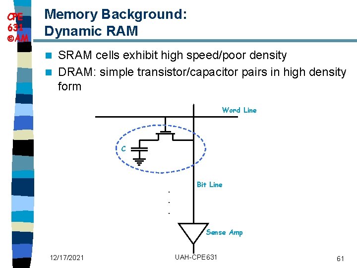
CPE 631 AM Memory Background: Dynamic RAM SRAM cells exhibit high speed/poor density n DRAM: simple transistor/capacitor pairs in high density form n Word Line C . . . Bit Line Sense Amp 12/17/2021 UAH-CPE 631 61

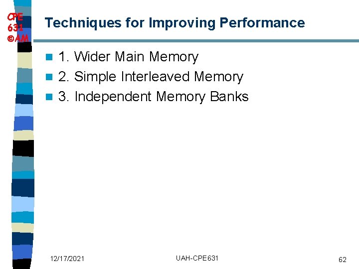
CPE 631 AM Techniques for Improving Performance 1. Wider Main Memory n 2. Simple Interleaved Memory n 3. Independent Memory Banks n 12/17/2021 UAH-CPE 631 62

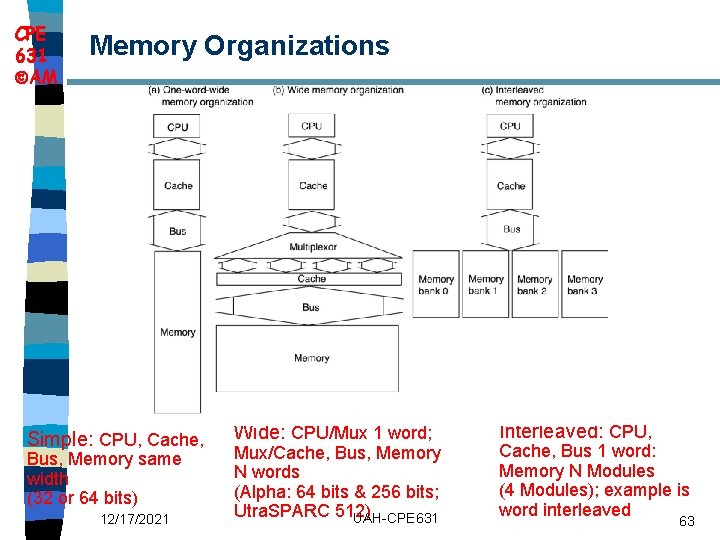
CPE 631 AM Memory Organizations Simple: CPU, Cache, Bus, Memory same width (32 or 64 bits) 12/17/2021 Wide: CPU/Mux 1 word; Mux/Cache, Bus, Memory N words (Alpha: 64 bits & 256 bits; Utra. SPARC 512) UAH-CPE 631 Interleaved: CPU, Cache, Bus 1 word: Memory N Modules (4 Modules); example is word interleaved 63

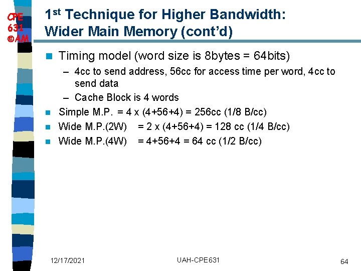
CPE 631 AM 1 st Technique for Higher Bandwidth: Wider Main Memory (cont’d) n Timing model (word size is 8 bytes = 64 bits) – 4 cc to send address, 56 cc for access time per word, 4 cc to send data – Cache Block is 4 words n Simple M. P. = 4 x (4+56+4) = 256 cc (1/8 B/cc) n Wide M. P. (2 W) = 2 x (4+56+4) = 128 cc (1/4 B/cc) n Wide M. P. (4 W) = 4+56+4 = 64 cc (1/2 B/cc) 12/17/2021 UAH-CPE 631 64

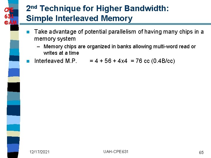
CPE 631 AM 2 nd Technique for Higher Bandwidth: Simple Interleaved Memory n Take advantage of potential parallelism of having many chips in a memory system – Memory chips are organized in banks allowing multi-word read or writes at a time n Interleaved M. P. 12/17/2021 = 4 + 56 + 4 x 4 = 76 cc (0. 4 B/cc) UAH-CPE 631 65

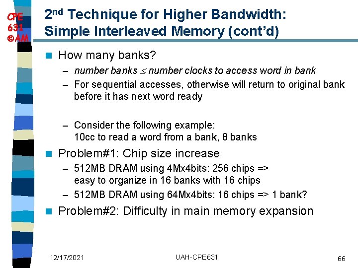
CPE 631 AM 2 nd Technique for Higher Bandwidth: Simple Interleaved Memory (cont’d) n How many banks? – number banks number clocks to access word in bank – For sequential accesses, otherwise will return to original bank before it has next word ready – Consider the following example: 10 cc to read a word from a bank, 8 banks n Problem#1: Chip size increase – 512 MB DRAM using 4 Mx 4 bits: 256 chips => easy to organize in 16 banks with 16 chips – 512 MB DRAM using 64 Mx 4 bits: 16 chips => 1 bank? n Problem#2: Difficulty in main memory expansion 12/17/2021 UAH-CPE 631 66

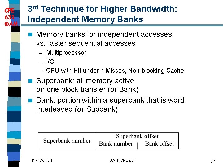
CPE 631 AM 3 rd Technique for Higher Bandwidth: Independent Memory Banks n Memory banks for independent accesses vs. faster sequential accesses – Multiprocessor – I/O – CPU with Hit under n Misses, Non-blocking Cache Superbank: all memory active on one block transfer (or Bank) n Bank: portion within a superbank that is word interleaved (or Subbank) n 12/17/2021 UAH-CPE 631 67
![CPE 631 AM Avoiding Bank Conflicts int x256512 Lots of banks for j CPE 631 AM Avoiding Bank Conflicts int x[256][512]; Lots of banks for (j =](https://slidetodoc.com/presentation_image_h2/14e267ef5c3e5ecfb19bc4e59d1fd70a/image-68.jpg)
CPE 631 AM Avoiding Bank Conflicts int x[256][512]; Lots of banks for (j = 0; j < 512; j = j+1) n Even with 128 banks, for (i = 0; i < 256; i = i+1) since 512 is multiple of 128, x[i][j] = 2 * x[i][j]; conflict on word accesses n SW: loop interchange or declaring array not power of 2 (“array padding”) n HW: Prime number of banks – bank number = address mod number of banks – address within bank = address / number of words in bank – modulo & divide per memory access with prime no. banks? – address within bank = address mod number words in bank – bank number? easy if 2 N words per bank n 12/17/2021 UAH-CPE 631 68

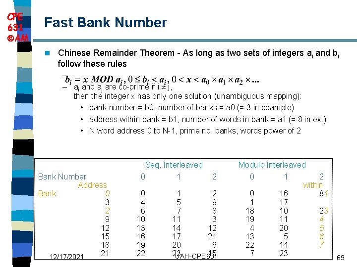
CPE 631 AM Fast Bank Number n Chinese Remainder Theorem - As long as two sets of integers ai and bi follow these rules – – ai and aj are co-prime if i j, then the integer x has only one solution (unambiguous mapping): • bank number = b 0, number of banks = a 0 (= 3 in example) • address within bank = b 1, number of words in bank = a 1 (= 8 in ex. ) • N word address 0 to N-1, prime no. banks, words power of 2 Bank Number: Address Bank: 0 3 2 9 12 15 18 21 12/17/2021 Seq. Interleaved 0 1 0 4 6 10 13 16 19 22 2 1 2 5 9 7 8 11 3 14 12 17 21 20 6 23 15 UAH-CPE 631 Modulo Interleaved 0 1 2 within 0 16 81 1 17 18 10 23 19 11 4 4 20 5 13 5 6 22 14 7 7 23 69

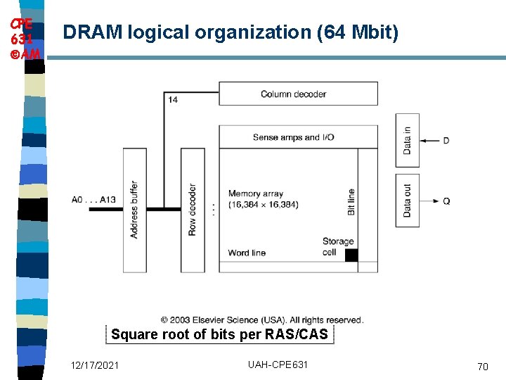
CPE 631 AM DRAM logical organization (64 Mbit) Square root of bits per RAS/CAS 12/17/2021 UAH-CPE 631 70

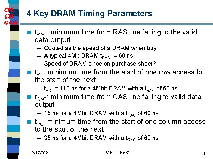
CPE 631 AM 4 Key DRAM Timing Parameters n t. RAC: minimum time from RAS line falling to the valid data output – Quoted as the speed of a DRAM when buy – A typical 4 Mb DRAM t. RAC = 60 ns – Speed of DRAM since on purchase sheet? n t. RC: minimum time from the start of one row access to the start of the next – t. RC = 110 ns for a 4 Mbit DRAM with a t. RAC of 60 ns n t. CAC: minimum time from CAS line falling to valid data output – 15 ns for a 4 Mbit DRAM with a t. RAC of 60 ns n t. PC: minimum time from the start of one column access to the start of the next – 35 ns for a 4 Mbit DRAM with a t. RAC of 60 ns 12/17/2021 UAH-CPE 631 71

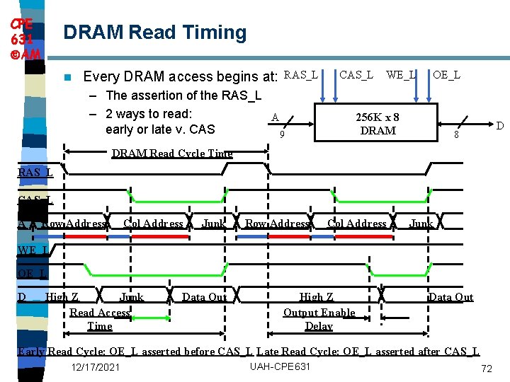
CPE 631 AM DRAM Read Timing n Every DRAM access begins at: RAS_L CAS_L – The assertion of the RAS_L – 2 ways to read: A early or late v. CAS 9 WE_L OE_L 256 K x 8 DRAM D 8 DRAM Read Cycle Time RAS_L CAS_L A Row Address Col Address Junk WE_L OE_L D High Z Junk Read Access Time Data Out High Z Output Enable Delay Data Out Early Read Cycle: OE_L asserted before CAS_L Late Read Cycle: OE_L asserted after CAS_L 12/17/2021 UAH-CPE 631 72

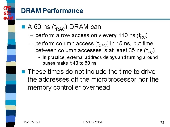
CPE 631 AM DRAM Performance n A 60 ns (t. RAC) DRAM can – perform a row access only every 110 ns (t. RC) – perform column access (t. CAC) in 15 ns, but time between column accesses is at least 35 ns (t. PC). • In practice, external address delays and turning around buses make it 40 to 50 ns n These times do not include the time to drive the addresses off the microprocessor nor the memory controller overhead! 12/17/2021 UAH-CPE 631 73

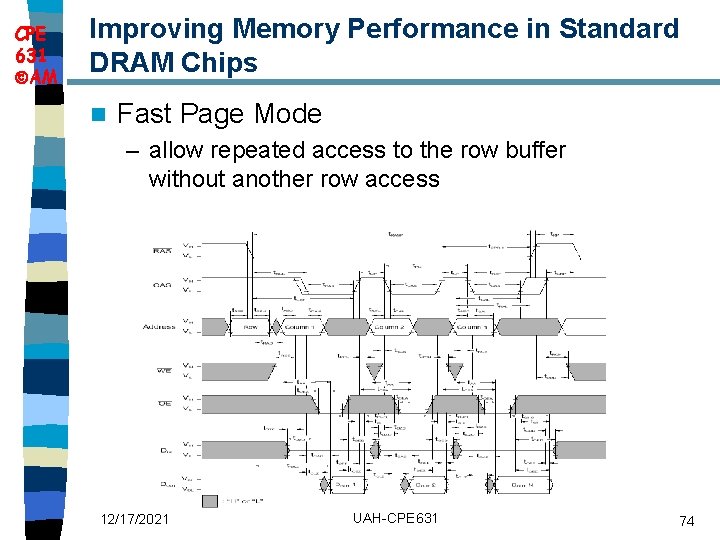
CPE 631 AM Improving Memory Performance in Standard DRAM Chips n Fast Page Mode – allow repeated access to the row buffer without another row access 12/17/2021 UAH-CPE 631 74

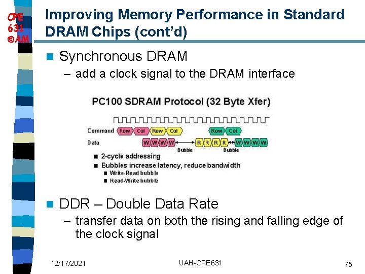
CPE 631 AM Improving Memory Performance in Standard DRAM Chips (cont’d) n Synchronous DRAM – add a clock signal to the DRAM interface n DDR – Double Data Rate – transfer data on both the rising and falling edge of the clock signal 12/17/2021 UAH-CPE 631 75

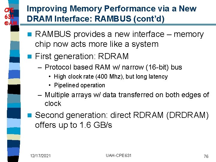
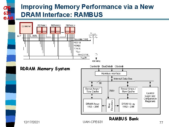
CPE 631 AM Improving Memory Performance via a New DRAM Interface: RAMBUS (cont’d) RAMBUS provides a new interface – memory chip now acts more like a system n First generation: RDRAM n – Protocol based RAM w/ narrow (16 -bit) bus • High clock rate (400 Mhz), but long latency • Pipelined operation – Multiple arrays w/ data transferred on both edges of clock n Second generation: direct RDRAM (DRDRAM) offers up to 1. 6 GB/s 12/17/2021 UAH-CPE 631 76

CPE 631 AM Improving Memory Performance via a New DRAM Interface: RAMBUS RDRAM Memory System 12/17/2021 UAH-CPE 631 RAMBUS Bank 77