COMPUTER SYSTEMS An Integrated Approach to Architecture and


- Slides: 43

COMPUTER SYSTEMS An Integrated Approach to Architecture and Operating Systems Chapter 3 Processor Implementation ©Copyright 2008 Umakishore Ramachandran and William D. Leahy Jr.

Processor Implementation • Implementation given an instruction set • Instruction-set is not a description of the implementation of the processor – Contract between hardware and software – Allows a compiler writer to generate code for different high-level languages to execute on a processor that implements this contract • Can there be different implementations of the same instruction set?

3. 1 Architecture versus Implementation • Market demands Why? • Parallel hardware and software development • Maintain compatibility for legacy software compatibility

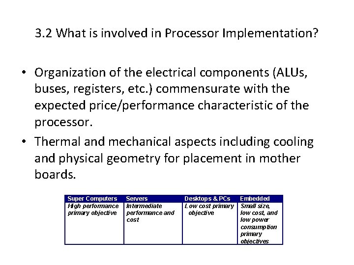
3. 2 What is involved in Processor Implementation? • Organization of the electrical components (ALUs, buses, registers, etc. ) commensurate with the expected price/performance characteristic of the processor. • Thermal and mechanical aspects including cooling and physical geometry for placement in mother boards. Super Computers High performance primary objective Servers Intermediate performance and cost Desktops & PCs Low cost primary objective Embedded Small size, low cost, and low power consumption primary objectives

3. 3 Key hardware concepts A review of important design principles

3. 3. 1 Circuits • Combinational logic – For a given set of inputs there is one unique output • Sequential logic – Circuits contain elements that remember state – Output demands on inputs and state

3. 3. 2 Hardware resources of the datapath • • • Memory ALU Register file Program Counter Instruction Register

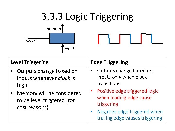
3. 3. 3 Logic Triggering outputs clock inputs Level Triggering • Outputs change based on inputs whenever clock is high • Memory will be considered to be level triggered (for cost reasons) Edge Triggering • Outputs change based on inputs only when clock transitions • Positive edge triggered logic when leading edge cause triggering • Negative edge triggered when trailing edge causes triggering

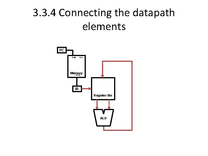
3. 3. 4 Connecting the datapath elements PC Addr Din Memory Dout IR Register-file ALU

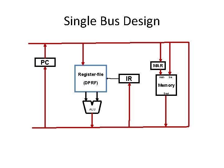
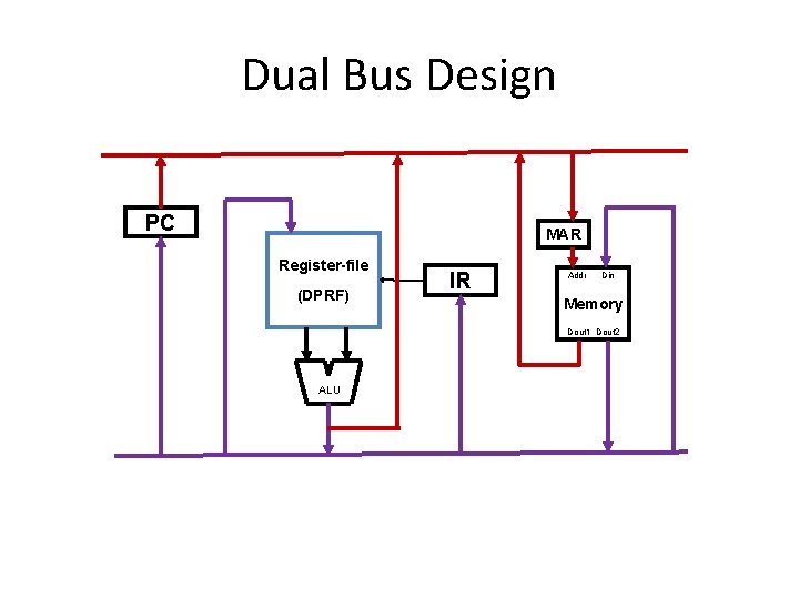
3. 3. 5 Towards bus-based Design • In principle we must make connections between circuit elements for every instruction • Numerous connections are expensive and take up valuable space • Have a set of wires that all elements can connect to and share in order to transfer information

Single Bus Design PC MAR Register-file (DPRF) IR Addr Din Memory Dout ALU

Dual Bus Design PC MAR Register-file (DPRF) IR Addr Din Memory Dout 1 Dout 2 ALU

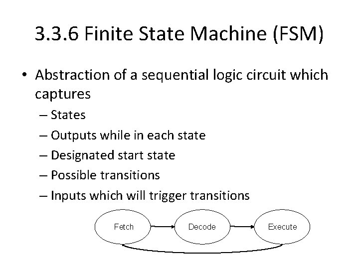
3. 3. 6 Finite State Machine (FSM) • Abstraction of a sequential logic circuit which captures – States – Outputs while in each state – Designated start state – Possible transitions – Inputs which will trigger transitions Fetch Decode Execute

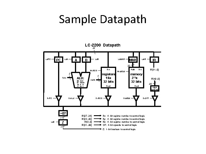
3. 4 Datapath Design • Processing Unit (CPU) consists of the Datapath and the Control Unit • Datapath is the combination of hardware resources and their connections • Example for LC-2200 – ALU capable of ADD, NAND, SUB, – Register file with 16 registers (32 -bit) shown in Figure 3. 14 – PC (32 -bit) – Memory with 232 X 32 bit words

Sample Datapath LC-2200 Datapath 32 PC Ld. PC A Ld. A B Ld. MAR IR Ld. IR MAR 32 Din Wr. REG 2 ALU: func 00: ADD 01: NAND 10: A - B 11: A + 1 Dr. PC 4 regno Dr. ALU =0? 1 Z Ld. Z 1 registers 16 x 32 bits Dout Dr. REG IR[27. . 24] IR[23. . 20] IR[3. . 0] IR[31. . 28] Wr. MEM Addr memory 232 x 32 bits IR[19. . 0] 20 Dout Dr. MEM Rx: Ry: Rz: OP: IR[31. . 0] Din sign extend Dr. OFF 4 -bit register number to control logic 4 -bit opcode to control logic Z: 1 -bit boolean to control logic

3. 4. 1 ISA and Datapath Width • We normally define a size for instructions, addresses and data operands (e. g. 32 bits) • Implementation could use bus and/or interconnects of smaller size (e. g. 8 or 16 bits) • Would require more operations to move a 32 bit value. Would require less chip real estate • Tradeoff speed vs. price

3. 4. 2 Width of the Clock Pulse • Combinational logic elements have a propagation delay. • Register files have an access time • Writing to a register requires input to be stable both before and after the leading edge of the clock arrives (set up time and hold time) • Wires have a transmission delay • Clock pulse must be wide enough to allow for all of the above

3. 4. 3 Checkpoint • You should now understand the following basic concepts – Basics of logic design including combinational and sequential logic circuits – Hardware resources for a datapath such as register file, ALU, and memory – Edge-triggered logic and how to arrive at the width of a clock cycle – Datapath interconnection and buses – Finite State Machines

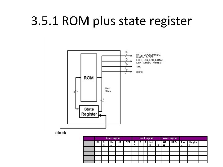
3. 5 Control Unit Design • The control unit is an implementation of the Finite State Machine • Depending on the current state and inputs it moves to the correct next state • Typical outputs from control unit (e. g. LC-2200) – – – Drive signals: Dr. PC, Dr. ALU, Dr. REG, Dr. MEM, Dr. OFF Load signals: Ld. PC, Ld. A, Ld. B, Ld. MAR, Ld. IR Write Memory signal: Wr. MEM Write Registers signal: Wr. REG ALU function selector: func Register selector: regno • Several alternatives exist for implementation

3. 5. 1 ROM plus state register Drive Signals PC . . . AL U Re g ME M Load Signals OFF P C A B MA R Write Signals I R ME M REG Fun c Reg. Se l

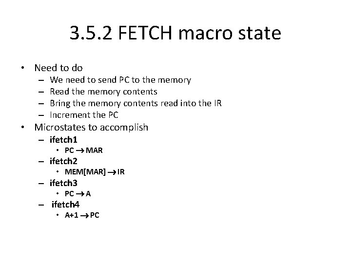
3. 5. 2 FETCH macro state • Need to do – – We need to send PC to the memory Read the memory contents Bring the memory contents read into the IR Increment the PC • Microstates to accomplish – ifetch 1 • PC MAR – ifetch 2 • MEM[MAR] IR – ifetch 3 • PC A – ifetch 4 • A+1 PC

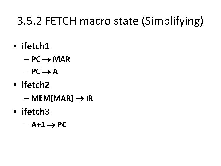
3. 5. 2 FETCH macro state (Simplifying) • ifetch 1 – PC MAR – PC A • ifetch 2 – MEM[MAR] IR • ifetch 3 – A+1 PC

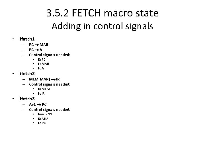
3. 5. 2 FETCH macro state Adding in control signals • ifetch 1 – PC MAR – PC A – Control signals needed: • Dr. PC • Ld. MAR • Ld. A • ifetch 2 – MEM[MAR] IR – Control signals needed: • Dr. MEM • Ld. IR • ifetch 3 – A+1 PC – Control signals needed: • func = 11 • Dr. ALU • Ld. PC

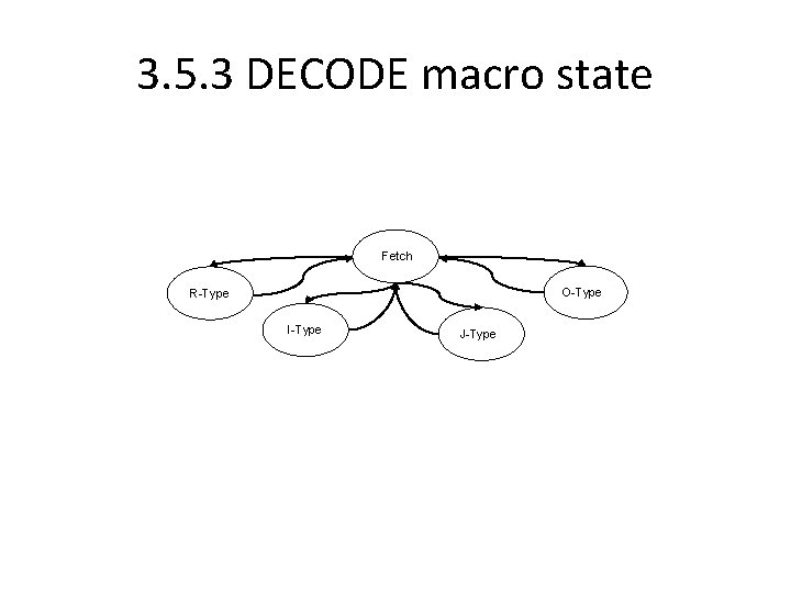
3. 5. 3 DECODE macro state Fetch O-Type R-Type I-Type J-Type

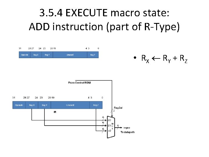
3. 5. 4 EXECUTE macro state: ADD instruction (part of R-Type) • RX RY + RZ

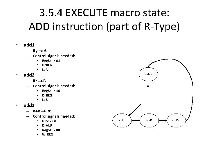
3. 5. 4 EXECUTE macro state: ADD instruction (part of R-Type) • add 1 – Ry A – Control signals needed: • add 2 • Reg. Sel = 01 • Dr. REG • Ld. A ifetch 1 – Rz B – Control signals needed: • add 3 . • Reg. Sel = 10 • Dr. REG • Ld. B – A+B Rx – Control signals needed: • • func = 00 Dr. ALU Reg. Sel = 00 Wr. REG . . add 1 add 2 add 3

3. 5. 5 EXECUTE macro state: NAND instruction (part of R-Type) • What must be changed in ADD to implement NAND?

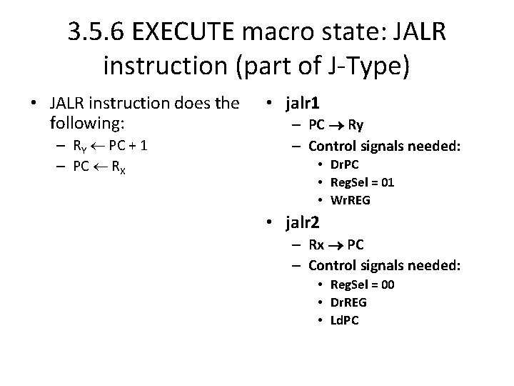
3. 5. 6 EXECUTE macro state: JALR instruction (part of J-Type) • JALR instruction does the following: – RY PC + 1 – PC RX • jalr 1 – PC Ry – Control signals needed: • Dr. PC • Reg. Sel = 01 • Wr. REG • jalr 2 – Rx PC – Control signals needed: • Reg. Sel = 00 • Dr. REG • Ld. PC

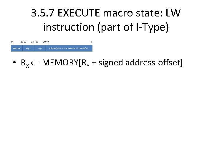
3. 5. 7 EXECUTE macro state: LW instruction (part of I-Type) • RX MEMORY[RY + signed address-offset]

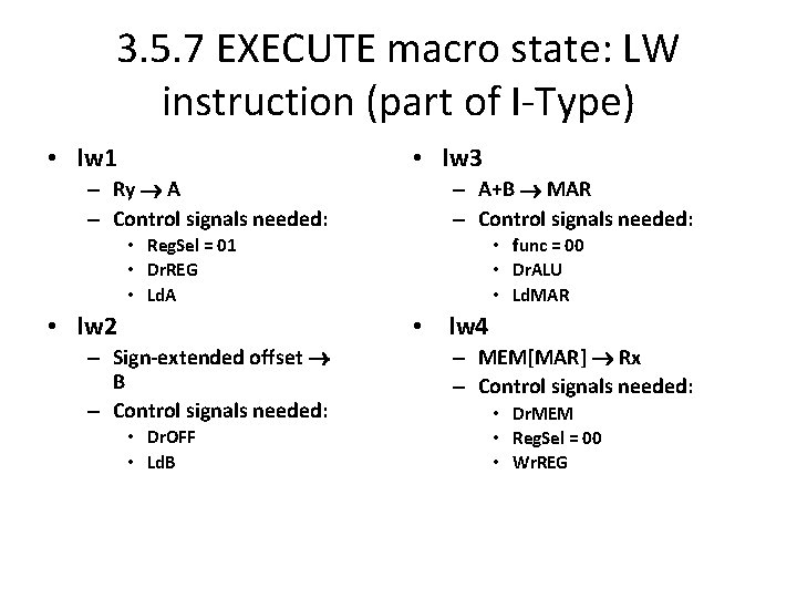
3. 5. 7 EXECUTE macro state: LW instruction (part of I-Type) • lw 1 • lw 3 – Ry A – Control signals needed: – A+B MAR – Control signals needed: • Reg. Sel = 01 • Dr. REG • Ld. A • lw 2 • lw 4 – Sign-extended offset B – Control signals needed: • Dr. OFF • Ld. B • func = 00 • Dr. ALU • Ld. MAR – MEM[MAR] Rx – Control signals needed: • Dr. MEM • Reg. Sel = 00 • Wr. REG

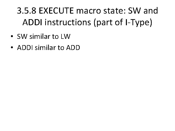
3. 5. 8 EXECUTE macro state: SW and ADDI instructions (part of I-Type) • SW similar to LW • ADDI similar to ADD

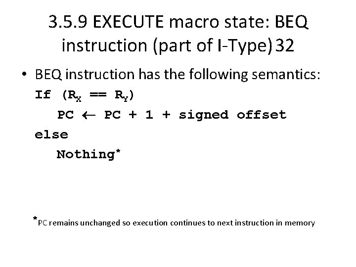
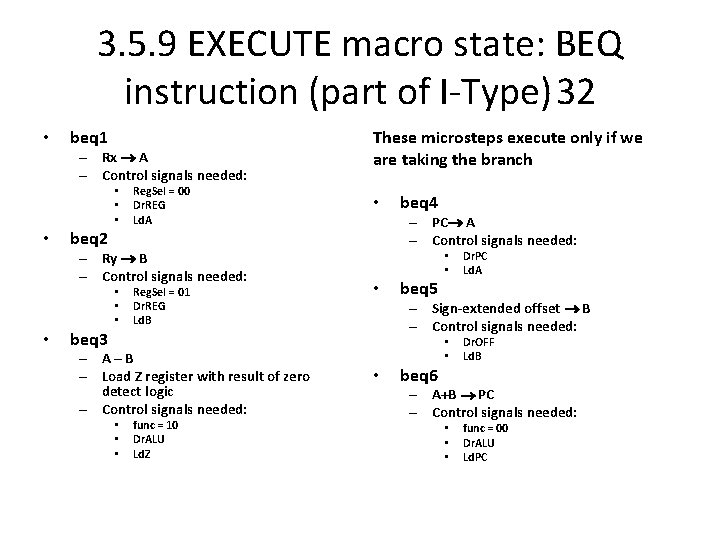
3. 5. 9 EXECUTE macro state: BEQ instruction (part of I-Type)32 • BEQ instruction has the following semantics: If (RX == RY) PC + 1 + signed offset else Nothing* *PC remains unchanged so execution continues to next instruction in memory

3. 5. 9 EXECUTE macro state: BEQ instruction (part of I-Type)32 • beq 1 – Rx A – Control signals needed: • • beq 2 Reg. Sel = 00 Dr. REG Ld. A – Ry B – Control signals needed: • • beq 3 Reg. Sel = 01 Dr. REG Ld. B – A – B – Load Z register with result of zero detect logic – Control signals needed: • • • func = 10 Dr. ALU Ld. Z These microsteps execute only if we are taking the branch • beq 4 – PC A – Control signals needed: • • • beq 5 Dr. PC Ld. A – Sign-extended offset B – Control signals needed: • • • beq 6 Dr. OFF Ld. B – A+B PC – Control signals needed: • • • func = 00 Dr. ALU Ld. PC

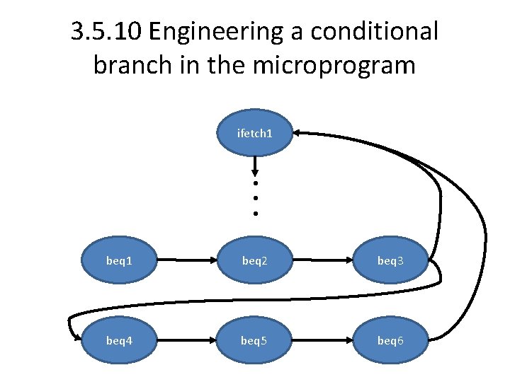
3. 5. 10 Engineering a conditional branch in the microprogram ifetch 1 • • • beq 1 beq 2 beq 3 beq 4 beq 5 beq 6

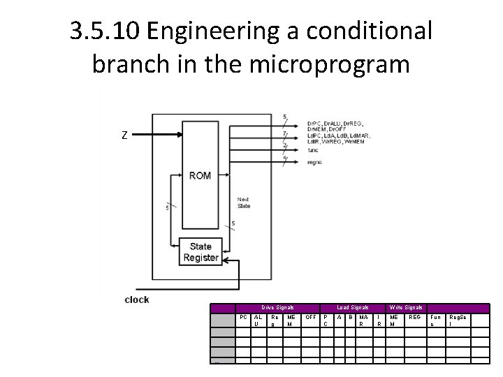
3. 5. 10 Engineering a conditional branch in the microprogram Z Drive Signals PC . . . AL U Re g ME M Load Signals OFF P C A B MA R Write Signals I R ME M REG Fun c Reg. Se l

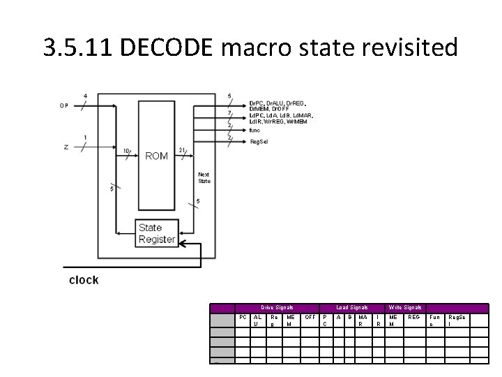
3. 5. 11 DECODE macro state revisited Drive Signals PC . . . AL U Re g ME M Load Signals OFF P C A B MA R Write Signals I R ME M REG Fun c Reg. Se l

3. 6 Alternative Style of Control Unit Design A number of different approaches may be used to implement the Control Unit

3. 6. 1 Microprogrammed Control • As presented our design works • Problem: Too slow – Solution: Prefetch the next microinstruction • Problem: Too much memory required – Solution: Have bit positions control different things as a function of opcode

3. 6. 2 Hardwired control • State machine can be represented as sequential logic truth table • Thus can be implemented using normal logic or FPGA

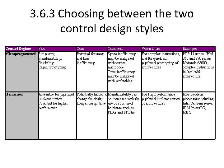
3. 6. 3 Choosing between the two control design styles Control Regime Pros Microprogrammed Simplicity, maintainability, flexibility Rapid prototyping Hardwired Cons Potential for space and time inefficiency Comment Space inefficiency may be mitigated with vertical microcode Time inefficiency may be mitigated with prefetching When to use For complex instructions, and for quick nonpipelined prototyping of architectures Examples PDP 11 series, IBM 360 and 370 series, Motorola 68000, complex instructions in Intel x 86 architecture Amenable for pipelined Potentially harder to Maintainability can For High performance implementation change the design be increased with the pipelined implementation Potential for higher Longer design time use of structured of architectures performance hardware such as PLAs and FPGAs Most modern processors including Intel Pentium series, IBM Power. PC, MIPS

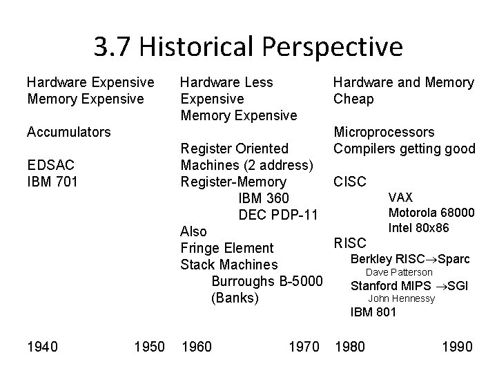
3. 7 Historical Perspective Hardware Expensive Memory Expensive Hardware Less Expensive Memory Expensive Accumulators Hardware and Memory Cheap Microprocessors Compilers getting good Register Oriented Machines (2 address) Register-Memory CISC VAX IBM 360 Motorola 68000 DEC PDP-11 Intel 80 x 86 Also RISC Fringe Element Berkley RISC Sparc Stack Machines Dave Patterson Burroughs B-5000 Stanford MIPS SGI John Hennessy (Banks) EDSAC IBM 701 IBM 801 1940 1950 1960 1970 1980 1990

Questions?
