ARM Ltd Designs the ARM range of RISC

: Applications processors for full")


 – Memory management support")


 • AMBA is a registered trademark")

 • The AMBA AHB is for high-performance, high")
 • The AMBA APB is for low-power peripherals.")


 includes the entire")

- Slides: 55
ARM Ltd • Designs the ARM range of RISC processor cores • Licenses ARM core designs to semiconductor • partners who fabricate and sell to their customers • ARM does not fabricate silicon itself. Also develop technologies to assist with the designin • of the ARM architecture • Software tools, boards, debug hardware • Application software Bus architectures • Peripherals, etc
• • • ARM Cortex-A family (v 7 -A): Applications processors for full OS and 3 rd party applications ARM Cortex-R family (v 7 -R): Embedded processors for real-time signal processing, control applications ARM Cortex-M family (v 7 -M): Microcontroller-oriented processors for MCU and So. C applications
• Processor Modes • User - used for executing most application programs • FIQ - used for handling fast interrupts • IRQ - used for general-purpose interrupt handling Supervisor - a protected mode for the Operating System • Undefined - entered upon Undefined Instruction exceptions • Abort - entered after Data or Pre-fetch Aborts • System - privileged user mode for the Operating System
• User - used for executing most application programs • � FIQ - used for handling fast interrupts • � IRQ - used for general-purpose interrupt handling • � Supervisor - a protected mode for the Operating System • � Undefined - entered upon Undefined Instruction exceptions • � Abort - entered after Data or Pre-fetch Aborts • � System - privileged user mode for the Operating System
• ARM cores implement two basic instruction sets – ARM instruction set – instructions are all 32 bits long – Thumb instruction set – instructions are a mix of 16 and 32 bits • Thumb-2 technology added many extra 32 - and 16 -bit instructions to the original 16 -bit Thumb instruction set • Depending on the core, may also implement other instruction sets – VFP instruction set – 32 bit (vector) floating point instructions – NEON instruction set – 32 bit SIMD instructions – Jazelle-DBX - provides acceleration for Java VMs (with additional software support) – Jazelle-RCT - provides support for interpreted languages
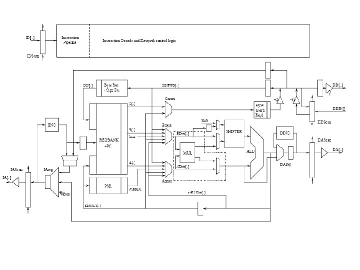
The ARM Register Set User mode r 0 r 1 r 2 r 3 r 4 r 5 r 6 r 7 r 8 r 9 r 10 r 11 r 12 r 13 (sp) r 14 (lr) r 15 (pc) IRQ FIQ Undef Abort SVC ARM has 37 registers, all 32 -bits long A subset of these registers is accessible in each mode Note: System mode uses the User mode register set. r 13 (sp) r 14 (lr) r 8 r 9 r 10 r 11 r 12 r 13 (sp) r 14 (lr) spsr spsr cpsr Current mode Banked out registers
Instruction Set basics • The ARM Architecture is a Load/Store architecture – No direct manipulation of memory contents – Memory must be loaded into the CPU to be modified, then written back out • Cores are either in ARM state or Thumb state – This determines which instruction set is being executed – An instruction must be executed to switch between states • The architecture allows programmers and compilation tools to reduce branching through the use of conditional execution – Method differs between ARM and Thumb, but the principle is that most (ARM) or all (Thumb) instructions can be executed conditionally.
Data Processing Instructions • These instructions operate on the contents of registers arithmetic logical move ADC SBC manipulation – They DO NOT affect memory ADD SUB RSB (has destination register) RSC BIC AND ORR EOR MVN MOV ORN comparison CMN CMP TST TEQ (set flags only) (ADDS) (SUBS) (ANDS) (EORS) • Syntax: <Operation>{<cond>}{S} {Rd, } Rn, Operand 2 • Examples: – ADD r 0, r 1, r 2 ; r 0 = r 1 + r 2
Suffix EQ NE CS/HS CC/LO MI PL VS VC HI LS GE LT GT LE AL Description Equal Not equal Unsigned higher or same Unsigned lower Minus Positive or Zero Overflow No overflow Unsigned higher Unsigned lower or same Greater or equal Less than Greater than Less than or equal Always Flags tested Z=1 Z=0 C=1 C=0 N=1 N=0 V=1 V=0 C=1 & Z=0 C=0 or Z=1 N=V N!=V Z=0 & N=V Z=1 or N=!V
Loading 32 bit constants • To allow larger constants to be loaded, the assembler offers a pseudo-instruction: • LDR rd, =const • This will either: – Produce a MOV or MVN instruction to generate the value (if possible). or – Generate a LDR instruction with a PC-relative address to read the constant from a literal pool (Constant data area embedded in the code). • For example – LDR r 0, =0 x. FF – LDR r 0, =0 x 5555 => => MOV r 0, #0 x. FF LDR r 0, [PC, #Imm 12] … … DCD 0 x 5555 • This is the recommended way of loading constants into a register
ARM Branches and Subroutines • B <label> – PC relative. ± 32 Mbyte range. • BL <subroutine> – Stores return address in LR – Returning implemented by restoring the PC from LR – For non-leaf functions, LR will have to be stacked func 1 func 2 : STMFD sp!, {regs, lr} : : : BL func 1 BL func 2 : : : LDMFD sp!, {regs, pc} : : MOV pc, lr
• Naming Rule of ARM {x} {y} {z} {T} {D} {M} {I} {E} {J} {F} {-S} –x: series –y: memory management / protection unit –z: cache –T: Thumb decoder –D: JTAG debugger –M: fast multiplier –I: support hardware debug –E: enhance instructions (based on TDMI) –J: Jazelle –F: vector floating point unit –S: synthesiable, suitable for EDA tools
SIMD
SIMD • Single Instruction, Multiple Data – – • • Single Instruction stream Multiple data streams Each instruction operate on multiple data in parallel Fine grained Level of Parallelism
SISD • Single Instruction Single Data – One stream of instruction – One stream of data • Scalar pipeline – To utilize CPU in most of the time • Super scalar pipeline – Increase throughput – Expecting to increase CPI > 1 • Improvement from increase the “operation frequency”
SISD
SIMD • • Example of SIMD operation SIMD code – Adding 2 sets of 4 32 -bits integers – V 1 = {1, 2, 3, 4} – V 2 = {5, 5, 5, 5} Vec. Load v 0, %0 (ptr vector 1) Vec. Load v 1, %1 (ptr vector 2) Vec. Add V 1, V 0 Or PMovdq mm 0, %0 (ptr vector 1) PMovdq mm 1, %1 (ptr vector 2) Paddwd mm 1, mm 0 Result V 2 = {6, 7, 8, 9}; Total instruction 2 load and 1 add Total of 3 instructions • SISD code – Adding 2 sets of 4 32 -bits integers – V 1 = {1, 2, 3, 4} – V 2 = {5, 5, 5, 5} Push ecx (load counter register) Mov %eax, %0 (ptr vector Mov %ebx, %1 (ptr vector . LOOP Add %%ebx, %%eax (v 2[i] = v 1[i] + v 2[i]) Add $4, %eax (v 1++) Add $4, %ebx (v 2++) Add $1, %eci (counter++) Branch counter < 4 Goto LOOP Result {6, 7, 8, 9) Total instruction 3 Load + 4 x (3 add) = 15 instructions
SIMD • A wide variety of applications can be solved by parallel algorithms with SIMD – only problems that can be divided into sub problems, all of those can be solved simultaneously by the same set of instructions – This algorithms are typical easy to implement
Superscalar • A superscalar CPU can execute more than one instruction per clock cycle. Because processing speeds are measured in clock cycles per second (megahertz), a superscalar processor will be faster than a scalar processor rated at the same megahertz. • A superscalar architecture includes parallel execution units, which can execute instructions simultaneously. This parallel architecture was first implemented in RISC processors, which use short and simple instructions to perform calculations. Because of their superscalar capabilities, RISC processors have typically performed better than CISC processors running at the same megahertz. However, most CISC-based processors (such as the Intel Pentium) now include some RISC architecture as well, which enables them to execute instructions in parallel. Nearly all processors developed after 1998 are superscalar.
• A superscalar CPU architecture implements a form of parallelism called instruction level parallelism within a single processor. It therefore allows faster CPU throughput than would otherwise be possible at a given clock rate. A superscalar processor executes more than one instruction during a clock cycle by simultaneously dispatching multiple instructions to redundant functional units on the processor. Each functional unit is not a separate CPU core but an execution resource within a single CPU such as an arithmetic logic unit, a bit shifter, or a multiplier. • While a superscalar CPU is typically also pipelined, pipelining and superscalar architecture are considered different performance enhancement techniques.
• Snytax of load and store instruction • LDR/STR {cond} <rd>, <addressing mode> • The addressing mode is indirect because the memory address is not to be specified directly in the instructio n • Indexed Addressing modes : • Pre indexed addressing mode • Effective address calculation is done before a load /store is executed. • Example : LDR R 0, [R 7, #4]
• Post indexed addressing mode • Effective address calculation is done after a load /store is executed. • Example : LDR R 0, [R 7], #4
• Read memory only and read write memory • The two memory area defined by the compiler are read only for code and Read/Write for data. • In the read only memory data is written using directives like DCD, DCW, etc. • From there it is copied to readwrite memory using laod and store instructions.
Area FIRST, CODE, READONLY ENTRY LDR R 7, = NUMS LDR R 8, =NUMS 1 LDR R 9, =NUMS 2 LDR R 1, [R 7] STR R 1, [R 9] STR R 1, [R 8] STOP B STOP NUMS DCD 653451134 AREA SECOND , DATA, READWRITE NUMS 2 SPACE 60 NUMS 1 DCD 0
Multiple Register Load / Store Instructions • Enable large quantities of data to be transferred more efficiently • They are used for procedure entry and exit to save and restore workspace registers • Copy blocks of data around memory LDM {COND} address-mode Rn{!}, reg-list{^} STM Store multiple registers LDMDA R 0, {R 4 -R 9} STMIA R 1, {R 2 -R 4} LDMIA r 1, {r 0, r 2, r 5} ; r 0 : = mem 32[r 1] ; r 2 : = mem 32[r 1 + 4] ; r 5 : = mem 32[r 1 + 8] The base register r 1 should be word-aligned
Addressing mode Description Starting address End address Rn! • • IA Increment After Rn Rn+4*N-4 Rn+4*N IB Increment Before Rn+4*N DA Decrement After Rn-4*Rn+4 Rn Rn-4*N DB Decrement Before Rn-4*N
• Application: Stack Operations • ARM use multiple load-store instructions to operate stack –POP: multiple load instructions –PUSH: multiple store instructions
Exception Handling • When an exception occurs, the ARM: – Copies CPSR into SPSR_<mode> – Sets appropriate CPSR bits • Change to ARM state • Change to exception mode • Disable interrupts (if appropriate) FIQ IRQ (Reserved) 0 x 1 C 0 x 18 0 x 14 0 x 10 – Stores the return address in LR_<mode> 0 x 0 C – Sets PC to vector address 0 x 08 Data Abort Prefetch Abort – Restore CPSR from SPSR_<mode> – Restore PC from LR_<mode> Reset Software Interrupt Undefined Instruction 0 x 04 • To return, exception handler needs to: 0 x 00 This can only be done in ARM state. Vector Table Vector table can be at 0 x. FFFF 0000 on ARM 720 T and on ARM 9/10 family devices
Application Processors
Embedded Processors
Development of the ARM Architecture v 4 Halfword and signed halfword / byte support System mode Thumb instruction set (v 4 T) v 5 Improved interworking CLZ Saturated arithmetic DSP MAC instructions Extensions: Jazelle (5 TEJ) v 6 SIMD Instructions Multi-processing v 6 Memory architecture Unaligned data support Extensions: Thumb-2 (6 T 2) Trust. Zone® (6 Z) Multicore (6 K) Thumb only (6 -M) v 7 Thumb-2 Architecture Profiles 7 -A - Applications 7 -R - Real-time 7 -M - Microcontroller § Note that implementations of the same architecture can be different § Cortex-A 8 - architecture v 7 -A, with a 13 -stage pipeline § Cortex-A 9 - architecture v 7 -A, with an 8 -stage pipeline
Which architecture processor?
Architecture ARMv 7 profiles • Application profile (ARMv 7 -A) – Memory management support (MMU) – Highest performance at low power • Influenced by multi-tasking OS system requirements – Trust. Zone and Jazelle-RCT for a safe, extensible system – e. g. Cortex-A 5, Cortex-A 9 • Real-time profile (ARMv 7 -R) – – Protected memory (MPU) Low latency and predictability ‘real-time’ needs Evolutionary path for traditional embedded business e. g. Cortex-R 4 • Microcontroller profile (ARMv 7 -M, ARMv 7 E-M, ARMv 6 -M) – – Lowest gate count entry point Deterministic and predictable behavior a key priority Deeply embedded use e. g. Cortex-M 3
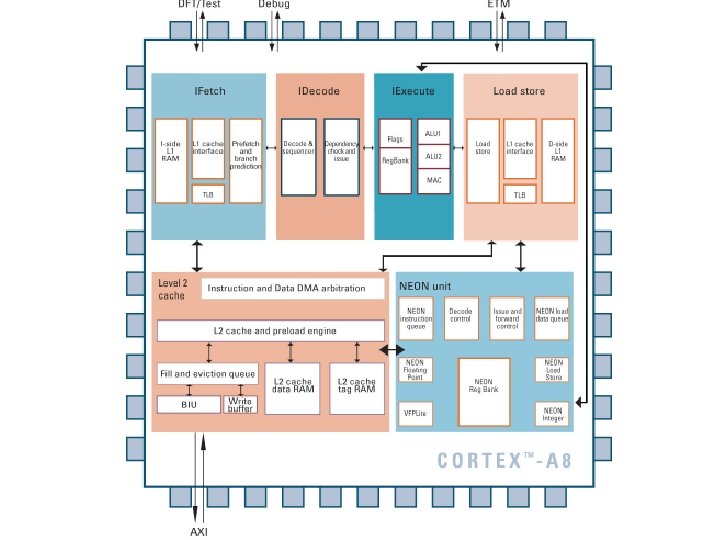
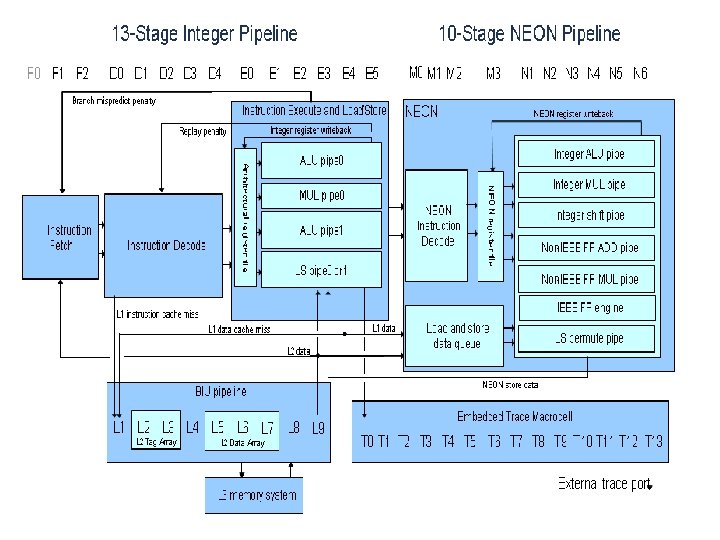
Cortex-A 8 • • • § Dual-issue, super-scalar 13 -stage pipeline § Branch Prediction & Return Stack § NEON and VFP implemented at end of pipeline ARMv 7 -A Architecture – Thumb-2 EE (Jazelle-RCT) – Trust. Zone extensions Custom or synthesized design MMU 64 -bit or 128 -bit AXI Interface L 1 caches – 16 or 32 KB each Unified L 2 cache – 0 -2 MB in size – 8 -way set-associative § Optional features § VFPv 3 Vector Floating-Point § NEON media processing engine
Exception handling process 1. Save processor status Main Application Sa Ch ve an pr ge oce st ss at or us s ta tu s – Copies CPSR into SPSR_<mode> – Stores the return address in LR_<mode> – Adjusts LR based on exception type 2. Change processor status for exception Exception handler – – Mode field bits ARM or Thumb state Interrupt disable bits (if appropriate) Sets PC to vector address 3. Execute exception handler – <users code> n tio ep xc e om fr rn tu Re 4. Return to main application – Restore CPSR from SPSR_<mode> – Restore PC from LR_<mode> • 1 and 2 performed automatically by the core • 3 and 4 responsibility of software
L 1 and L 2 Caches L 2 Cache ARM Core BIU MMU/MPU I-Cache RAM On-chip SRAM Off-chip Memory D-Cache RAM L 1 L 2 L 3 • Typical memory system can have multiple levels of cache – Level 1 memory system typically consists of L 1 -caches, MMU/MPU and TCMs – Level 2 memory system (and beyond) depends on the system design • Memory attributes determine cache behavior at different levels – Controlled by the MMU/MPU – Inner Cacheable attributes define memory access behavior in the L 1 memory system – Outer Cacheable attributes define memory access behavior in the L 2 memory system (if external) and beyond (as signals on the bus) • Before caches can be used, software setup must be performed
ARM 9 processors • The ARM 9 processor family is built around the ARM 9 TDMI processor. • Incorporates the 16 -bit Thumb instruction set. The ARM 9 Thumb family includes the ARM 920 T and ARM 922 T cached processor macrocells: • Dual 16 k and 8 K caches for applications running Symbian OS, Palm OS, Linux and Windows CE.
• The ARM 9 E processor family enables single processor solutions for microcontroller, DSP and Java applications. • The ARM 9 E family of products are DSP-enhanced 32 bit RISC processors, for applications requiring a mix of DSP and microcontroller performance. • The family includes the ARM 926 EJ-S, ARM 946 E-S, ARM 966 E-S, and ARM 968 E-S processor macrocells. They include signal processing extensions to enhance 16 -bit fixed point performance using a single-cycle 32 x 16 multiply-accumulate (MAC) unit, and implement the 16 -bit Thumb instruction set. • The ARM 926 EJ-S processor also includes ARM Jazelle technology which enables the direct execution of Java bytecodes in hardware.
• The ARM 926 EJ-S processor supports the ARM debug architecture and includes logic to assist in both hardware and software debug. • The ARM 926 EJ-S processor has a Harvard cached architecture and provides a complete highperformance processor subsystem, including: • an ARM 9 EJ-S integer core • a Memory Management Unit (MMU) • separate instruction and data AMBA AHB bus interfaces • separate instruction and data TCM (Tightly. Coupled Memory Interface interfaces. • AXI (Advanced e. Xtensible Interface)
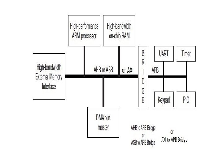
• The Advanced Microcontroller Bus Architecture (AMBA) • AMBA is a registered trademark of ARM Limited and is an open standard, on-chip interconnect specification for the connection and management of functional blocks in a System-on-Chip (So. C). • There are different bus protocols to satisfy different requirements such as speed, power, complexity depending on the type of devices or peripherals that need to be connected. • AMBA was introduced by ARM Ltd in 1996. The first AMBA buses were Advanced System Bus (ASB) and Advanced Peripheral Bus (APB).
• In its 2 nd version, AMBA 2, ARM added AMBA Highperformance Bus (AHB) that is a single clock-edge protocol. • In 2003, ARM introduced the 3 rd generation, AMBA 3, including AXI to reach even higher performance interconnect and the Advanced Trace Bus (ATB) as part of the Core. Sight on-chip debug and trace solution. • In 2010 the AMBA 4 specifications were introduced starting with AMBA 4 AXI 4, then in 2011[2] extending system wide coherency with AMBA 4 ACE. • In 2013[3] the AMBA 5 CHI (Coherent Hub Interface) specification was introduced, with a re-designed highspeed transport layer and features designed to reduce congestion.
• Advanced High-performance Bus (AHB) • The AMBA AHB is for high-performance, high clock frequency system modules. The AHB acts as the highperformance system backbone bus. AHB supports the efficient connection of processors, on-chip memories and off-chip external memory interfaces with lowpower peripheral macrocell functions. • Advanced System Bus (ASB) • The AMBA ASB is for high-performance system modules. AMBA ASB is an alternative system bus suitable for use where the high-performance features of AHB are not required. ASB also supports the efficient connection of processors, on-chip memories and off-chip external memory interfaces with lowpower peripheral macrocell functions.
• Advanced Peripheral Bus (APB) • The AMBA APB is for low-power peripherals. AMBA APB is optimized for minimal power consumption and reduced interface complexity to support peripheral functions. APB can be used in conjunction with either version of the system bus. • Advanced e. Xtensible Interface (AXI) • AXI, the third generation of AMBA interface defined in the AMBA 3 specification, is targeted at high performance, high clock frequency system designs and includes features that make it suitable for high speed sub-micrometer interconnect. AXI is faster and better performance than AHB. AMBA 4 completely gets rid of AHB and only defines AXI for high performance requirements.
• Clock cycle • The speed of a computer processor, or CPU, is determined by the clock cycle, which is the amount of time between two pulses of an oscillator. Generally speaking, the higher number of pulses per second, the faster the computer processor will be able to process information. The clock speed is measured in Hz, typically either megahertz (MHz) or gigahertz (GHz). For example, a 4 GHz processor performs 4, 000, 000 clock cycles per second. Computer processors can execute one or more instructions per clock cycle, depending on the type of processor. Early computer processors and slower processors can only execute one instruction per clock cycle, but faster, more advanced processors can execute multiple instructions per clock cycle, processing data more efficiently.
• Machine cycle The steps performed by the computer processor for each machine language instruction received. The machine cycle is a 4 process cycle that includes reading and interpreting the machine language, executing the code and then storing that code. Four steps of Machine cycle Fetch - Retrieve an instruction from the memory. Decode - Tranlate the retrieved instruction into a series of computer commands. Execute - Execute the computer commands. Store - Sand write the results back in memory.
• Instruction cycle • The sequence of operations that the cpu has to carry out while execution is called instruction cycle. • 1: - Read an Instruction • 2: - Decode the instruction • 3: - Find the address of operand • 4: - retrieve an operand • 5: - perform desired operation • 6: - find the address of destination • 7: - store the result into the destination
Cortex-A 8 • • • § Dual-issue, super-scalar 13 -stage pipeline § Branch Prediction & Return Stack § NEON and VFP implemented at end of pipeline ARMv 7 -A Architecture – Thumb-2 EE (Jazelle-RCT) – Trust. Zone extensions Custom or synthesized design MMU 64 -bit or 128 -bit AXI Interface L 1 caches – 16 or 32 KB each Unified L 2 cache – 0 -2 MB in size – 8 -way set-associative § Optional features § VFPv 3 Vector Floating-Point § NEON media processing engine
Basic pipeline description • Cortex A 8 is an in-order, dual-issue superscalar processor with in-order instruction issue, execution and retire. • The processor has a 13 -stage main pipeline that is used for all instructions. • The main pipeline can be broken into three parts: Fetch, Decode, and Execute. • The two Fetch stages at the front of the pipeline are responsible for predicting the instruction stream, fetching instructions from memory, and placing the fetched instructions into a buffer for consumption by the Decode pipeline.
• The five Decode stages take care of decoding, scheduling, and issuing instructions. They also deal with sequencing complex instructions and replaying instruction sequences when a memory stall occurs. • The six Execute stages consist of two symmetric ALU pipelines, a load-store pipeline, and a multiply pipeline. In addition to the mainpipeline, there is a 10 stage pipeline for the NEON SIMD execution engine,
Instruction Fetch Pipeline Overview • The Instruction Fetch unit (I-Fetch unit) includes the entire Level-1 Instruction side memory system as well as dynamic branch prediction, and instruction queuing hardware. • The Instruction Fetch pipeline runs decoupled from the rest of the processor, speculatively fetching up to four instructions per cycle along the predicted execution stream and placing them in the instruction queue to be consumed by the decode unit.
Trust. Zone Security • Trust. Zone adds a parallel world to run secure OS and applications • Normal and Secure worlds have different memory views, enforced by hardware • Memory tagged as secure and non-secure by the system – Only the secure CPU can access the secure memory & peripherals • Secure Monitor is a software “gatekeeper” between the two worlds • Device integrity, Digital Rights Management, Electronic payment, etc