ARM Advanced RISC Machines Scan and JTAG Principles
- Slides: 22

ARM Advanced RISC Machines Scan and JTAG Principles 1

Module Contents * Scan Fundamentals • Full and partial scan techniques • Level sensitive and edge triggered methods * JTAG and the Test Access Port (TAP) • JTAG Interface Signals • Test Access Port Controller • Test Access Port Instructions Scan and JTAG Principles 2

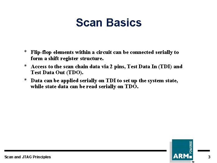
Scan Basics * Flip-flop elements within a circuit can be connected serially to form a shift register structure. * Access to the scan chain data via 2 pins, Test Data In (TDI) and Test Data Out (TDO). * Data can be applied serially on TDI to set up the system state, while state data can be read serially on TDO. Scan and JTAG Principles 3

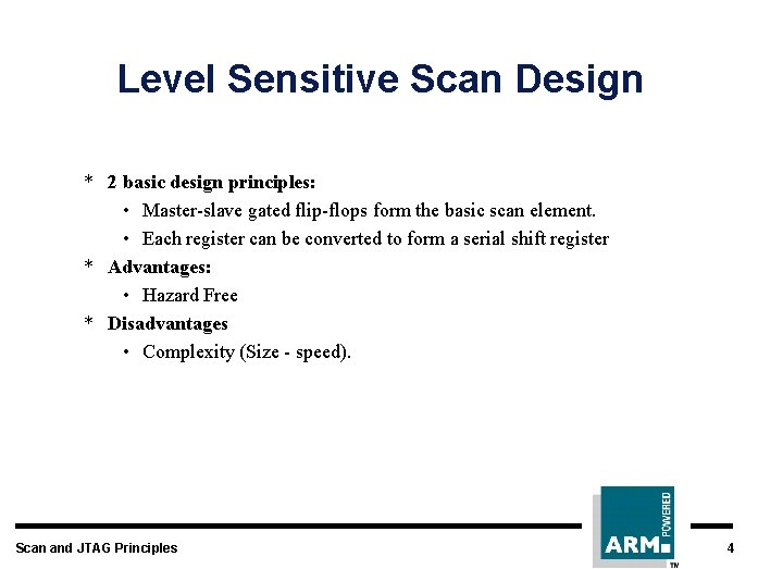
Level Sensitive Scan Design * 2 basic design principles: • Master-slave gated flip-flops form the basic scan element. • Each register can be converted to form a serial shift register * Advantages: • Hazard Free * Disadvantages • Complexity (Size - speed). Scan and JTAG Principles 4

Serial Scan * * Uses edge triggered latches to form the scan element. Lower complexity; higher speed. Sensitive to clock skew. May need synchronisation (redundant) opposite edge triggered scan elements to rectify. Scan and JTAG Principles 5

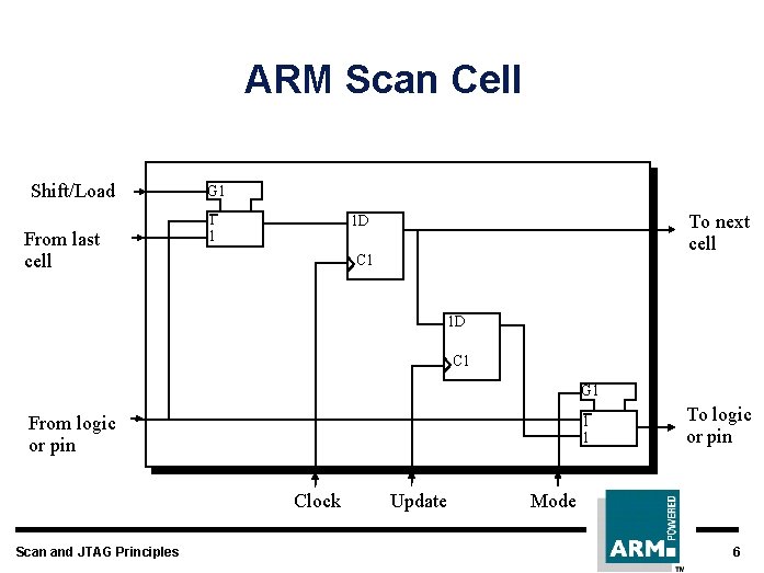
ARM Scan Cell Shift/Load From last cell G 1 1 1 To next cell 1 D C 1 G 1 1 1 From logic or pin Clock Scan and JTAG Principles Update To logic or pin Mode 6

Scan Nomenclature * Full Scan • Connection of all flip-flop elements into a single serial shift register. * Partial Scan • Connection of a subset of all flip-flop elements to form a serial shift register. • There can be more than one partial scan chain. * Boundary Scan • All I/Os are isolated from the core logic by a serial shift register. • This shift register can be used to apply system-level stimuli to the core serially. Scan and JTAG Principles 7

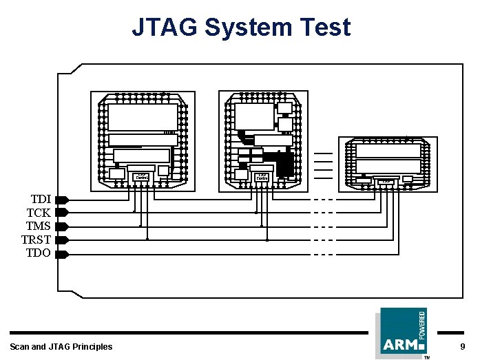
System Level Test * Increasing board complxities and use of multichip modules has stretched traditional system test techniques. * Joint Test Action Group (JTAG) to formulate a unified scan-based system test method. * Result was the IEEE 1149 Boundary Scan architecture. Scan and JTAG Principles 8

JTAG System Test TAP Control TAP TDI TCK TMS TRST TDO Scan and JTAG Principles 9

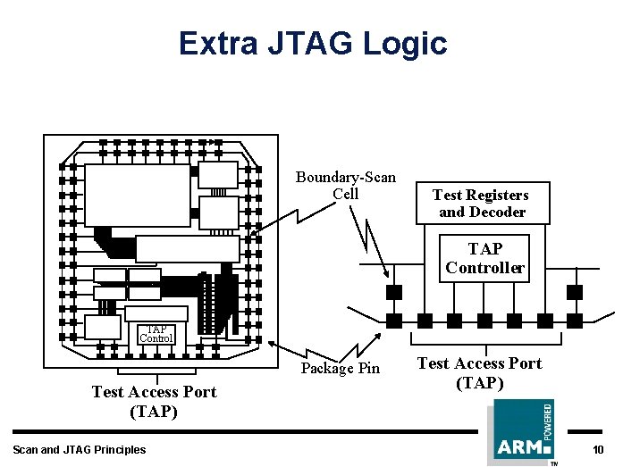
Extra JTAG Logic Boundary-Scan Cell Test Registers and Decoder TAP Controller TAP Control Package Pin Test Access Port (TAP) Scan and JTAG Principles Test Access Port (TAP) 10

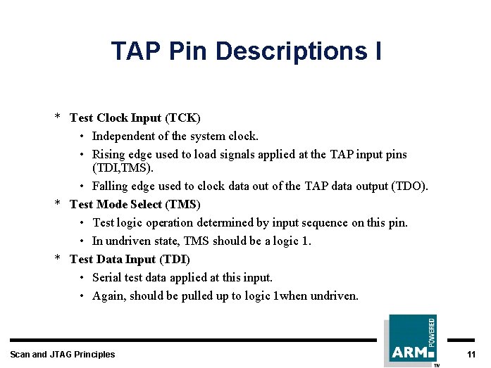
TAP Pin Descriptions I * Test Clock Input (TCK) • Independent of the system clock. • Rising edge used to load signals applied at the TAP input pins (TDI, TMS). • Falling edge used to clock data out of the TAP data output (TDO). * Test Mode Select (TMS) • Test logic operation determined by input sequence on this pin. • In undriven state, TMS should be a logic 1. * Test Data Input (TDI) • Serial test data applied at this input. • Again, should be pulled up to logic 1 when undriven. Scan and JTAG Principles 11

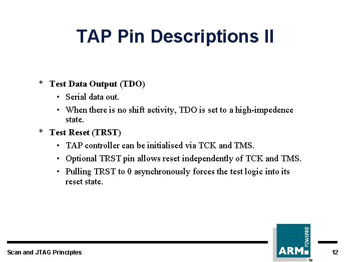
TAP Pin Descriptions II * Test Data Output (TDO) • Serial data out. • When there is no shift activity, TDO is set to a high-impedence state. * Test Reset (TRST) • TAP controller can be initialised via TCK and TMS. • Optional TRST pin allows reset independently of TCK and TMS. • Pulling TRST to 0 asynchronously forces the test logic into its reset state. Scan and JTAG Principles 12

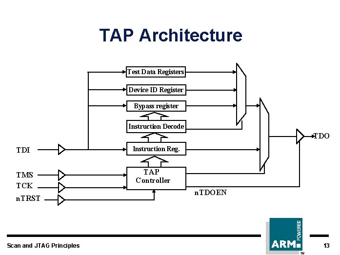
TAP Architecture Test Data Registers Device ID Register Bypass register Instruction Decode TDO TDI TMS TCK n. TRST Scan and JTAG Principles Instruction Reg. TAP Controller n. TDOEN 13

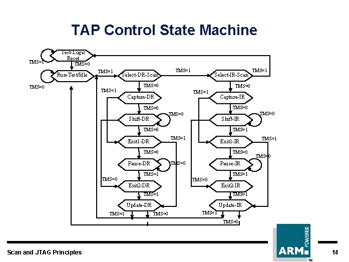
TAP Control State Machine TMS=1 Test-Logic Reset TMS=0 Run-Test/Idle TMS=0 TMS=1 Select-DR-Scan TMS=1 Select-IR-Scan TMS=0 TMS=1 Capture-DR TMS=0 Shift-IR TMS=0 Exit 1 -IR TMS=0 Pause-DR TMS=1 TMS=0 Pause-IR TMS=0 Exit 2 -DR TMS=1 Exit 2 -IR TMS=1 Update-DR TMS=1 TMS=0 TMS=1 Exit 1 -DR TMS=0 Capture-IR TMS=0 Shift-DR TMS=1 Update-IR TMS=0 TMS=1 TMS=0 Scan and JTAG Principles 14

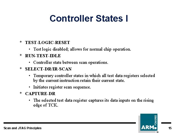
Controller States I * TEST-LOGIC-RESET • Test logic disabled; allows for normal chip operation. * RUN-TEST-IDLE • Controller state between scan operations. * SELECT-DR/IR-SCAN • Temporary controller states in which all test data registers selected by the current instruction retain their current state. • Initiates register scan sequence. * CAPTURE-DR • The selected test data register captures its data inputs on the rising edge of TCK. Scan and JTAG Principles 15

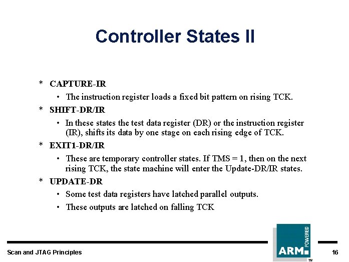
Controller States II * CAPTURE-IR • The instruction register loads a fixed bit pattern on rising TCK. * SHIFT-DR/IR • In these states the test data register (DR) or the instruction register (IR), shifts its data by one stage on each rising edge of TCK. * EXIT 1 -DR/IR • These are temporary controller states. If TMS = 1, then on the next rising TCK, the state machine will enter the Update-DR/IR states. * UPDATE-DR • Some test data registers have latched parallel outputs. • These outputs are latched on falling TCK Scan and JTAG Principles 16

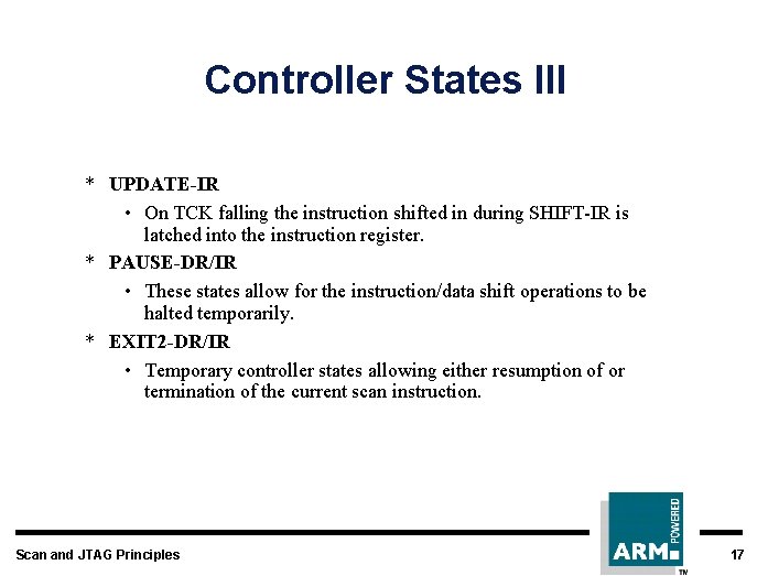
Controller States III * UPDATE-IR • On TCK falling the instruction shifted in during SHIFT-IR is latched into the instruction register. * PAUSE-DR/IR • These states allow for the instruction/data shift operations to be halted temporarily. * EXIT 2 -DR/IR • Temporary controller states allowing either resumption of or termination of the current scan instruction. Scan and JTAG Principles 17

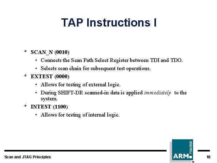
TAP Instructions I * SCAN_N (0010) • Connects the Scan Path Select Register between TDI and TDO. • Selects scan chain for subsequent test operations. * EXTEST (0000) • Allows for testing of external logic. • During SHIFT-DR scanned-in data is applied immediately to the system. * INTEST (1100) • Allows for testing of internal logic. Scan and JTAG Principles 18

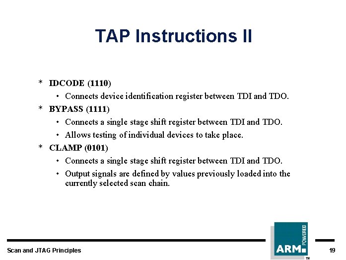
TAP Instructions II * IDCODE (1110) • Connects device identification register between TDI and TDO. * BYPASS (1111) • Connects a single stage shift register between TDI and TDO. • Allows testing of individual devices to take place. * CLAMP (0101) • Connects a single stage shift register between TDI and TDO. • Output signals are defined by values previously loaded into the currently selected scan chain. Scan and JTAG Principles 19

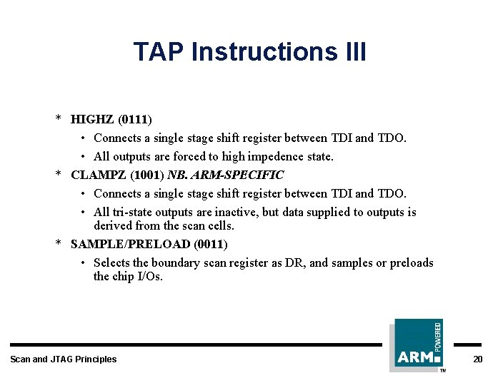
TAP Instructions III * HIGHZ (0111) • Connects a single stage shift register between TDI and TDO. • All outputs are forced to high impedence state. * CLAMPZ (1001) NB. ARM-SPECIFIC • Connects a single stage shift register between TDI and TDO. • All tri-state outputs are inactive, but data supplied to outputs is derived from the scan cells. * SAMPLE/PRELOAD (0011) • Selects the boundary scan register as DR, and samples or preloads the chip I/Os. Scan and JTAG Principles 20

ARM Implementation Details * * ARM 7 family cores have *no* boundary scan. SAMPLE/PRELOAD instructions must not be used. 3 Scan chains are available as test data registers. JTAG inputs (TDI and. TMS) have no internal pullups and must be driven correctly at all times. Scan and JTAG Principles 21

Summary * Serial test methods offer a route towards an automated method of providing test coverage. * IEEE 1149 extends this serial test architecture to cover system level testing. * ARM implements key components of the 1149 standard within its debug-aware cores, but requires external support to completely adhere to the standard. Scan and JTAG Principles 22