3 Advanced Rules Models Etienne Sicard etienne sicardinsatlse
- Slides: 27

3. Advanced Rules & Models Etienne Sicard etienne. sicard@insa-tlse. fr http: //intrage. insa-tlse. fr/~etienne 2/27/2021 1

Summary ØNew design rules ØMOS models (Model 1, 3, bsim 4) ØInterconnect model ØCrosstalk model ØConclusion 2/27/2021 2

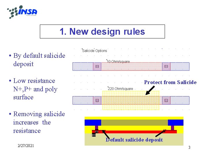
1. New design rules • By default salicide deposit • Low resistance N+, P+ and poly surface Protect from Salicide • Removing salicide increases the resistance Default salicide deposit 2/27/2021 3

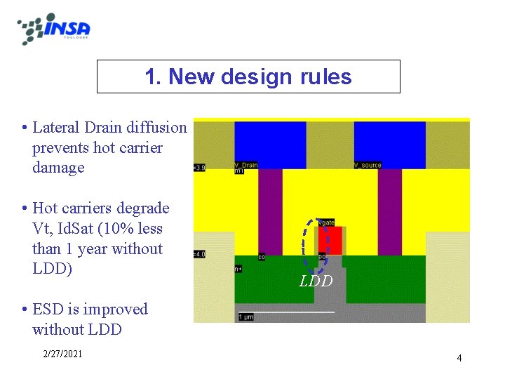
1. New design rules • Lateral Drain diffusion prevents hot carrier damage • Hot carriers degrade Vt, Id. Sat (10% less than 1 year without LDD) LDD • ESD is improved without LDD 2/27/2021 4

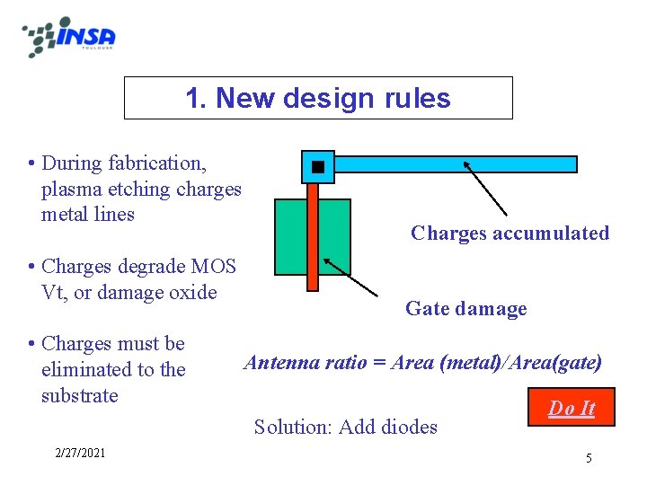
1. New design rules • During fabrication, plasma etching charges metal lines • Charges degrade MOS Vt, or damage oxide • Charges must be eliminated to the substrate Charges accumulated Gate damage Antenna ratio = Area (metal)/Area(gate) Solution: Add diodes 2/27/2021 Do It 5

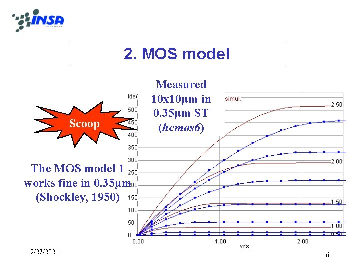
2. MOS model Scoop Measured 10 x 10µm in 0. 35µm ST (hcmos 6) The MOS model 1 works fine in 0. 35µm (Shockley, 1950) 2/27/2021 6

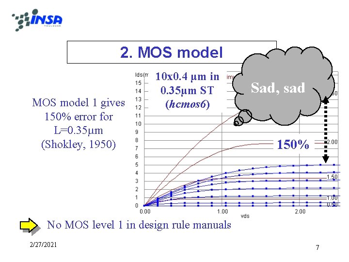
2. MOS model 1 gives 150% error for L=0. 35µm (Shokley, 1950) 10 x 0. 4 µm in 0. 35µm ST (hcmos 6) Sad, sad 150% No MOS level 1 in design rule manuals 2/27/2021 7

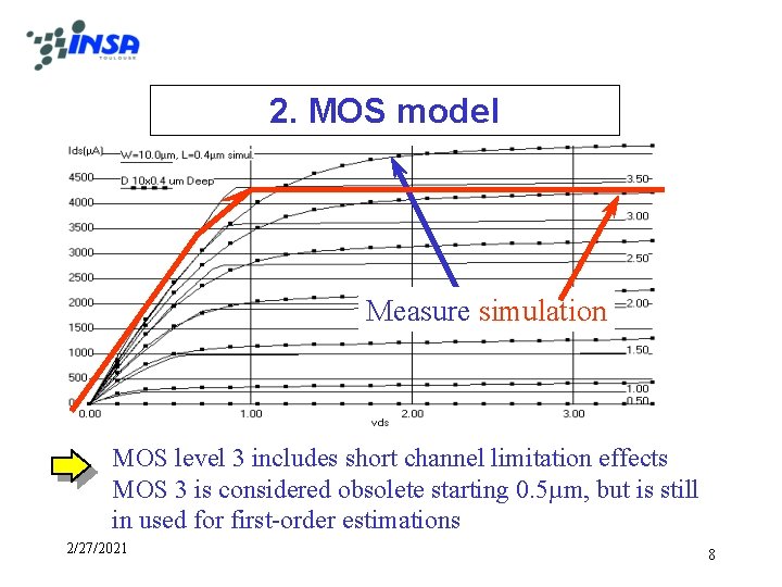
2. MOS model Measure simulation MOS level 3 includes short channel limitation effects MOS 3 is considered obsolete starting 0. 5µm, but is still in used for first-order estimations 2/27/2021 8

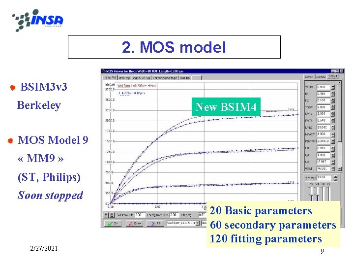
2. MOS model ® BSIM 3 v 3 Berkeley ® New BSIM 4 MOS Model 9 « MM 9 » (ST, Philips) Soon stopped 2/27/2021 20 Basic parameters 60 secondary parameters 120 fitting parameters 9

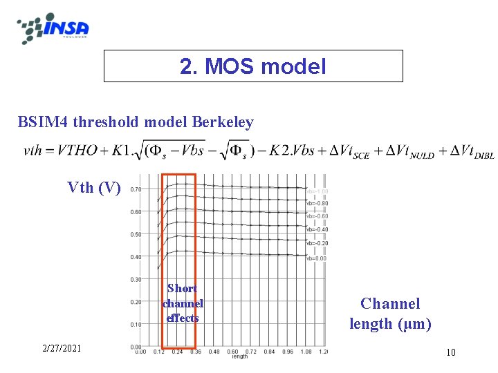
2. MOS model BSIM 4 threshold model Berkeley Vth (V) Short channel effects 2/27/2021 Channel length (µm) 10

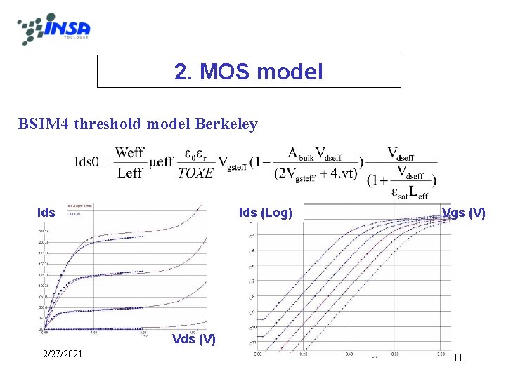
2. MOS model BSIM 4 threshold model Berkeley Ids (Log) Vgs (V) Vds (V) 2/27/2021 11

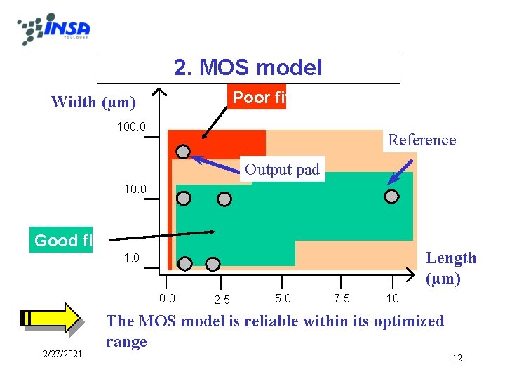
2. MOS model Poor fit Width (µm) 100. 0 Reference Output pad 10. 0 Good fit Length (µm) 1. 0 0. 0 2/27/2021 2. 5 5. 0 7. 5 10 The MOS model is reliable within its optimized range 12

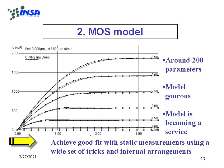
2. MOS model • Around 200 parameters • Model gourous 2/27/2021 • Model is becoming a service Achieve good fit with static measurements using a wide set of tricks and internal arrangements 13

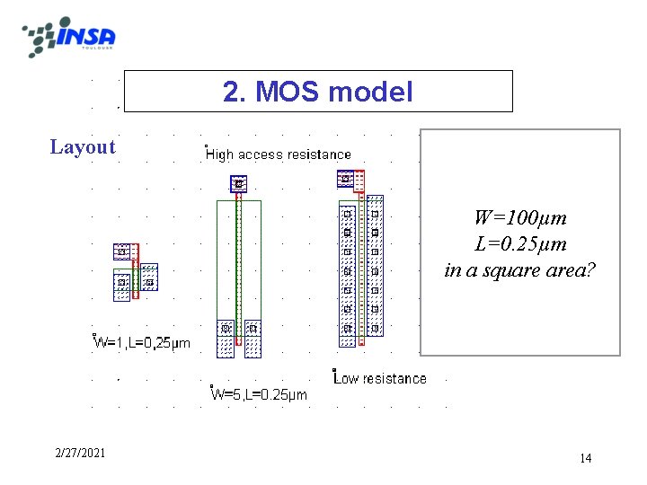
2. MOS model Layout W=100µm L=0. 25µm in a square area? 2/27/2021 14

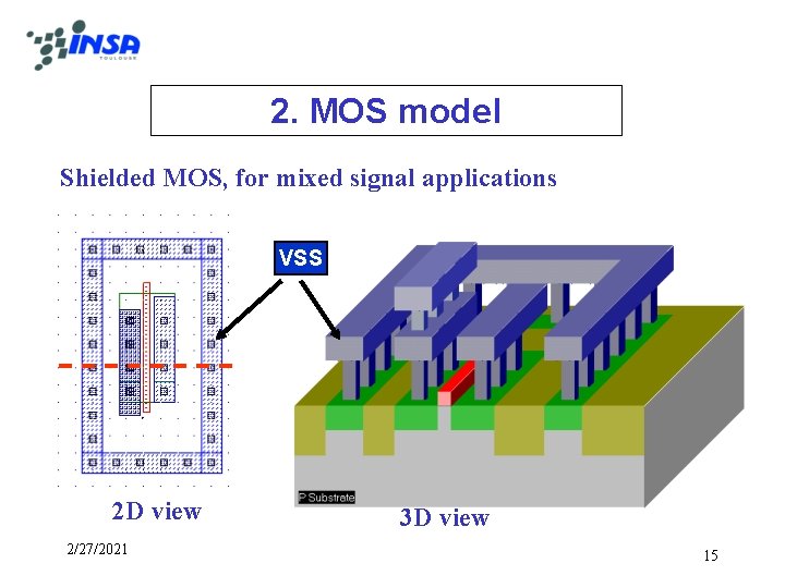
2. MOS model Shielded MOS, for mixed signal applications VSS 2 D view 2/27/2021 3 D view 15

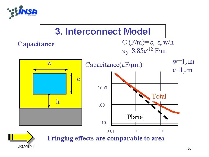
3. Interconnect Model C (F/m)= e 0 er w/h e 0=8. 85 e-12 F/m Capacitance w w=1µm e=1µm Capacitance(a. F/µm) e 1000 h Total 100 Plane 10 0. 01 0. 1 1. 0 Fringing effects are comparable to area 2/27/2021 16

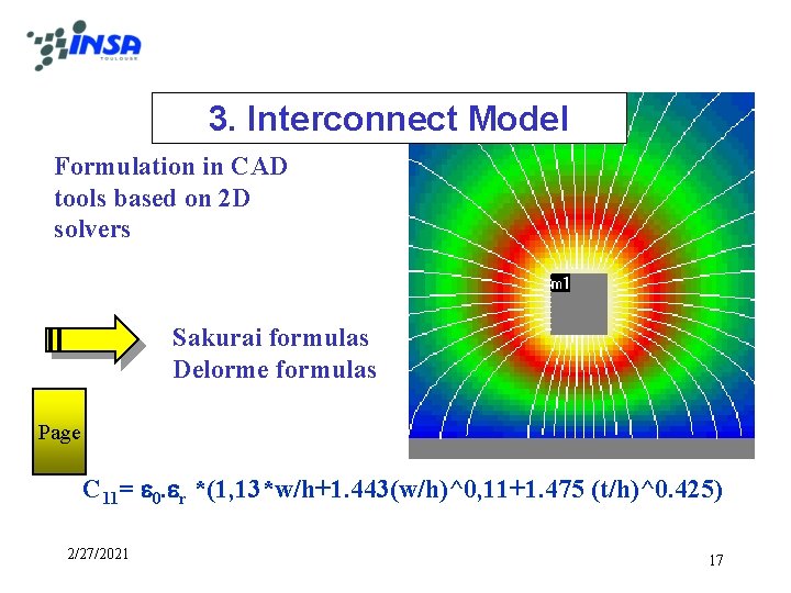
3. Interconnect Model Formulation in CAD tools based on 2 D solvers Sakurai formulas Delorme formulas Page C 11= 0. r *(1, 13*w/h+1. 443(w/h)^0, 11+1. 475 (t/h)^0. 425) 2/27/2021 17

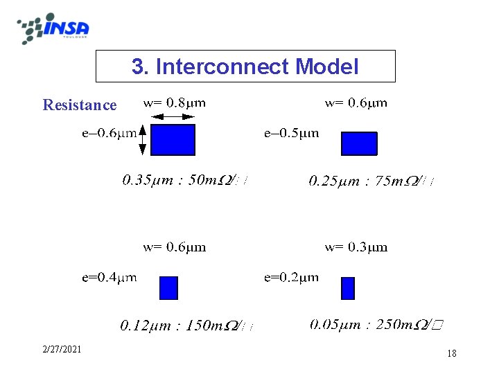
3. Interconnect Model Resistance 2/27/2021 18

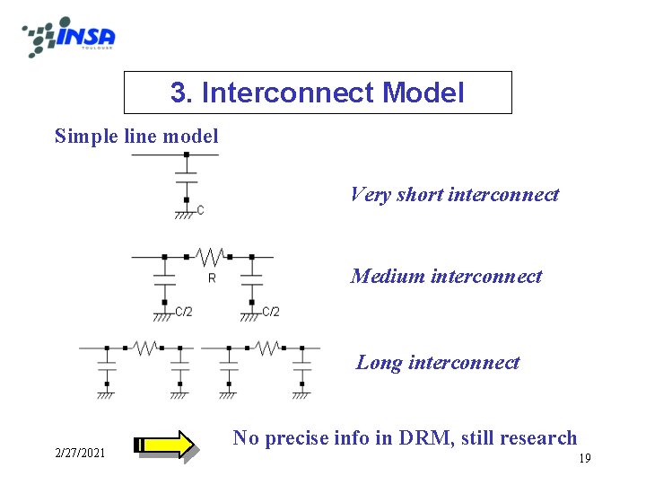
3. Interconnect Model Simple line model Very short interconnect Medium interconnect Long interconnect 2/27/2021 No precise info in DRM, still research 19

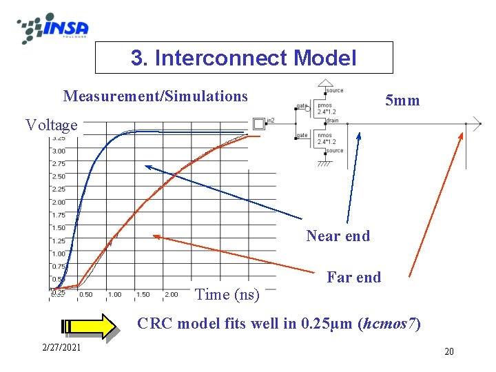
3. Interconnect Model Measurement/Simulations 5 mm Voltage Near end Time (ns) Far end CRC model fits well in 0. 25µm (hcmos 7) 2/27/2021 20

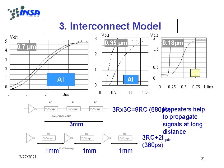
3. Interconnect Model Volt 5 Volt 3 0. 35 µm 0. 7 µm 4 Volt 2 1. 5 2 1 3 2 0. 5 1 Al 1 1 2 3 mm 1 mm 2/27/2021 0 0 3 ns 1 mm Cu 0 Al 0 0. 18µm 0. 5 1. 0 0. 25 0. 75 1. 0 ns 1. 5 ns Repeaters help 3 Rx 3 C=9 RC (680 ps) to propagate signals at long distance 3 RC+2 tgate (380 ps) 1 mm 21

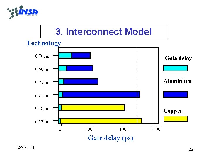
3. Interconnect Model Technology 0. 70µm Gate delay 0. 50µm Aluminium 0. 35µm 0. 25µm 0. 18µm Copper 0. 12µm 0 500 1000 1500 Gate delay (ps) 2/27/2021 22

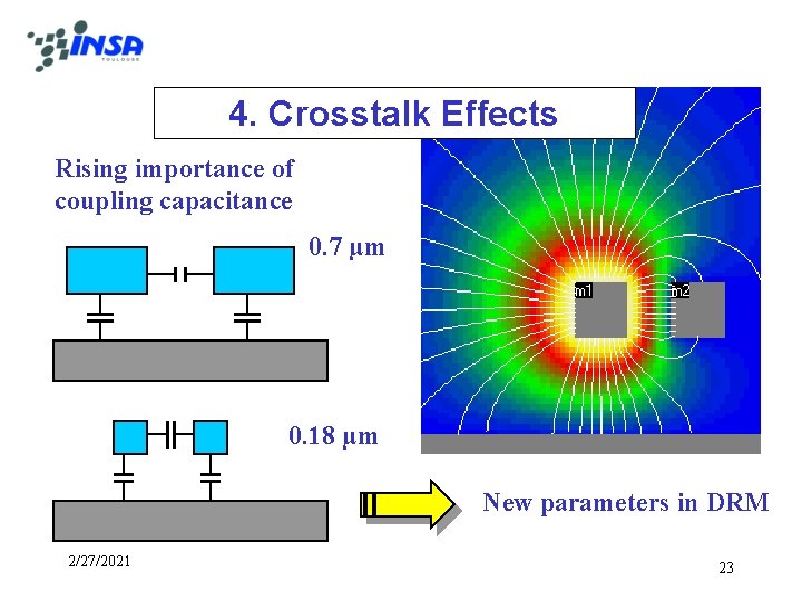
4. Crosstalk Effects Rising importance of coupling capacitance 0. 7 µm 0. 18 µm New parameters in DRM 2/27/2021 23

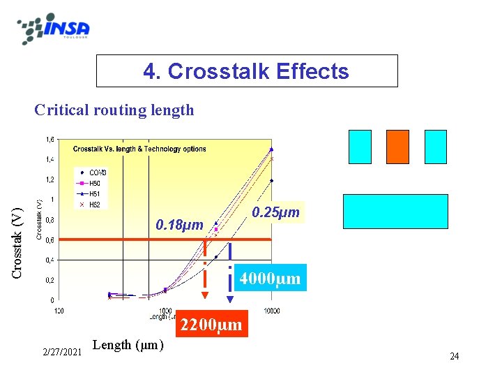
4. Crosstalk Effects Crosstak (V) Critical routing length 0. 25µm 0. 18µm 4000µm 2200µm 2/27/2021 Length (µm) 24

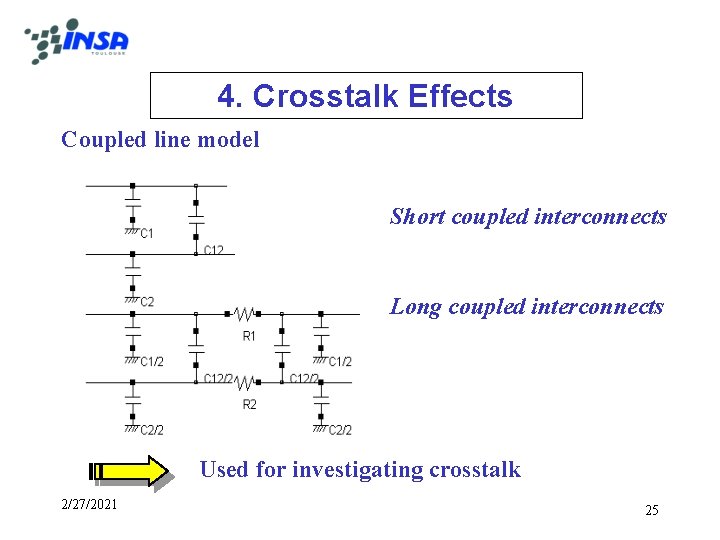
4. Crosstalk Effects Coupled line model Short coupled interconnects Long coupled interconnects Used for investigating crosstalk 2/27/2021 25

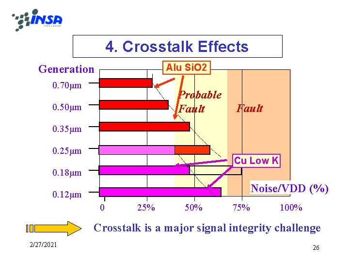
4. Crosstalk Effects Alu Si. O 2 Generation 0. 70µm Probable Fault 0. 50µm Fault 0. 35µm 0. 25µm Cu Low K 0. 18µm Noise/VDD (%) 0. 12µm 0 25% 50% 75% 100% Crosstalk is a major signal integrity challenge 2/27/2021 26

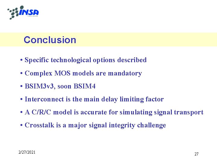
Conclusion • Specific technological options described • Complex MOS models are mandatory • BSIM 3 v 3, soon BSIM 4 • Interconnect is the main delay limiting factor • A C/R/C model is accurate for simulating signal transport • Crosstalk is a major signal integrity challenge 2/27/2021 27