1 VDSM and FullCustom Layout Design Issues2 kyungee
 경종민 kyung@ee. kaist. ac. kr")


 0. 3 1. 4 1. 2")


 and wire width(Wi) with fixed")

 and Wi(")
 Optimization")
 1. After initial TR/interconnect sizing 1647")


 Exact analysis 2) Early planning Switching PAD model Switching current model")


 IR-drop(V) 37. 8 42. 7 84 89. 9")
 at I/O driver • • • Output pad, Bi-direction")


 =2 1000 shielded, quiet")


 pair")


을")
 High density plasma")


 1. Antenna ratio Plasma source Gate poly-Si connected with")
 2. Plasma non-uniformity Plasma source Gate poly-Si connected with")
 3. ESE (Electron Shading Effect) ESE에 의한 F-N current")


 Cumulative Antenna ratio(CAR) = AR : Sinlge")
")


- Slides: 66
1 VDSM and Full-Custom Layout Design Issues(2) 경종민 kyung@ee. kaist. ac. kr
2 Contents • • Interconnect Modeling and Design IR drop and L*di/dt analysis Full Custom Datapath Design Antenna Rules
3 Interconnect Modelling and Design
4 Interconnect Scaling & Delay Capacitance (f. F/um) 0. 3 1. 4 1. 2 Ctotal 0. 25 Resis. 1. 0 0. 2 0. 8 0. 15 0. 6 0. 1 Ccoup 0. 05 0. 35 0. 4 Cover 0. 25 0. 18 0. 13 Feature size (um) 0. 2 0. 1 45 40 35 Delay in ps 0. 35 Resistance per length (ohms/um) Wire Delay vs. Gate Delay 30 Gate Delay Interconnect Delay, Al & Si. O 2 Interconnect Delay, Cu & Low K Sum of Delays, Al & Si. O 2 Sum of Delays, Cu & Low K 25 20 15 10 5 0 0. 65 0. 35 0. 25 0. 18 Generation(um) 0. 13 Interconnect contribution to signal delay Ccoup Cover 0. 1
5 Interconnect Modeling From above-1 um To below-0. 18 um Generation Technology > 1 um 1. 0 ~ 0. 5 um 0. 5~0. 25 um Resistance Ignored Lumped Distributed Area cap. Area, 2 D fringing 2/3 D fringing, Lat. coupling Capacitance Process Characterization Lat. coupling dominant Important Inductance Circuit model 0. 18 um > Lumped C Lumped RC Distributed RC RLC Transmission line Nominal modeling Statistical modeling
6 Extraction & Backannotation Flow calibrated technology file field solver Interconnect model library (process model ? ? ) layout file Parasitic Extractor - rule-based - library-based backannotation netlist enhanced netlist simulation & verification
7 Layout Design Methodology RTL Verilog re-optimize wire-model generation Synopsys slack >2 ns CTS, P/G, IO Saturn (buffer resizing) slack<2 ns Static timing (SDF/DSPF) Primetime Avant! Apollo(P&R) inter. guide wire Interconnect -planning statistics (wire model) floorplan Interconnect-Planning Synchronization 3 D extraction Clock skew star-RC power-ground noise I/O switching Time critical Bus Plan LVS/DRC Repeater Plan Hercules, Calibre
8 Interconnect Planning Process +Library plan. x Net-list Block Abstract P/G trunk, PAD (LEF, TDF, CMD) Floorplan (f. Plan) IR-drop IO SSN Coupling Clock Tree model EM model Noise model SPICE-level optimization High speed IO model P&R Guide P&R (Apollo) Static timing
9 Transistor/Interconnect Sizing PO PI considering both transistor width(wi) and wire width(Wi) with fixed wire width where i , gi 0 • Positive polynomial, posynomial
10 Optimization based on Posynomiality • Positive polynomial, posynomial – Solution space is convex, therefore, local optimum solution is globally optimal. • Geometric programming approach – Based on Newton’s method – Too slow for large circuits • Iterative approach – Local refinement until no more improvement – Tilos – Fast engineering solution
11 Table-Driven Iterative Sizing • Given initial sizing : wi (TR ) and Wi( Wire) • Optimize wi (or Wi) along the critical path – Determine wi (or Wi) with others fixed – Repeat until no more improvement • Delay evaluation – Analytic linear model : inexact – Simulation-based : very accurate but excessive CPU time – Table-driven • utilization of SPICE simulation data(delay/slope/power) • accurate and fast • Linear interpolation between data • Iteration between transistor sizing and interconnect sizing rather than solving for both simultaneously.
12 Ex. Repeater and Interconnect • 5200 m : RC limited Delay (ps) Optimization strategy 1100 After Initial TR/wire sizing 770 After Buffer optimizing 625 After Wire optimizing OPT(buf 1, buf 2, buf 3) = {70/27, 45/20, 78/30} OPT(wire 1, wire 2, wire 3) = {w=0. 94, s=1. 26}
13 Ex. Time-critical bus design 2525 ps(23 GD) 1. After initial TR/interconnect sizing 1647 ps(15 GD) 5. After segment buffer Trip point tuning Read. Bus<63: 0> Data. Bus<63: 0> LSData. Bus<63: 0> PLL I-cache Read. Bus<i+1> 2306 ps(21 GD) Write. Bus<i+1> 2. After evaluation Read. Bus<i> TR size optimizing Write. Bus<i> Read. Bus<i-1> Write. Bus<i-1> . . 1757 ps(16 GD) . 4. after segment Optimize (width, space, And interleaving . . . 1900 m within Load. Store datapath . . . Data. Bus<i+1> GND Code. Bus<i+1> Data. Bus<i> LSData. Bus<i>@phi 1 Code. Bus<i> Any. Bus<i>@phi 2 Data. Bus<i-1>. . Code. Bus<i-1>. . 1976 ps(18 GD) 3. After segment 2 Shieldinf and interleaving 1537 ps(14 GD) 6. After segment 3 Track assignment Branch History Load/ Store TLB . . . 4300 m global routing Fetch 2000 m within cache datapath D-cache TAG system Media Pipe Control MAC MEDIA/ MAC Control Unified Integer FPU RF 8000 mm 64 -bit bus • Careful interleaving of busses so that opposite transition between neighboring nets do not occur simultaneously • Functionally and Temporally exclusive bus • Power/GND : implicit shielding • Pre-charged busses (Read. Bus): monotonic transition Delay reduction from 23 GD to 14 GD, where 1 GD=110 ps n Clock frequency increased from 140 MHz to 200 MHz, Performance improve by 40%
14 IR drop and L* di/dt analysis
15 IR drop • Voltage drop in supply lines from current drawn by cells – Chip malfunctions on certain vectors – Performance degradation – Biggest problem : what’s the worst-case vector? Current depends on driver type, loads, and how often the cell is switched Voltage depends on currents of other cells Power supply network consists of wires of varying sizes; they must be big enough, but too big wastes area
16 Electro-migration • Power supply lines fail due to excessive current – More severe with DC path than AC path – Can be utilized as fuse • Prevention : wire cross-section to current rules – Maximum current density for particular materials (via layers) – Higher limits for short, thin wires due to grain effects – Copper : 100 x resistance to EM not a problem any more ? Current limit depends on wire size
17 Power IR-drop • IR-drop – Slows down the circuitry – Inhibits switching and incurs loss of state – Critical to maintain functionality and performance • IR drop is aggravated by – Smaller Transistor, longer interconnect – Long interconnect increasing resistance – High frequency which increases current density per die size • IR-drop is more serious than electromigration(? ) DV=I*R clean VDD V clean GND
18 Comparison between Previous Approaches and Proposed Approach • Previous approaches – Transistor level analysis at P&R stage – Long simulation time for exact current estimation in the full-chip power analysis – Huge RC netlist for power network – Large CPU time for iterations • Proposed approach – – RTL stage planning method based on floorplan Reducing turn-around-time Virtual power grid and current source Area-based DC current model
19 Optimization Flow Floorplan Power Virtual Netlist Generation Simulation IR-drop Analysis Star-sim Sizing of power network Sizing the width of power trunk, the number, and width of power refreshes within 10% IR-drop P&R Apollo
20 Comparison 1) Exact analysis 2) Early planning Switching PAD model Switching current model R(L)C network Transient analysis Constant drop PAD model Constant current model Resistance-only network DC analysis current 1) t 2) peak current average current
21 Standard cell Power Distribution • Assumption – Constant current source – Uniform grid resistance network P/G trunk P/G bus P/G refresh A A A
22 Full chip power distribution • Power trunk – Resistance network – Determine metal width • PAD – Determine location and its number • Block – Determine the number and the metal width of power refresh
23 Memory Power/Ground Best Case F Typical Case F Worst Case F
24 Final Result; Block current(m. A) IR-drop(V) 37. 8 42. 7 84 89. 9 95. 8 35. 9 77. 9 0. 154 0. 130 0. 089 0. 188 0. 139 0. 223 92. 3 99. 3 0. 105 0. 225 204. 3 0. 204 42. 7 0. 279 56. 9 0. 285 44. 2 39. 8 0. 269 0. 292 28. 4 0. 169 42. 9 66. 3 0. 279 0. 248 25. 6 0. 173 20. 8 0. 200 75. 7 83. 3 0. 302 0. 290 51. 2 56. 0 0. 261 0. 286 204. 3 0. 189 0. 206 68. 0 0. 265 45. 5 50. 5 0. 197 0. 218 68. 0 0. 265 70. 9 0. 087 17. 1 0. 061 75. 5 45. 5 52. 9 45. 5 0. 243 0. 182 0. 1250. 055 231. 9 0. 101 Block current(m. A) IR-drop(V) 120 m 60 m 30 m 20 m 80. 5 0. 100 22. 8 0. 138 26. 5 0. 219 Power metal width 30. 2 0. 119 Trunk width vs. IR-drop 60 m 0. 53 v 80 m 0. 45 v 100 m 0. 40 v 120 m 0. 35 v 140 m 0. 32 v
25 Simultaneous Switching Noise (SSN) at I/O driver • • • Output pad, Bi-direction pad 의 경우 큰 loading 에 따라 large transient current ( di/dt ) 가 흘러 ground bounce 발생. IO-limited design : Staggered I/O, 충분한 power 공급 문제 High Speed - Full swing issue : 외부 칩과의 동작에 대한 모델링 필요. VDDIO V 33 IO L R C output input Package model 388 PBGA + bonding wire and lead frame L = 20 n. H, R = 0. 4 ohm, C = 1. 5 p. F IO pad Package VSSIO PCB FR-4 PCB model(7 mil) L = 42 n. H, R = 10 ohm, C = 17 p. F
26 Power/Ground Bouncing VDDIO VDDcore VSS Power/Ground bouncing
27 High Speed I/O : speed, swing, power I/O Type Description Application Performan ce Features Benefits LVTTL /CMOS Pull/push I/O, LVTTL levels On board, chip-tochip 65 -100 MHz Push/Pull, LVTTL Standard I/O SSTL Used to improve operation in Situations where buses must be isolated from large stubs such as memory 200 MHz 4 class I, III, IV More drive flexibility, low voltage swing HSTL High-speed data communication such as DSP, fast computing systems, processor-to-memory To 250 MHz Low voltage swing, low power dissipation, good noise immunity, 4 classes offer more flexibility Low voltage swing & power dissipation, good noise immunity, 4 classes also variation in termination scheme (terminated/ unterminated/ series terminated) offer more design flexibility LVDS Low voltage differential signaling System-to-system communications for multiple parallel transaction and caches 1 Gb/s 250 -400 mv voltage swing, internal termination resistor High frequency, excellent noise immunity, low power consumption, low ratio of GND and Vcc pins relative to I/Os, no external resistor needed, handles multiple parallel transactions Giga. Blaze Full-duplex, gigabit serial interface Serial interface to high-speed protocols, parallel bus replacement in chipto-chip and board-toboard applications 3. 1 Gb/s Full-duplex capability doubles data rates, includes clock recovery circuit, meets Fibre Channel spec Excellent signal integrity by eliminating SSOs in board-toboard links Direct Rambus Channel interface High-speed chip-tomemory, graphics, multimedia, TV settop box converters 1. 6 Gbytes/s 800 MT/s, built-intestability, signal swing 0. 8 V High bandwidth with low pin count
28 Full Custom Datapath Design
29 Interconnect Capacitance 0. 25 m TLM 0. 60 m 0. 80 m 0. 4 m 0. 61 m 0. 80 m 0. 44 m 0. 69 m M 3 CV CH M 2 M 1 with length 1000 m(w=0. 44 m, s=0. 40 m) R=280 W Cwire(=CV+CH) Quiet neighbor CV: CH M 1 221 f. F(=101+120) 1: 1. 20 M 2 205 f. F(=90+115) 1: 1. 28 M 3 206 f. F(=54+152) 1: 2. 81 Opposite- M 1 341 f. F(=101+240) 1: 2. 38 switching M 2 319 f. F(=90+229) 1: 2. 54 neighbor M 3 358 f. F(=54+304) 1: 5. 63 u Pitch(=0. 84 m) and aspect ratio(=1. 36 ~ 2. 25) u Large horizontal capacitance causes higher coupling between wires.
30 Inter-wire Cross-coupling Effect L. Agg. Victim R. Agg. CV Ceff= · CH ( : switching activity factor) CH CH Left Aggressor CH Victim CH Right Aggressor bad situation =2 Right Aggressor good situation =0
31 Interconnect delay and Switching Behavior 1500 bad situation delay(ps) =2 1000 shielded, quiet neighbors =1 500 good situation =0 0. 4 u Wire 1. 2 2. 0 2. 8 3. 6 4. 4 5. 2 length(1000 m) RC delay on bus is strongly dependent on the switching behavior of neighbors.
32 Observation: • Reducing the Cross-Coupling ð Reducing the Effective Capacitance ð Reducing the Delay and Power due to Dynamic Switching • Policy: Reduce Ceff by reducing ij for wire pairs with large Cij. • In chip with datapath, there are many wire pairs with large Cij. The question is how to reduce ij by utilizing the properties of such wires.
33 Interconnect Layout in Datapath Control Signals <63> <i> <1> <0> Data Track
34 Ordering of Control Signal Wires distributed RC s 1 b s 2 s 3 s 4 s 2 b s 3 b s 4 b s 1 b s 2 b s 3 b s 4 b sel 1 sel 2 sel 3 coupling cap. u Most control signals are for multiplexer and usually lie on the time-critical path. u Control signals , si and sib make transition in the opposite direction and are vulnerable to be damaged by crosscoupling effect.
35 Datapath Cell Layout for mux …. . s 1 mux 3 …. . s 2 s 3 s 1 s 2 s 3 VDD s 1 b s 2 b s 3 b u Vertical : metal 3 data signal u Horizontal : metal 2 control signal VSS s 1 b s 2 b s 3 b
36 Control Signal Transition order 1 order 2 v Observation of opposite transitions s 1 s 1 b s 2 s 3 s 2 b s 1 b s 3 s 2 b s 3 b mux 3 t 11 t 12 s 2 t 22 t 32 u Try not to place si/sib pair in neighborhood t 31 t 23 u select (i) (siá, sibâ) deselect(i) (siâ, sibá) selection change (i àj) (siâ, sjá) and (sibá, sjbâ) v Suggestion s 1 t 13 t 21 u Try not to place si/sj pair in neighborhood s 3 t 33 Try not to place sib/sjb pair in neighborhood
37 New Control Signal Ordering Scheme Selection signal change Place only Si/Sjb(I j) pair in neighborhhood 1 ->2, 1 ->3 Equivalent cap. is reduced by 24 ~ 43 % u mux 3 : 1. 78 ( 1. 94 ) --> 1. 11 u mux 4 : 1. 50 ( 1. 67 ) --> 1. 14 order 2 proposed s 1 s 1 b s 2 b s 2 s 3 mux 3 s 2 b s 1 b s 3 s 2 b s 2 s 3 b All the opposite transitions are removed. u mux 3 : 12 ( 8 ) --> 0 u mux 4 : 24 ( 12) --> 0 order 1 order 2 proposed s 1 b s 2 b 0 s 3 b 1 s 2 0 s 3 s 1 b s 2 b s 3 b 1 s 2 b s 3 0 s 1 b s 2 s 3 b 1 2 ->1, 2 ->3 0 1 3 ->1, 3 ->2 Ceff 0 1 1 1 0 0 0 1 12 1. 78 0 1 0 # 1 0 1 1 0 0 1 8 1. 94 0 1. 11
38 Experimental Results 64 -bit datapath consisting of 3 -to-1 mux and 4 -to-1 mux, control signal length = 1000 m delay(ps) order 1 current(m. A) proposed Improve(%) order 1 proposed Improve(%) ex 0 486 433 10. 84 147. 489 136. 212 9. 94 ex 1 526 453 13. 78 155. 603 140. 141 7. 65 ex 2 502 421 16. 14 75. 037 66. 239 11. 72 ex 3 614 531 13. 52 93. 713 86. 332 7. 88 ex 4 652 579 11. 20 161. 42 153. 33 5. 00 ex 5 527 425 19. 39 72. 201 62. 8421 12. 96 ex 6 503 414 17. 69 73. 039 64. 128 12. 13 ex 7 546 474 13. 29 92. 013 83. 194 9. 58 ex 8 538 469 12. 79 93. 673 84. 713 9. 57 Avg 14. 3% 9. 6%
39 Density control for CMP • Cause of CMP variability – Pad deforms over metal frame – Greater ILD thickness over dense regions of layout – “Dishing” in sparse regions of layout • Layout density control – Modern foundry rules specify layout density bounds to minimize impact of CMP on yield – Uniform density achieved by post-processing, insertion of dummy features – Density rules control local feature density for Wx. W windows • eg. For metal layout every 2000 umx 2000 um window must be between 35% and 70% filled. • Filling = insertion of dummy feature to improve layout density – Accurate knowledge of filling is required during physical design and verification
40 Hot Electron Effect • Also called short-channel effect – Caused by extremely high E-field in the channel • Occurs when voltages are not scaled as fast as dimensions – Electron picks up speed in channel – Oxide and/or interface are damaged – Symptom : Threshold shift over time until chip fails • Prevention – Stay within the allowable region for input slew and output load – Set maximum allowed degradation over life of device – Size device as needed
41 Standard Cell
42 Standard cell Implementation Flow RTL description P&R synthesis Gate level netlist Final Layout
43 Custom Datapath • Datapath covers up to 60% of chip area especially for DSP applications. • Up to 40% chip area reduction compared to standard cell implementation. • More than 30% power saving is possible with optimized datapath implementation. • Compact datapath core as competitive IP.
44 Commercial Chip Datapath Bit-Slice Control Buffer Area
45 Custom Datapath Design Flow RTL description Schematic entry Micro-floorplan Final layout
46 Hand-crafted density based on the bitwise regularity
47 Mosaic Datapath compiler • Structure analysis and micro-floorplan – – – – • regularity analysis bus flow analysis element ordering track assignment routing analysis regular/irregular mixed placement pre-placement analysis Benefits – – – – reduced design-turn-around time: enable engineering change to be quickly analyzed reduced bit-wise skew improved routability predictable result design flexibility (bus row, aspect ratio) Hand-crafted density and performance Mixed Cell-based and bit-slice style layout Mixture of regular and irregular cell placement RTL HDL schematic Synthesis Netlist Microfloorplan P&R GDSII
48 Cell-based Datapath Compiler for Fast Error-free Design inv, tsbt nand 2, 3, 4 nor 2, 3 latl, lath regr pass mux 2 s, 3 s, 4 s mux 2 t, 3 t, 4 t : : • Various types of cell schematic library enables easy and fast schematic entry
49 Cell Generation with Automated Library Builder Symbolic Layout helps easy technology mapping Technology Migration takes advantage of existing layouts existing layout Symbolic layout Cell extraction compaction cell compaction target layout • technology file • cell geometry Mask layout Re-routing
50 Antenna Rule
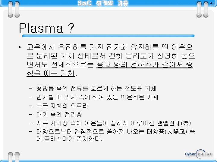
53 Plasma Damage • 반도체 제조 공정 중 Plasma를 이용한 공정 (etch or ash)을 통 하여 소자 (MOSFET)의 특성이 열화 되는 현상 – Physical damage (Silicon damage) • Energetic particle bombardment, polymer deposition, metal contamination – Junction leakage, contact resistance, minority carrier lifetime – Electrical damage (Gox damage) • Charging (Electrical trap), UV radiation – Gox leakage, device parameter shifts (Vth, Idsat), poor yield/reliability
54 왜 Plasma Damage가 최근의 Issue가 되었는가? 집적도의 증가 (CD의 감소) High density plasma Direct charging 증가 Multiple metal process Charging path 증가
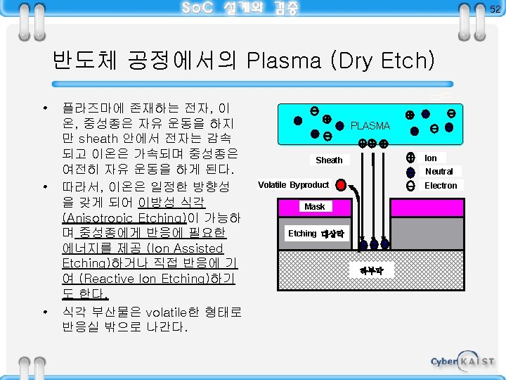
55 Cause of Plasma Damage Dry etching Plasma Antenna ratio non-uniformity Plasma ESE (Electron Shading Effect) Plasma damage
56 Antenna Rules • Charging in semiconductor processing – – – Many process steps use plasma, charges particles Charge collects on conducting poly, metal surfaces Capacitive coupling: large E fields over gate oxide Stresses cause damage, or complete breakdown Induce Vt shifts affect device matching (e. g, in analog) • Standard solution : Limit antenna ratio – Antenna ratio = (Apoly + Am 1 +. . ) / Agate-ox – Eg. Antenna ratio <300 – Amx metal(x) are electrically connected to node without using metal(x+1), and not connected to an active area • General solution == Bridging (break antenna by moving route to higher layer) • Antennas also solved by protection diodes – Not free (leakage power, area penalty)
57 Plasma Damage Mechanism (1/3) 1. Antenna ratio Plasma source Gate poly-Si connected with charge collecting antenna IP Source Field Ox. n+ Drain Gate n- n- n+ Field Ox. IFN p-Si substrate Grounded substrate Antenna ratio에 의한 F-N current 형성
58 Plasma Damage Mechanism (2/3) 2. Plasma non-uniformity Plasma source Gate poly-Si connected with charge collecting antenna IP 1 IP 2 Gate Field Ox. IFN 1 p-Si substrate IFN 2 IFN Floating substrate Plasma non-uniformity에 의한 F-N current 형성 Iplasma = Iions + Ielectrons
59 Plasma Damage Mechanism (3/3) 3. ESE (Electron Shading Effect) ESE에 의한 F-N current 형성 • High A/R 구조 Etching 시 Te >> Ti이므로 전자가 비 전도성 마스크 층에 포획됨 • Etching되는 도전체의 바 닥면은 양 이온으로 축적됨 • 축적된 양이온에 의해 Conducting Plug를 통한 Gate Oxide로의 FN Current를 형성하여 산화막 열화 촉진 • Layout Topology Dependent • Design Rule이 작아질수록 증가
60 Plasma Process에서의 Antenna Effect Plasma Met 2 Met 1 Source Field Ox. p-Si substrate n+ Drain Gate n- damage n- n+ Field Ox.
61 How To Calculate Antenna Ratio Single layer의 antenna ratio를 구한 후 process 진행 step과 동일하게 incremental accumulate한다. 1) Single layer Antenna ratio = Area of charge collecting layer on node Area of gate dielectric on node X 1 Antenna coeff. < Example > Antenna ratio 3 = 10 3+10+3+20 1 X 10 30 Antenna ratio 3 = 10 = 0. 12 3+10+3+20+8+10+8 1 X 10+12 30 = 0. 09 3 3 20 20 Antenna coeff. GPOLY 30 L 35 CNT/VIA 5 Metal 100 8 12 8
62 How To Calculate Antenna Ratio 2) Cumulative Antenna ratio(CAR) = AR : Sinlge layer antenna Ratio i : GPOLY ~ (TOP-1) metal < Example > Layer MOS 1 ∑ AR(i) MOS 2 MOS 1+MOS 2 10 2. 5 G-Poly (10*0. 35/1*0. 35) (5*0. 35/2*0. 35) N/A 0. 46 0. 23 Contact (0. 4*0. 4/1*0. 35) (0. 4*0. 4/2*0. 35) N/A Metal-1 N/A 76. 2 [(80*1)/(1*0. 35+2*0. 35)] Via-1 N/A 0. 15 [(0. 4*0. 4)/(1*0. 35+2*0. 35)] Metal-2 N/A Via-1(0. 4 x 0. 4) ● Metal-2 1/0. 35 10/0. 35 ● Cont(0. 4 x 0. 4) Poly MOS 1 MOS 3 5/0. 35 2/0. 35 N/A MOS 2 Poly ● Cont(0. 4 x 0. 4) Metal-1 (L/W=80/1) 1) CAR for MOS 1 : (10/30)+(0. 46/5)+(76. 2/100)+(0. 15/5)=1. 22 -> A diode connected to the gate electrode of a node provides a shunt path for the collected charge and, therefore, protects the node against antenna damage. Both N+/P-well and P+/N-well diodes are effective for this purpose. 2) CAR for MOS 2 : (2. 5/30)+(0. 23/5)+(76. 2/100)+(0. 15/5)=0. 92 -> This Transistor meets the rule CAR > 1 인 MOS 1이 Antenna error
63 How To Calculate Antenna Ratio - In case of 4 metal level (I) M 4 Via 3 M 3 Via 2 M 2 Via 1 MC G-poly N+ N+ - In case of 4 metal level (II) M 4 M 3 Via 2 M 2 Via 1 MC G-poly N+ N+ C. A. R. (Cumulative antenna ratio) 계산에 포함되어야 하는 layer
64 CAR 개선: Metal Routing Met 3 Met 2 Charged Plasma가 gate에 damage를 줌. Met 1 Gate Field Ox. p-Si substrate Met 3 Met 2 Met 1 Gate Field Ox. p-Si substrate Field Ox. Plasma가 discharge된 후에 gate와 연결 시킴.
65 CAR 개선: Plasma Damage Protection Diode vdd NWELL D 1 P+/N A=4 (2 u× 2 u) gate 2 um D 2 N+/P P-Sub A=4 (2 u× 2 u) 2 um vss Plasma에 의하여 charge되는 전하의 극성을 예측할 수 없기 때문에 양방향 diode를 gate와 연결 시킴. Metal Gate p+ Field Ox. n+ Nwell p-Si substrate
66 Antenna Rule Summary • Plasma Damage는 Dry Etching 공정에서 발생한다. • Plasma Damage의 발생 요인은 Antenna Ratio, Plasma Non-Uniformity, Electronic Shading Effect 등이 있다. • Antenna Ratio는 Plasma가 Charge되는 Conductor 의 면적과 Gate 면적 비를 Incremental Accumulate 하여 계산한다. • Antenna Fail은 Device 수율에 영향을 주므로, Metal Routing 또는 Protection Diode 등으로 대책을 마련 해야 한다.