FullCustom Design TYWu Outline n n n n








- Slides: 62
Full-Custom Design …. TYWu
Outline n n n n Introduction Transistor Process Steps Layout Schematic R/C Design Rules Tools
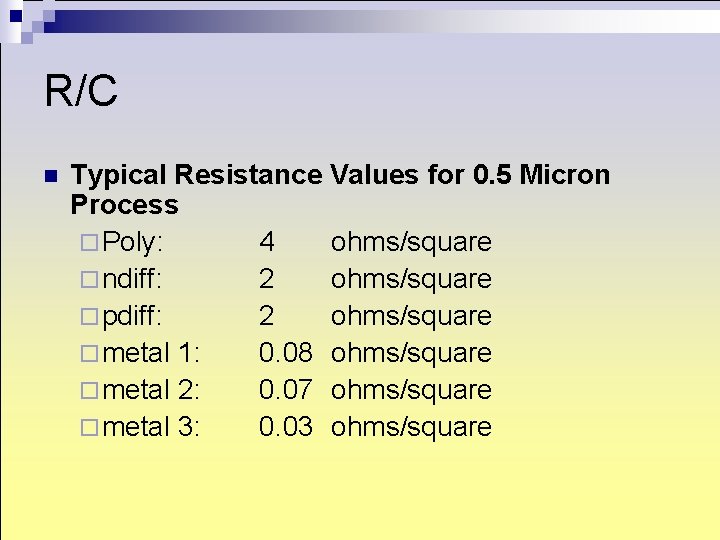
R/C n Typical Resistance Values for 0. 5 Micron Process ¨ Poly: 4 ohms/square ¨ ndiff: 2 ohms/square ¨ pdiff: 2 ohms/square ¨ metal 1: 0. 08 ohms/square ¨ metal 2: 0. 07 ohms/square ¨ metal 3: 0. 03 ohms/square
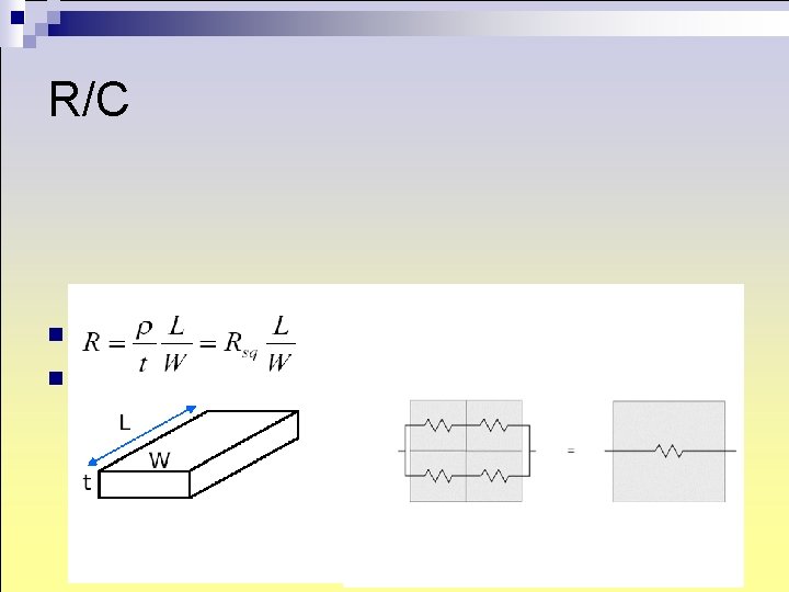
R/C n n How to Calculate Wire Resistance of any size square is constant
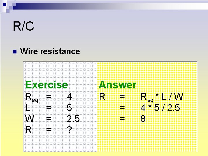
R/C n Wire resistance Exercise Answer Rsq L W R R = = 4 5 2. 5 ? = = = Rsq * L / W 4 * 5 / 2. 5 8
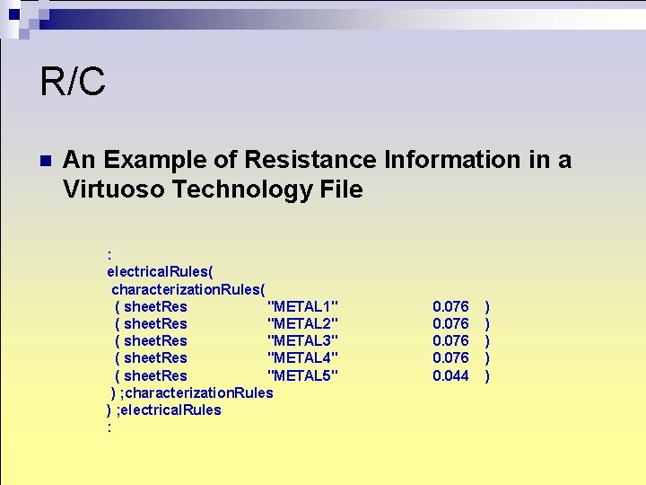
R/C n An Example of Resistance Information in a Virtuoso Technology File : electrical. Rules( characterization. Rules( ( sheet. Res "METAL 1" ( sheet. Res "METAL 2" ( sheet. Res "METAL 3" ( sheet. Res "METAL 4" ( sheet. Res "METAL 5" ) ; characterization. Rules ) ; electrical. Rules : 0. 076 0. 044 ) ) )
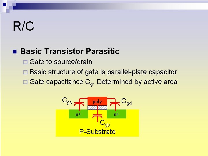
R/C n Basic Transistor Parasitic ¨ Gate to source/drain ¨ Basic structure of gate is parallel-plate capacitor ¨ Gate capacitance Cg. Determined by active area Cgs Cgd poly n+ n+ Cgb P-Substrate
R/C n Basic Transistor Parasitic ¨ Source/drain overlap capacitances Cgs, Cgd. Determined by source/gate and drain/gate overlaps. Independent of transistor L. Cgs = Col W Cgs Cgd poly n+ n+ Cgb P-Substrate
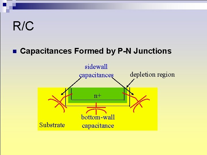
R/C n Capacitances Formed by P-N Junctions sidewall capacitances n+ Substrate bottom-wall capacitance depletion region
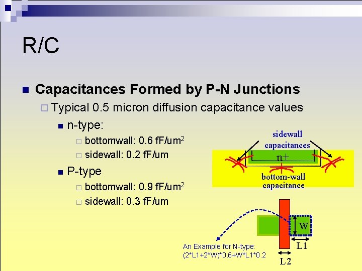
R/C n Capacitances Formed by P-N Junctions ¨ Typical 0. 5 micron diffusion capacitance values n n-type: bottomwall: 0. 6 f. F/um 2 ¨ sidewall: 0. 2 f. F/um ¨ n P-type bottomwall: 0. 9 f. F/um 2 ¨ sidewall: 0. 3 f. F/um ¨ sidewall capacitances n+ bottom-wall capacitance W An Example for N-type: (2*L 1+2*W)*0. 6+W*L 1*0. 2 L 1 L 2
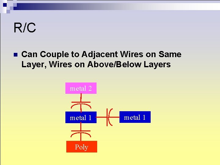
R/C n Can Couple to Adjacent Wires on Same Layer, Wires on Above/Below Layers metal 2 metal 1 Poly metal 1
R/C Metal 3 Metal 2 Metal 1 n Precise Parasitic Capacitance Includes 3 D Field Effect
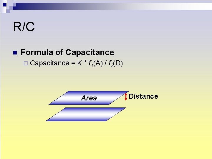
R/C n Formula of Capacitance ¨ Capacitance = K * f 1(A) / f 2(D) Area Distance
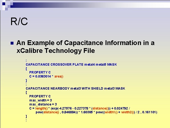
R/C n An Example of Capacitance Information in a x. Calibre Technology File : CAPACITANCE CROSSOVER PLATE metal 4 metal 5 MASK [ PROPERTY C C = 0. 0363014 * area() ] : CAPACITANCE NEARBODY metal 3 WITH SHIELD metal 3 MASK [ PROPERTY C max_width = 3 max_distance = 3 C = length() * (exp(-4. 27576 - 0. 227378 * (distance())) + 0. 024792 / pow(distance() , 0. 846884)) * 1. 60305 * pow((width 1() + width 2()) / 2 , 0. 161101) ] :
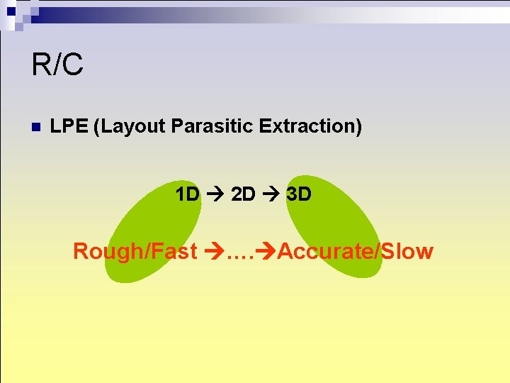
R/C n LPE (Layout Parasitic Extraction) 1 D 2 D 3 D Rough/Fast …. Accurate/Slow
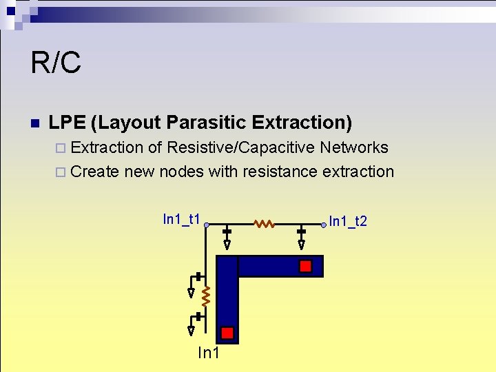
R/C n LPE (Layout Parasitic Extraction) ¨ Extraction of Resistive/Capacitive Networks ¨ Create new nodes with resistance extraction In 1_t 1 In 1_t 2
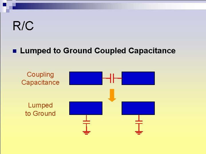
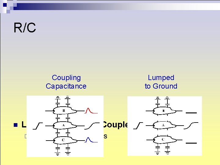
R/C n Lumped to Ground Coupled Capacitance Coupling Capacitance Lumped to Ground
R/C Coupling Capacitance n Lumped to Ground Coupled Capacitance ¨ Delay and Peak Noises
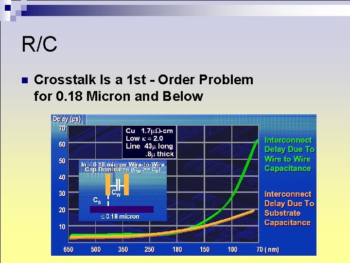
R/C n Crosstalk Is a 1 st - Order Problem for 0. 18 Micron and Below
R/C n R/C Reduction
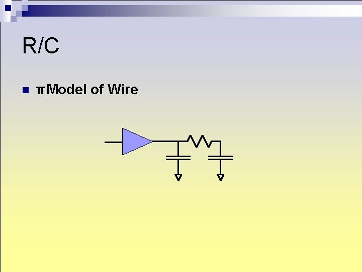
R/C n πModel of Wire
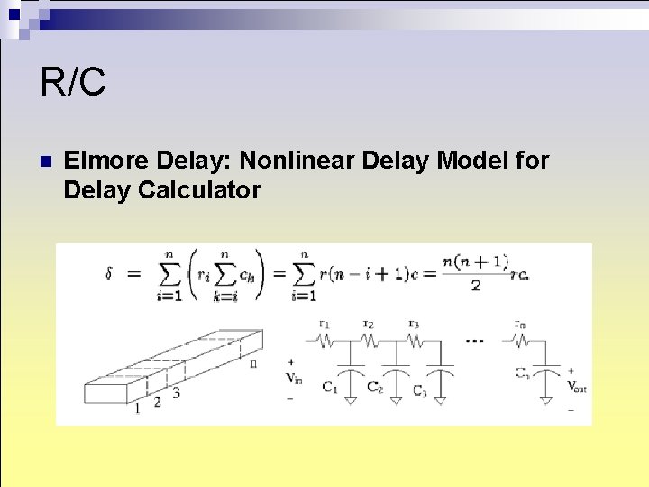
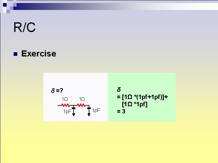
R/C n Elmore Delay: Nonlinear Delay Model for Delay Calculator
R/C n Exercise δ=? 1Ω 1 p. F δ = [1Ω *(1 pf+1 pf)]+ [1Ω *1 pf] =3
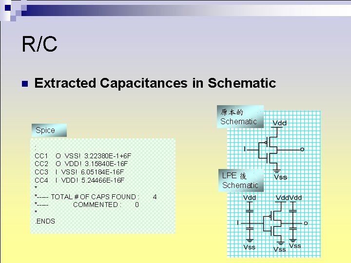
R/C n Extracted Capacitances in Schematic 原本的 Schematic Spice : CC 1 O VSS! 3. 22380 E-1+6 F CC 2 O VDD! 3. 15840 E-16 F CC 3 I VSS! 6. 05184 E-16 F CC 4 I VDD! 5. 24466 E-16 F * *----- TOTAL # OF CAPS FOUND : *----COMMENTED : 0 *. ENDS LPE 後 Schematic 4
R/C n Example for Pre/Post-layout Simulation Pre-sim Post-sim
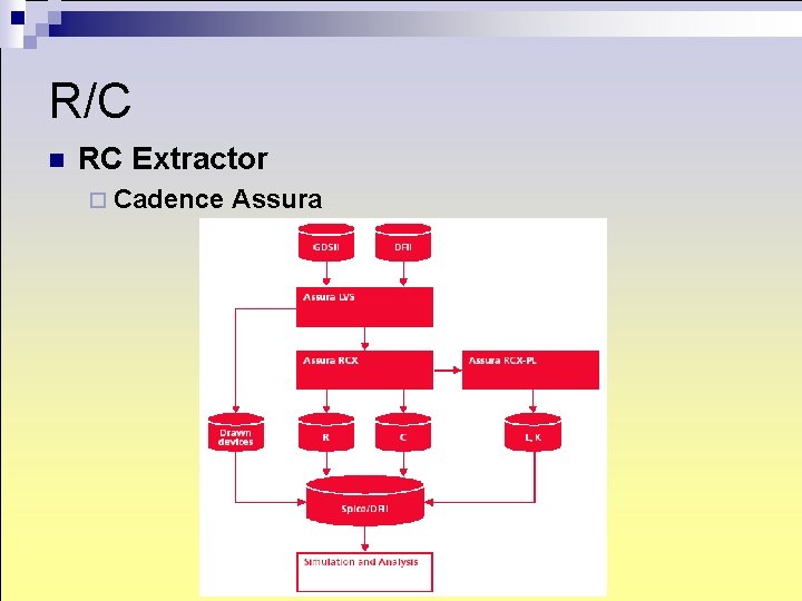
R/C n RC Extractor ¨ Cadence Assura
R/C n RC Extractor ¨ Synopsys Star-RCXT
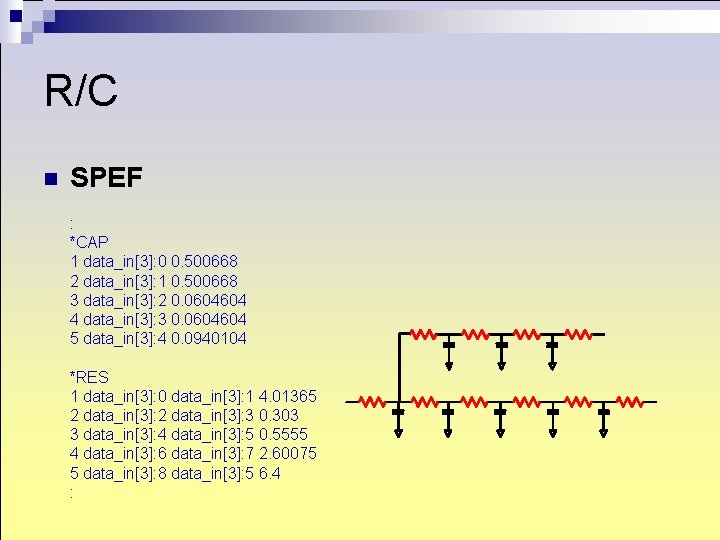
R/C n SPEF : *CAP 1 data_in[3]: 0 0. 500668 2 data_in[3]: 1 0. 500668 3 data_in[3]: 2 0. 0604604 4 data_in[3]: 3 0. 0604604 5 data_in[3]: 4 0. 0940104 *RES 1 data_in[3]: 0 data_in[3]: 1 4. 01365 2 data_in[3]: 3 0. 303 3 data_in[3]: 4 data_in[3]: 5 0. 5555 4 data_in[3]: 6 data_in[3]: 7 2. 60075 5 data_in[3]: 8 data_in[3]: 5 6. 4 :
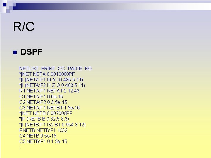
R/C n DSPF NETLIST_PRINT_CC_TWICE: NO *|NET NETA 0. 0010000 PF *|I (NETA: F 1 I 0 A I 0 485. 5 11) *|I (NETA: F 2 I 1 Z O 0 483. 5 11) R 1 NETA: F 2 12. 43 C 1 NETA: F 1 0 6 e-15 C 2 NETA: F 2 0 3. 5 e-15 C 3 NETA: F 1 NETB: F 1 5 e-16 *|NET NETB 0. 007000 PF *|P (NETB B 0 32. 5 8. 3) *|I (NETB: F 1 I 32 B I 0 554. 3 12) RNETB: F 1 1032 C 4 NETB 0 5 e-15 C 5 NETB: F 1 0 1. 5 e-15 :
R/C n RC Extractor ¨ Star-RCXT
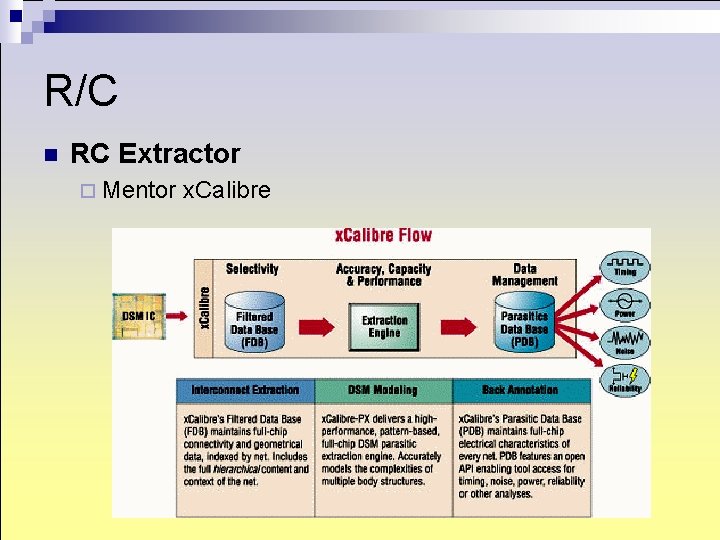
R/C n RC Extractor ¨ Mentor x. Calibre
Outline n n n n Introduction Transistor Process Steps Layout Schematic R/C Design Rules Tools
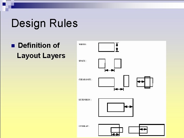
Design Rules n Definition of Layout Layers
Design Rules n Widths 0. 6 um metal 3 0. 3 um metal 2 0. 3 um metal 1 0. 3 um pdiff/ndiff 0. 2 um poly
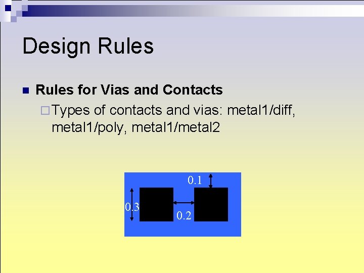
Design Rules for Vias and Contacts ¨ Types of contacts and vias: metal 1/diff, metal 1/poly, metal 1/metal 2 0. 1 0. 3 0. 2
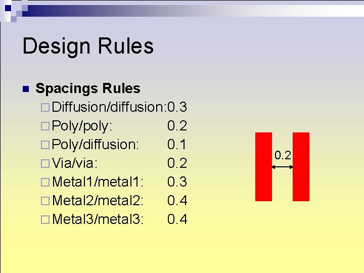
Design Rules n Spacings Rules ¨ Diffusion/diffusion: 0. 3 ¨ Poly/poly: 0. 2 ¨ Poly/diffusion: 0. 1 ¨ Via/via: 0. 2 ¨ Metal 1/metal 1: 0. 3 ¨ Metal 2/metal 2: 0. 4 ¨ Metal 3/metal 3: 0. 4 0. 2
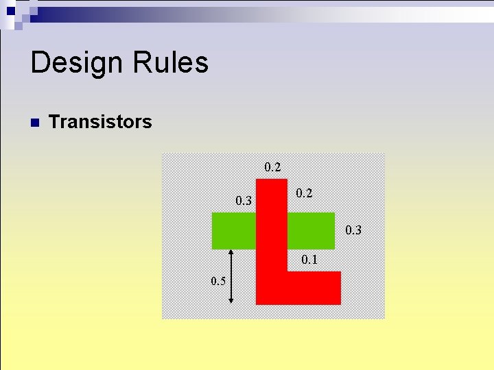
Design Rules n Transistors 0. 2 0. 3 0. 1 0. 5
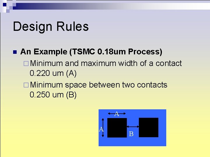
Design Rules n An Example (TSMC 0. 18 um Process) ¨ Minimum and maximum width of a contact 0. 220 um (A) ¨ Minimum space between two contacts 0. 250 um (B) A A B
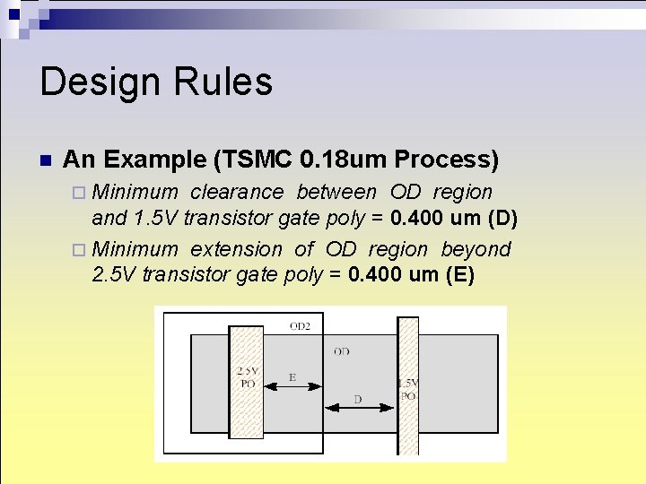
Design Rules n An Example (TSMC 0. 18 um Process) ¨ Minimum clearance between OD region and 1. 5 V transistor gate poly = 0. 400 um (D) ¨ Minimum extension of OD region beyond 2. 5 V transistor gate poly = 0. 400 um (E)
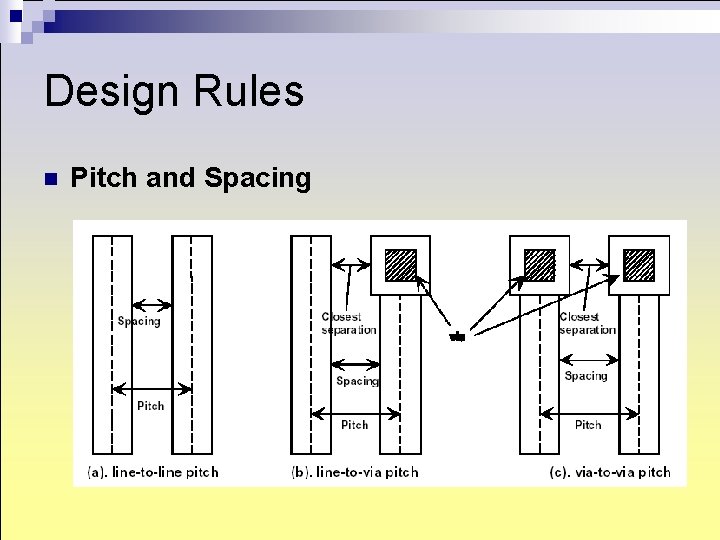
Design Rules n Metal Pitch Consists of Two Parts ¨ The width of the metal line and ¨ The minimum amount of space needed to separate one line from another.
Design Rules n Pitch and Spacing
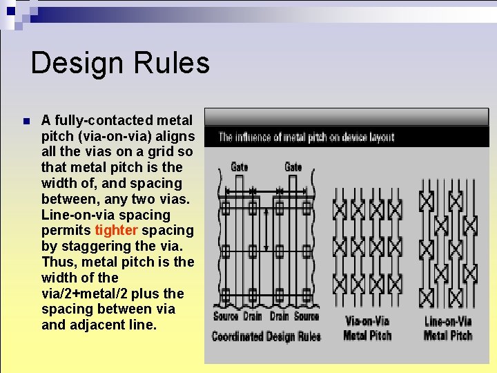
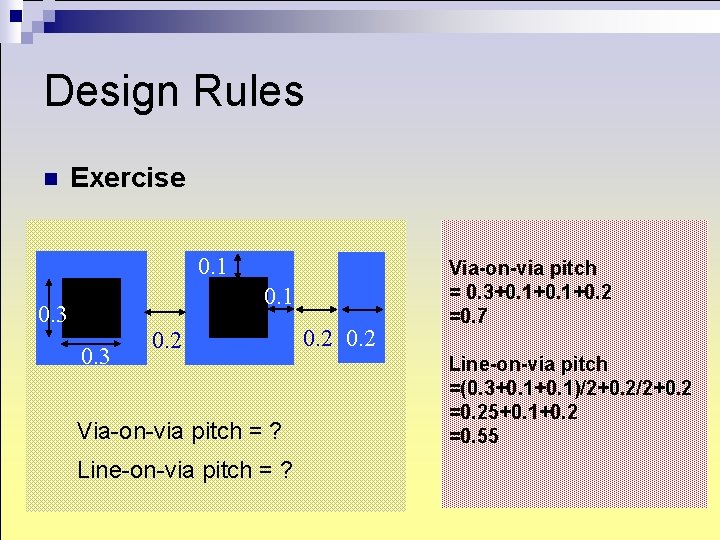
Design Rules n A fully-contacted metal pitch (via-on-via) aligns all the vias on a grid so that metal pitch is the width of, and spacing between, any two vias. Line-on-via spacing permits tighter spacing by staggering the via. Thus, metal pitch is the width of the via/2+metal/2 plus the spacing between via and adjacent line.
Design Rules n Exercise 0. 1 0. 3 0. 2 Via-on-via pitch = ? Line-on-via pitch = ? 0. 2 Via-on-via pitch = 0. 3+0. 1+0. 2 =0. 7 Line-on-via pitch =(0. 3+0. 1)/2+0. 2 =0. 25+0. 1+0. 2 =0. 55
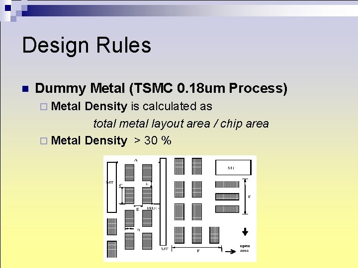
Design Rules n Dummy Metal (TSMC 0. 18 um Process) ¨ Metal Density is calculated as total metal layout area / chip area ¨ Metal Density > 30 %
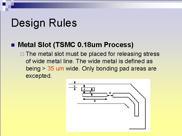
Design Rules n Metal Slot (TSMC 0. 18 um Process) ¨ The metal slot must be placed for releasing stress of wide metal line. The wide metal is defined as being > 35 um wide. Only bonding pad areas are excepted.
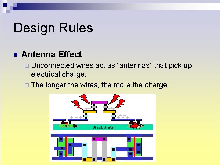
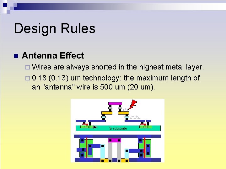
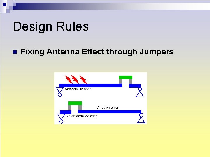
Design Rules n Antenna Effect ¨ Unconnected wires act as “antennas” that pick up electrical charge. ¨ The longer the wires, the more the charge.
Design Rules n Antenna Effect ¨ Wires are always shorted in the highest metal layer. ¨ 0. 18 (0. 13) um technology: the maximum length of an “antenna” wire is 500 um (20 um).
Design Rules n Antenna Effect ¨ Depends on the gate size n Aggressive down sizing makes the problem worse! ¨ Depends on length of the part of the wire that is “unshorted” (that is, not connected to a diffusion drain area)
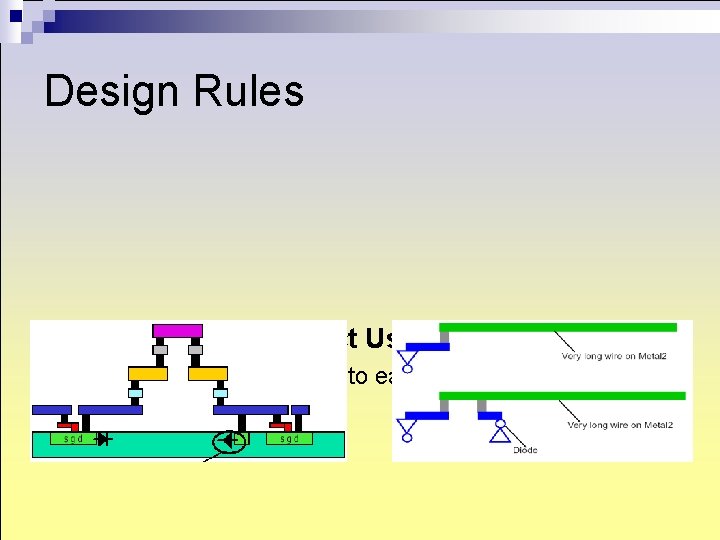
Design Rules n Fixing Antenna Effect Using Diodes ¨ Insert n a diode cell next to each input. Costs significant area
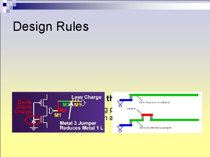
Design Rules n Fixing Antenna Effect through Jumpers ¨ The idea: Force a routing pattern that “shoots up” to the highest layer as soon as possible.
Design Rules n Fixing Antenna Effect through Jumpers
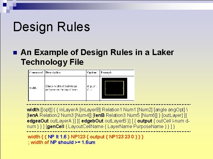
Design Rules n An Example of Design Rules in a Laker Technology File width [[opt]] { { in. Layer. A [in. Layer. B] Relation 1 Num 1 [Num 2] [angle ang. Opt] [len. A Relation 2 Num 3 [Num 4]] [len. B Relation 3 Num 5 [Num 6]] } [out. Layer] [{ edgea. Out out. Layer. A }] [{ edgeb. Out out. Layer. B }] [ { output { out. Cell l-num dnum } } ] [gen. Cell { Layout. Cell. Name { Layer. Name Purpose. Name } } ] } width { { NP lt 1. 6 } NP 123 { output { NP 123 23 0 } } } ; width of NP should >= 1. 6 um
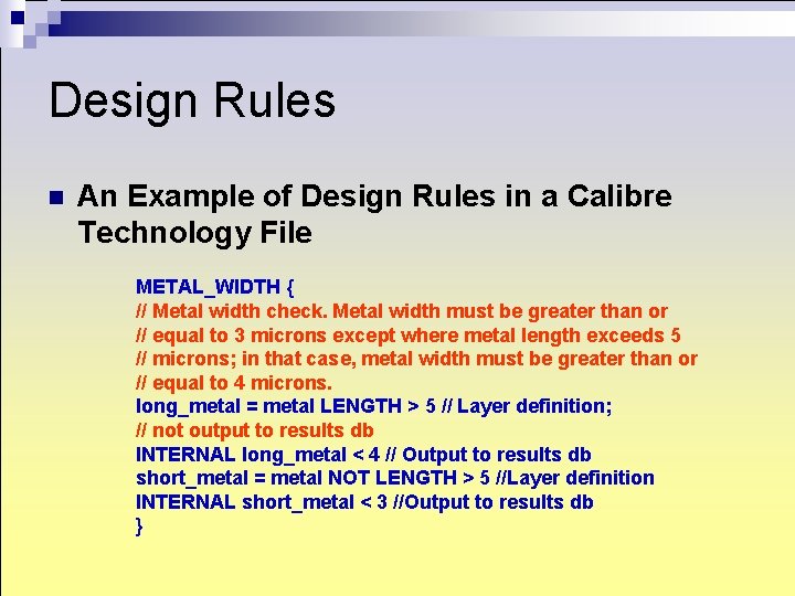
Design Rules n An Example of Design Rules in a Calibre Technology File METAL_WIDTH { // Metal width check. Metal width must be greater than or // equal to 3 microns except where metal length exceeds 5 // microns; in that case, metal width must be greater than or // equal to 4 microns. long_metal = metal LENGTH > 5 // Layer definition; // not output to results db INTERNAL long_metal < 4 // Output to results db short_metal = metal NOT LENGTH > 5 //Layer definition INTERNAL short_metal < 3 //Output to results db }
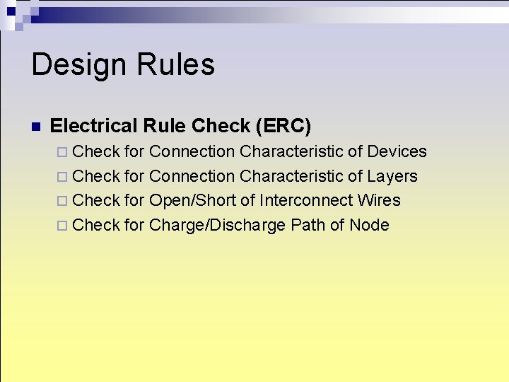
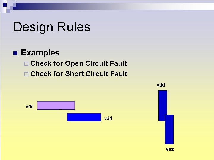
Design Rules n Electrical Rule Check (ERC) ¨ Check for Connection Characteristic of Devices ¨ Check for Connection Characteristic of Layers ¨ Check for Open/Short of Interconnect Wires ¨ Check for Charge/Discharge Path of Node
Design Rules n Examples ¨ Check for Open Circuit Fault ¨ Check for Short Circuit Fault vdd vss
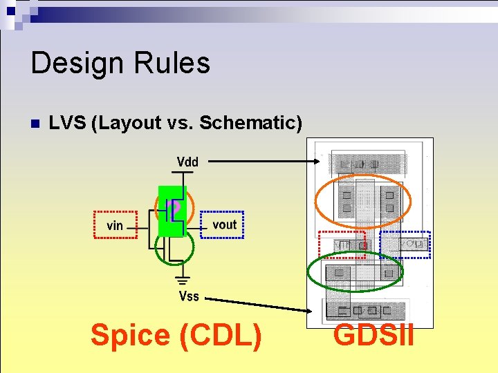
Design Rules n LVS (Layout vs. Schematic) ? Spice (CDL) GDSII
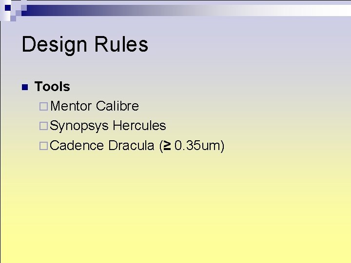
Design Rules n Tools ¨ Mentor Calibre ¨ Synopsys Hercules ¨ Cadence Dracula (≥ 0. 35 um)
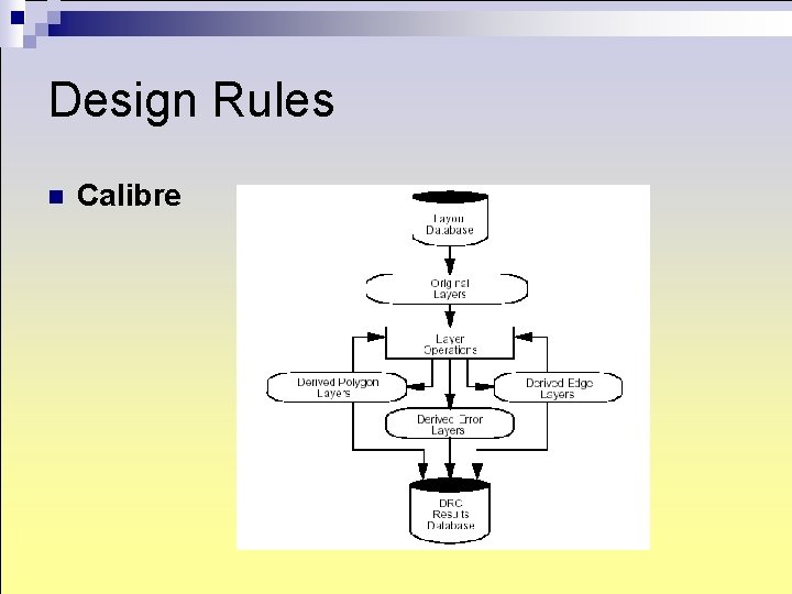
Design Rules n Calibre
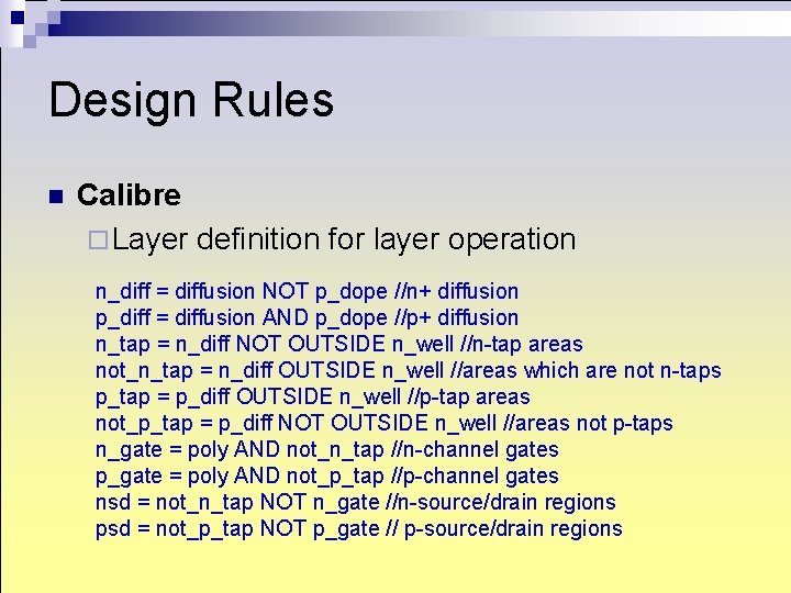
Design Rules n Calibre ¨ Layer definition for layer operation n_diff = diffusion NOT p_dope //n+ diffusion p_diff = diffusion AND p_dope //p+ diffusion n_tap = n_diff NOT OUTSIDE n_well //n-tap areas not_n_tap = n_diff OUTSIDE n_well //areas which are not n-taps p_tap = p_diff OUTSIDE n_well //p-tap areas not_p_tap = p_diff NOT OUTSIDE n_well //areas not p-taps n_gate = poly AND not_n_tap //n-channel gates p_gate = poly AND not_p_tap //p-channel gates nsd = not_n_tap NOT n_gate //n-source/drain regions psd = not_p_tap NOT p_gate // p-source/drain regions
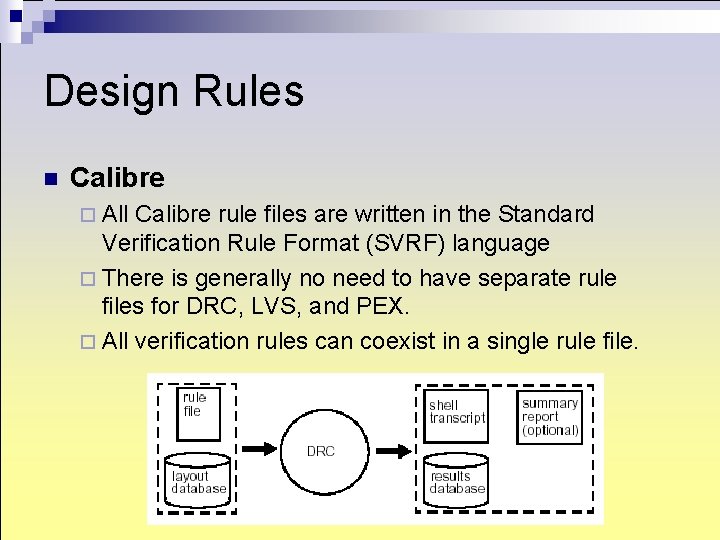
Design Rules n Calibre ¨ All Calibre rule files are written in the Standard Verification Rule Format (SVRF) language ¨ There is generally no need to have separate rule files for DRC, LVS, and PEX. ¨ All verification rules can coexist in a single rule file.
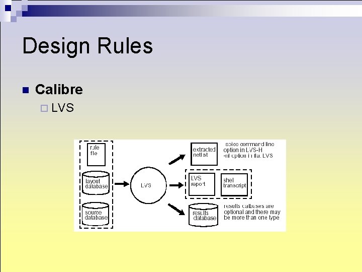
Design Rules n Calibre ¨ LVS
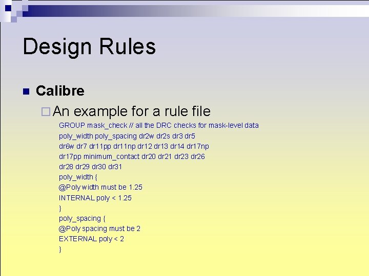
Design Rules n Calibre ¨ An example for a rule file GROUP mask_check // all the DRC checks for mask-level data poly_width poly_spacing dr 2 w dr 2 s dr 3 dr 5 dr 6 w dr 7 dr 11 pp dr 11 np dr 12 dr 13 dr 14 dr 17 np dr 17 pp minimum_contact dr 20 dr 21 dr 23 dr 26 dr 28 dr 29 dr 30 dr 31 poly_width { @Poly width must be 1. 25 INTERNAL poly < 1. 25 } poly_spacing { @Poly spacing must be 2 EXTERNAL poly < 2 }