Layout design rules Introduction Layout rules is also
- Slides: 17

Layout design rules

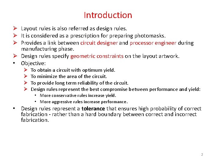
Introduction Ø Layout rules is also referred as design rules. Ø It is considered as a prescription for preparing photomasks. Ø Provides a link between circuit designer and processor engineer during manufacturing phase. Ø Design rules specify geometric constraints on the layout artwork. • Objective: Ø Ø To obtain a circuit with optimum yield. To minimize the area of the circuit. To provide long term reliability of the circuit. Design rules represent the best compromise between performance and yield: • More conservative rules increase yield. • More aggressive rules increase performance. • Design rules represent a tolerance that ensures high probability of correct fabrication - rather than a hard boundary between correct and incorrect fabrication. 2

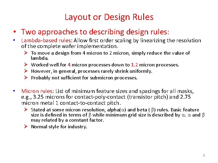
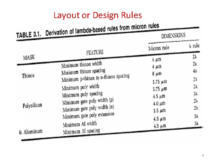
Layout or Design Rules • Two approaches to describing design rules: • Lambda-based rules: Allow first order scaling by linearizing the resolution of the complete wafer implementation. Ø To move a design from 4 micron to 2 micron, simply reduce the value of lambda. Ø Worked well for 4 micron processes down to 1. 2 micron processes. Ø However, in general, processes rarely shrink uniformly. Ø Probably not sufficient for submicron processes. • Micron rules: List of minimum feature sizes and spacings for all masks, e. g. , 3. 25 microns for contact-poly-contact (transistor pitch) and 2. 75 micron metal 1 contact-to-contact pitch. Ø Stated at some micron resolution, alpha( ) and beta ( ) rules. Basic feature size is defined in terms of while minimum grid size is described by . and may related by a constant factor. Ø Normal style for industry. 3

Layout or Design Rules 4

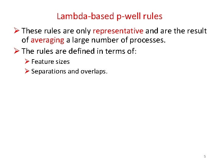
Lambda-based p-well rules Ø These rules are only representative and are the result of averaging a large number of processes. Ø The rules are defined in terms of: Ø Feature sizes Ø Separations and overlaps. 5

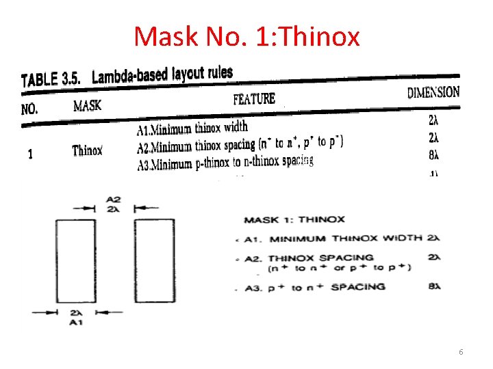
Mask No. 1: Thinox 6

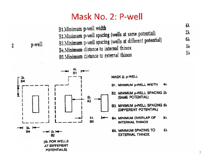
Mask No. 2: P-well 7

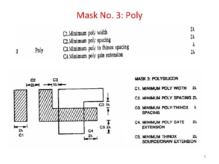
Mask No. 3: Poly 8

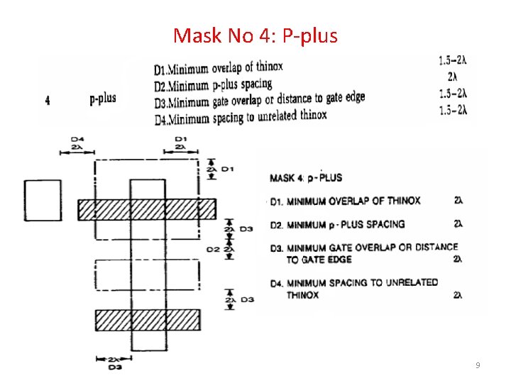
Mask No 4: P-plus 9

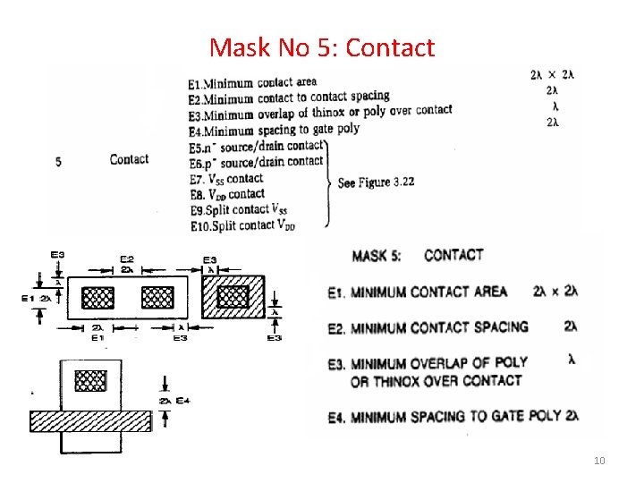
Mask No 5: Contact 10

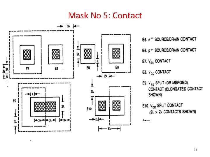
Mask No 5: Contact 11

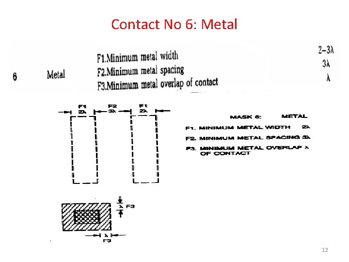
Contact No 6: Metal 12

CMOS Design Rules Ø A layout resembles the top view of the IC Ø The layout design is 2 -dimentional from the viewpoint of an IC designer. Ø in fact, designers normally do not control the depth dimension of an IC. The depth of a transistor source or the thickness of a metal wire is determined by the fabrication process. Ø The layout designer only decides the dimensions and locations of the transistors and interconnects them into the target circuit. Ø The minimum feature size of a technology is typically denoted by the narrowest width of a polysilicon wire that it can produce. Ø For instance, if the narrowest polysilicon wire in a technology is 1 m wide, it is called 1 m technology. Ø Design rules capture the physical limitations of a fabrication process. Ø Design rules release designers from the details of fabrication so they can concentrate on the design instead. 13

CMOS Design Rules Ø In -based design rules (developed by Mead and Conway) the minimum feature size is 2. Ø For a 2 m technology, =1 m Ø Different fabrication technologies apparently require different rules. Ø Drawbacks of scalable design rules: the layout produced according to scalable design rules are often larger than necessary. Ø For example, a minimum spacing of 4 m may be ordered although in reality 3. 2 m is sufficient. 14

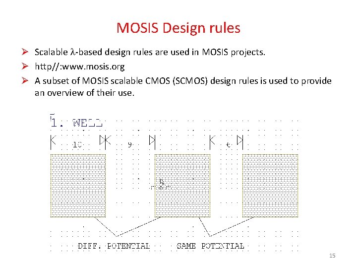
MOSIS Design rules Ø Scalable -based design rules are used in MOSIS projects. Ø http//: www. mosis. org Ø A subset of MOSIS scalable CMOS (SCMOS) design rules is used to provide an overview of their use. 15

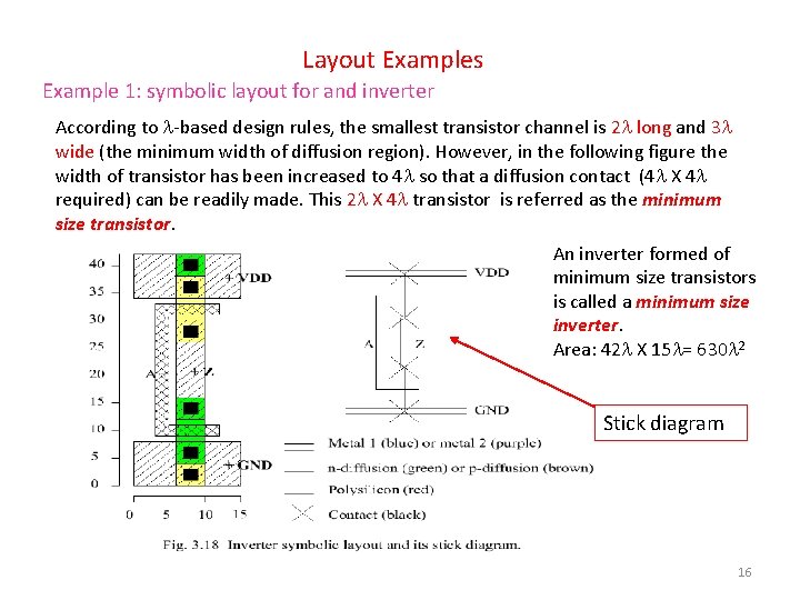
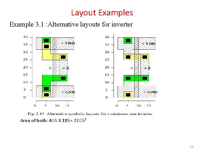
Layout Examples Example 1: symbolic layout for and inverter According to -based design rules, the smallest transistor channel is 2 long and 3 wide (the minimum width of diffusion region). However, in the following figure the width of transistor has been increased to 4 so that a diffusion contact (4 X 4 required) can be readily made. This 2 X 4 transistor is referred as the minimum size transistor. An inverter formed of minimum size transistors is called a minimum size inverter. Area: 42 X 15 = 630 2 Stick diagram 16

Layout Examples Example 3. 1 : Alternative layouts for inverter Area of both: 40 X 18 = 720 2 17