1 VDSM and FullCustom Layout Design Issues1 kyungee

- Slides: 25

1 VDSM and Full-Custom Layout Design Issues(1) 경종민 kyung@ee. kaist. ac. kr

2 Contents • Technology and Foundry Mega-Trend • VDSM (Very Deep Sub-Micron) Issues • Full Custom vs. Standard Cell Layout

3 Technology and Foundry Mega-Trend

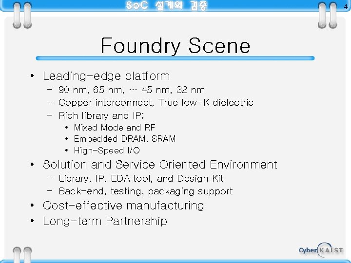
4 Foundry Scene • Leading-edge platform – 90 nm, 65 nm, … 45 nm, 32 nm – Copper interconnect, True low-K dielectric – Rich library and IP; • Mixed Mode and RF • Embedded DRAM, SRAM • High-Speed I/O • Solution and Service Oriented Environment – Library, IP, EDA tool, and Design Kit – Back-end, testing, packaging support • Cost-effective manufacturing • Long-term Partnership

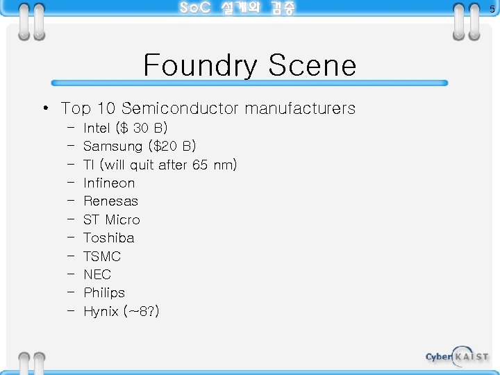
5 Foundry Scene • Top 10 Semiconductor manufacturers – – – Intel ($ 30 B) Samsung ($20 B) TI (will quit after 65 nm) Infineon Renesas ST Micro Toshiba TSMC NEC Philips Hynix (~8? )

6 VDSM (Very Deep Sub. Micron) Issues

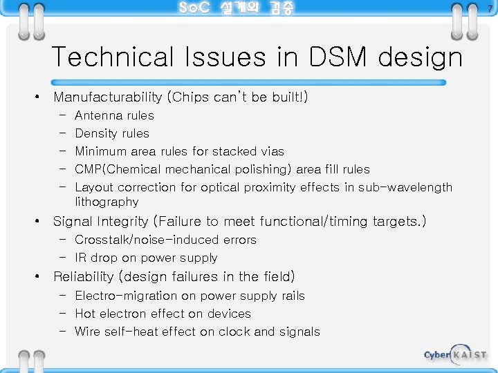
7 Technical Issues in DSM design • Manufacturability (Chips can’t be built!) – – – Antenna rules Density rules Minimum area rules for stacked vias CMP(Chemical mechanical polishing) area fill rules Layout correction for optical proximity effects in sub-wavelength lithography • Signal Integrity (Failure to meet functional/timing targets. ) – Crosstalk/noise-induced errors – IR drop on power supply • Reliability (design failures in the field) – Electro-migration on power supply rails – Hot electron effect on devices – Wire self-heat effect on clock and signals

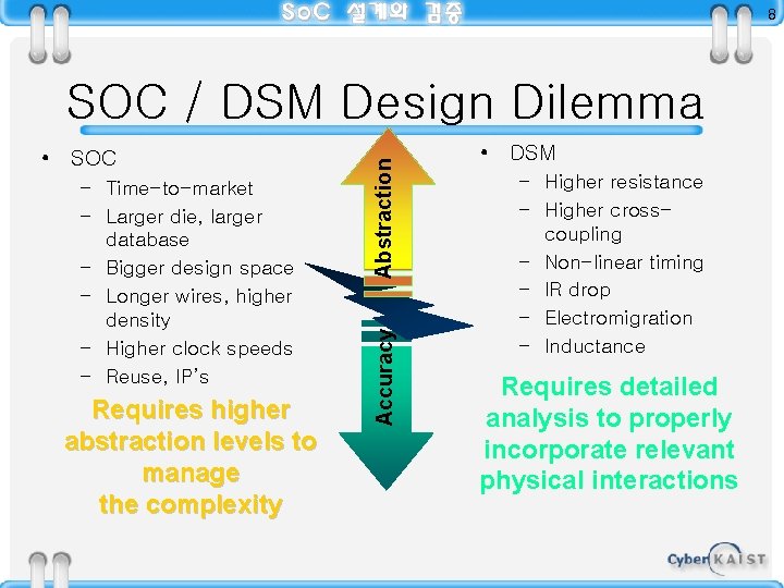
8 – Time-to-market – Larger die, larger database – Bigger design space – Longer wires, higher density – Higher clock speeds – Reuse, IP’s Requires higher abstraction levels to manage the complexity Accuracy • SOC Abstraction SOC / DSM Design Dilemma • DSM – Higher resistance – Higher crosscoupling – Non-linear timing – IR drop – Electromigration – Inductance Requires detailed analysis to properly incorporate relevant physical interactions

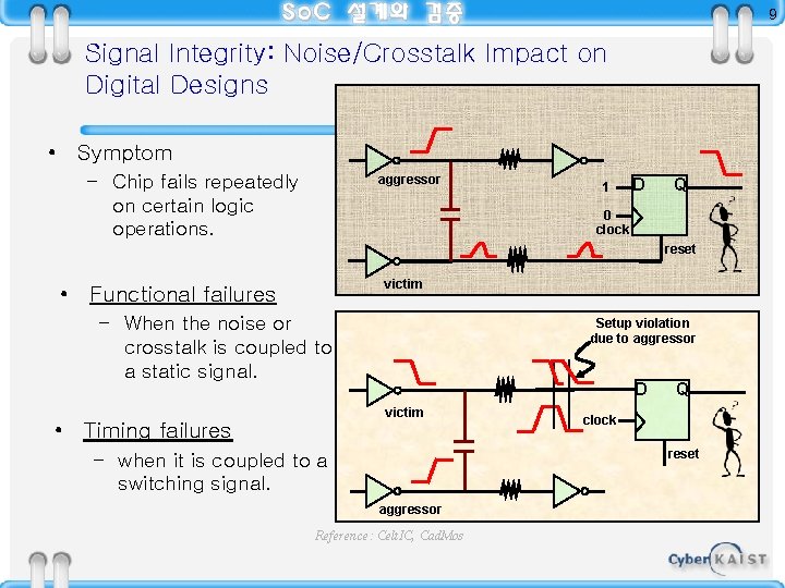
9 Signal Integrity: Noise/Crosstalk Impact on Digital Designs • Symptom – Chip fails repeatedly on certain logic operations. aggressor 1 D Q 0 clock reset victim • Functional failures – When the noise or crosstalk is coupled to a static signal. Setup violation due to aggressor D victim • Timing failures Q clock reset – when it is coupled to a switching signal. aggressor Reference: Celt. IC, Cad. Mos

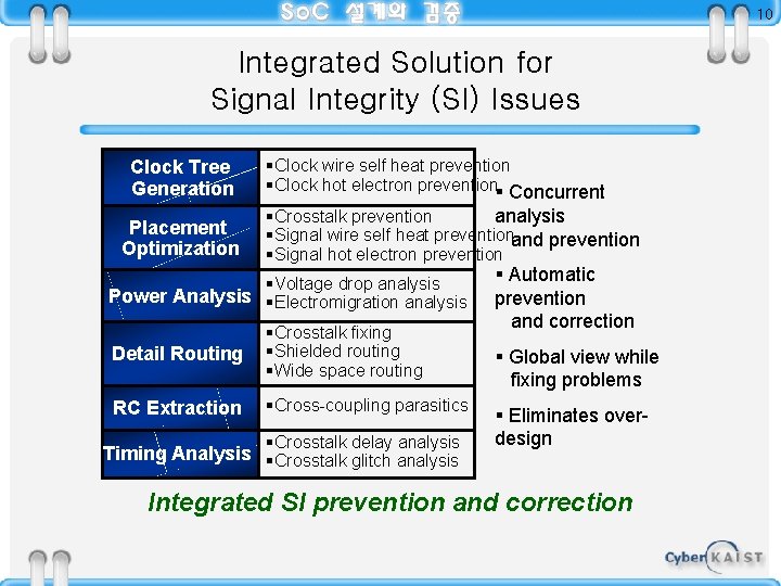
10 Integrated Solution for Signal Integrity (SI) Issues Clock Tree Generation Placement Optimization §Clock wire self heat prevention §Clock hot electron prevention§ Concurrent analysis §Crosstalk prevention §Signal wire self heat preventionand prevention §Signal hot electron prevention §Voltage drop analysis Power Analysis §Electromigration analysis Detail Routing §Crosstalk fixing §Shielded routing §Wide space routing RC Extraction §Cross-coupling parasitics §Crosstalk delay analysis Timing Analysis §Crosstalk glitch analysis § Automatic prevention and correction § Global view while fixing problems § Eliminates overdesign Integrated SI prevention and correction

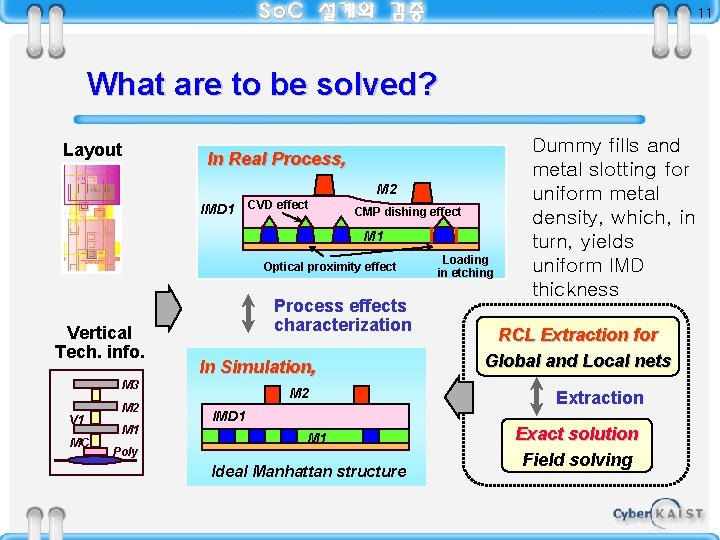
11 What are to be solved? Layout In Real Process, M 2 IMD 1 CVD effect CMP dishing effect M 1 Optical proximity effect Vertical Tech. info. Process effects characterization In Simulation, M 3 V 1 MC M 2 M 1 Poly M 2 IMD 1 M 1 Ideal Manhattan structure Loading in etching Dummy fills and metal slotting for uniform metal density, which, in turn, yields uniform IMD thickness RCL Extraction for Global and Local nets Extraction Exact solution Field solving

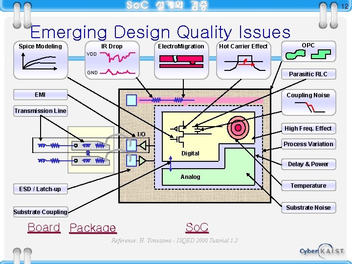
12 Emerging Design Quality Issues Spice Modeling IR Drop Electro. Migration Hot Carrier Effect OPC VDD GND Parasitic RLC EMI Coupling Noise Transmission Line High Freq. Effect I/O Process Variation Digital Delay & Power Analog Temperature ESD / Latch-up Substrate Noise Substrate Coupling Board Package So. C Reference: H. Yonezawa - ISQED 2000 Tutorial 1. 2

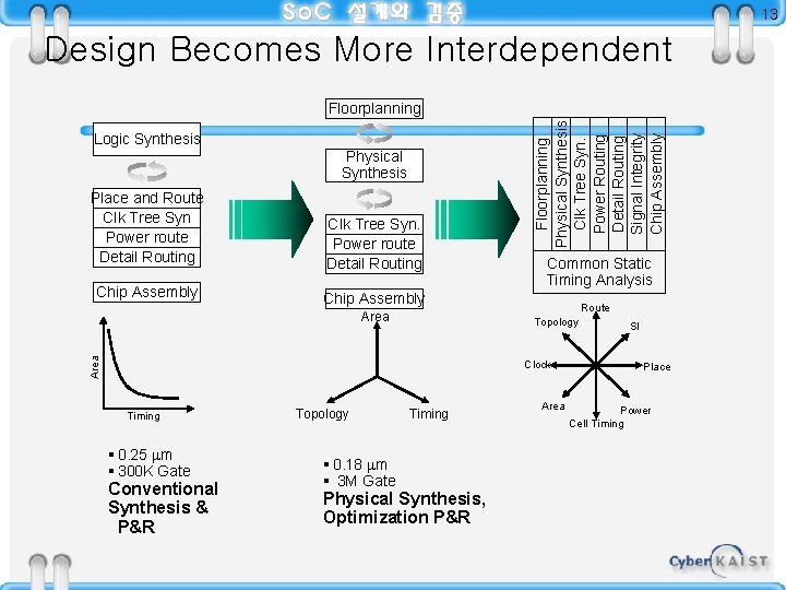
13 Design Becomes More Interdependent Logic Synthesis Physical Synthesis Place and Route Clk Tree Syn Power route Detail Routing Clk Tree Syn. Power route Detail Routing Chip Assembly Area Floorplanning Physical Synthesis Clk Tree Syn. Power Routing Detail Routing Signal Integrity Chip Assembly Floorplanning Common Static Timing Analysis Route Area Topology Clock Timing § 0. 25 mm § 300 K Gate Conventional Synthesis & P&R Topology § 0. 18 mm § 3 M Gate Timing Physical Synthesis, Optimization P&R Area SI Place Power Cell Timing

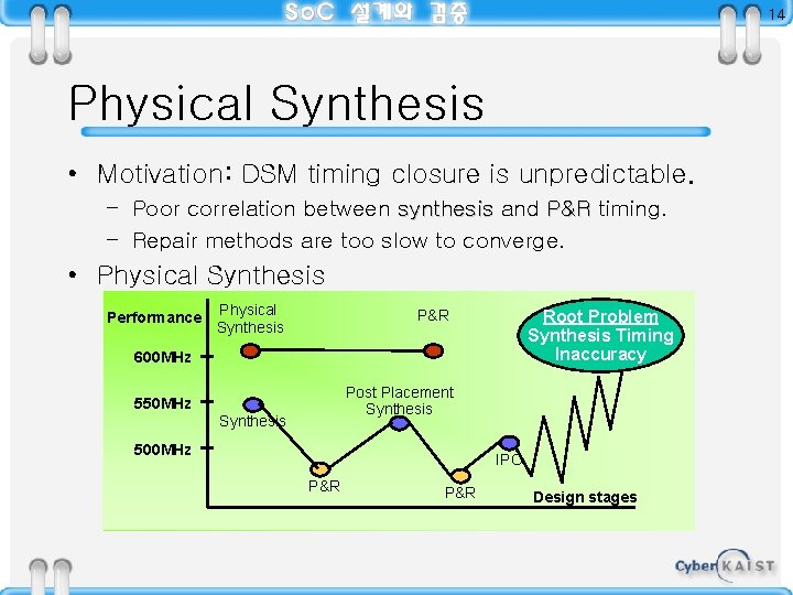
14 Physical Synthesis • Motivation: DSM timing closure is unpredictable. – Poor correlation between synthesis and P&R timing. – Repair methods are too slow to converge. • Physical Synthesis Physical – Physically accurate Performance Synthesis timing in. P&R synthesis – Eliminates iteration 600 MHz – Produces higher performance designs Root Problem Synthesis Timing Inaccuracy Post Placement Synthesis 550 MHz Synthesis 500 MHz IPO P&R Design stages

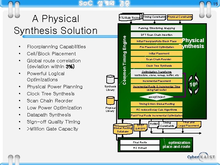
15 A Physical Synthesis Solution • • Floorplanning Capabilities Cell/Block Placement Global route correlation (deviation within 3%) Powerful Logical Optimizations Physical Power Planning Clock Tree Synthesis Scan Chain Reorder Low Power Optimization Datapath Synthesis Sign-off Quality Timing >Million Gate Capacity Timing Constraints Physical Constraints Parsing, Structuring, Mapping Synthesis Library DFT Scan Chain Insertion Common Timing Engine • • • RTL/Gate Source Initial Floorplan/Auto Block Place Pre-Placement Optimization Physical Synthesis Initial Placement Scan Chain Reorder Clock Tree Synthesis Optimization Transforms restructure, clone, remap, buffer, etc Incremental Placement Incremental Route & Incremental Time using fast router 106 accept /reject Timing Driven Global Routing Physical Library RC reduce/Delay Calc Algorithms {Post-Final Route Incremental Optimization} Global Routing Database SPEF D/RSPF Final Route RC Extract Netlist Timing Constraints Final and Legal Placement optimization place-and-route

16 Full Custom vs. Standard Cell Layout

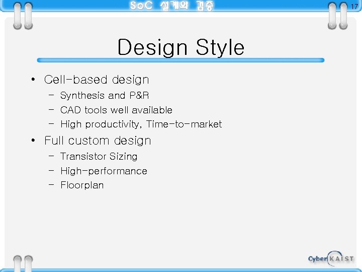
17 Design Style • Cell-based design – Synthesis and P&R – CAD tools well available – High productivity, Time-to-market • Full custom design – Transistor Sizing – High-performance – Floorplan

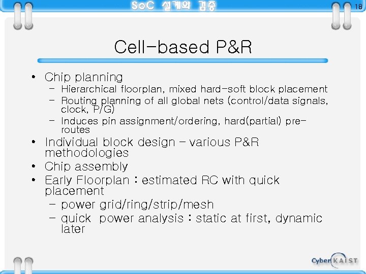
18 Cell-based P&R • Chip planning – Hierarchical floorplan, mixed hard-soft block placement – Routing planning of all global nets (control/data signals, clock, P/G) – Induces pin assignment/ordering, hard(partial) preroutes • Individual block design – various P&R methodologies • Chip assembly • Early Floorplan : estimated RC with quick placement – power grid/ring/strip/mesh – quick power analysis : static at first, dynamic later

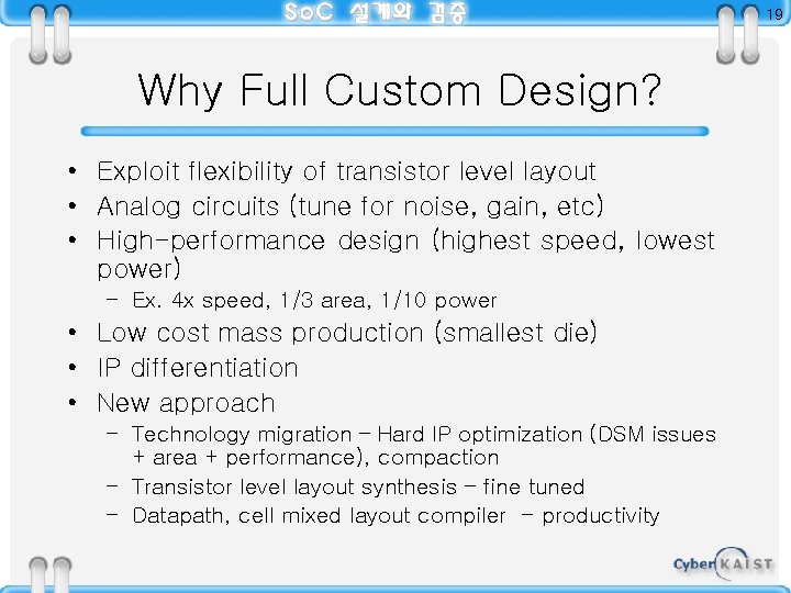
19 Why Full Custom Design? • Exploit flexibility of transistor level layout • Analog circuits (tune for noise, gain, etc) • High-performance design (highest speed, lowest power) – Ex. 4 x speed, 1/3 area, 1/10 power • Low cost mass production (smallest die) • IP differentiation • New approach – Technology migration – Hard IP optimization (DSM issues + area + performance), compaction – Transistor level layout synthesis – fine tuned – Datapath, cell mixed layout compiler - productivity

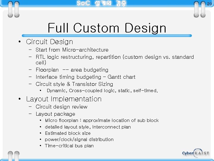
20 Full Custom Design • Circuit Design – Start from Micro-architecture – RTL logic restructuring, repartition (custom design vs. standard cell) – Floorplan -- area budgeting – Interface timing budgeting – Gantt chart – Circuit style & Transistor Sizing • Dynamic, Cross-coupled logic, static, self-timed. • Layout Implementation – Circuit design review – Layout package • • • Micro floorplan : approximate location of sub block detailed layout style, Interconnect plan Estimated block size power/clock/signal distribution Time-critical bus plan

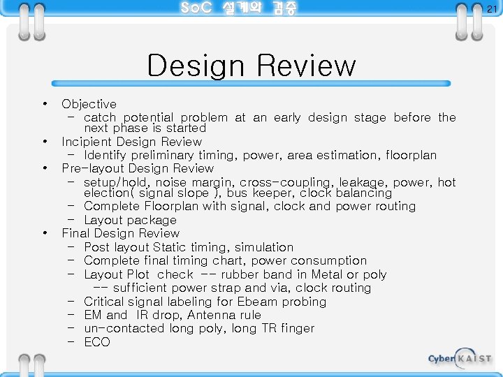
21 Design Review • • Objective – catch potential problem at an early design stage before the next phase is started Incipient Design Review – Identify preliminary timing, power, area estimation, floorplan Pre-layout Design Review – setup/hold, noise margin, cross-coupling, leakage, power, hot election( signal slope ), bus keeper, clock balancing – Complete Floorplan with signal, clock and power routing – Layout package Final Design Review – Post layout Static timing, simulation – Complete final timing chart, power consumption – Layout Plot check -- rubber band in Metal or poly -- sufficient power strap and via, clock routing – Critical signal labeling for Ebeam probing – EM and IR drop, Antenna rule – un-contacted long poly, long TR finger – ECO

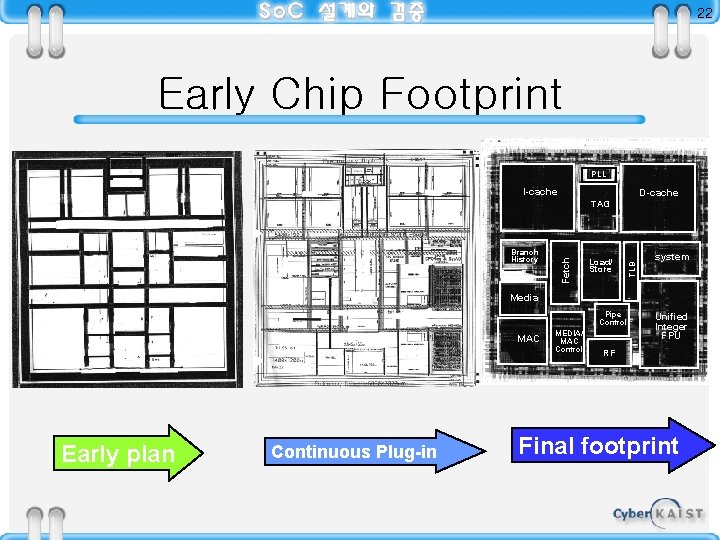
22 Early Chip Footprint PLL I-cache D-cache Load/ Store TLB Branch History Fetch TAG system Media Pipe Control MAC Early plan Continuous Plug-in MEDIA/ MAC Control Unified Integer FPU RF Final footprint

23 Full custom design message • Floorplan ; 설계의 결과가 아니라, 설계의 견인차이 다. – Floorplanning with Interconnect in mind is the only way in DSM design – Core of the FP is ‘ambiguity management’ through area, timing, power budgeting • 270 mm 2 chip이 P&R로 70 mm 2가 되지는 않는다 • 10 MHz설계가 TR size바꾼다고 50 MHz로 동작하지 않는다 • 기존의 설계 결과를 분석해서 정량적인 데이터를 얻음 • Web-based design management system – Task submission/approval/assignment/announcement for critical path reporting, bug reporting/tracking, ECO, etc. all thru. consistent design management system.

24 Floorplan-based ASIC Layout • Objective – Reducing turn-around-time w/o expensive iteration – Early pinpointing the physical design issue at architecture define stage and early feedback – Floorplan-based power and clock distribution – Determining time-critical buffer sizing and Bus/Interconnect planning – Early timing closure – Early attention to deep submicron physical issues and signal integrity

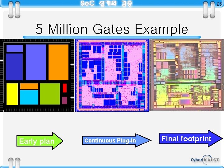
25 5 Million Gates Example Early plan Continuous Plug-in Final footprint