Intel Microelectronics Services VDSM Issues and Design Methodology
![Intel® Microelectronics Services Hot-E Degradation 60 Intel, the Intel logo, and [other trademarks] or Intel® Microelectronics Services Hot-E Degradation 60 Intel, the Intel logo, and [other trademarks] or](https://slidetodoc.com/presentation_image/4e1f36ad53a92152eff69dd703246d07/image-59.jpg)
- Slides: 72

Intel® Microelectronics Services VDSM Issues and Design Methodology January 2002 www. Intel. com/design/ASICs 1 Copyright © 2002 Synopsys, Inc. and Intel Corporation and their licensors. All rights reserved.

Intel Copyright Intel® Microelectronics Services What’s Ahead for Technology Morning Summary 2 Intel, the Intel logo, and [other trademarks] or registered trademarks of the Intel Corporation and its subsidiaries in the United in other countries. *Other. Intel names. Corporation and brands may and be claimed the property of. All others. Copyright ©States 2002 and Synopsys, Inc. and theiraslicensors. rights reserved.

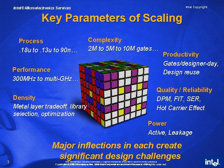
Intel Copyright Intel® Microelectronics Services Key Parameters of Scaling Process. 18 u to. 13 u to 90 n… Complexity 2 M to 5 M to 10 M gates… Performance 300 MHz to multi-GHz… Density Metal layer tradeoff, library selection, optimization Productivity Gates/designer-day, Design reuse Quality / Reliability DPM, FIT, SER, Hot Carrier Effect Power Active, Leakage 3 Major inflections in each create significant design challenges Intel, the Intel logo, and [other trademarks] or registered trademarks of the Intel Corporation and its subsidiaries in the United in other countries. *Other. Intel names. Corporation and brands may and be claimed the property of. All others. Copyright ©States 2002 and Synopsys, Inc. and theiraslicensors. rights reserved.

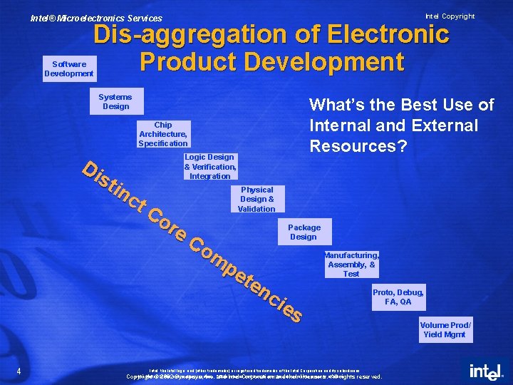
Intel Copyright Intel® Microelectronics Services Dis-aggregation of Electronic Product Development Software Development Systems Design Chip Architecture, Specification Logic Design & Verification, Integration Di st in ct Co re Co m pe te nc i es What’s the Best Use of Internal and External Resources? Physical Design & Validation Package Design 4 Manufacturing, Assembly, & Test Proto, Debug, FA, QA Intel, the Intel logo, and [other trademarks] or registered trademarks of the Intel Corporation and its subsidiaries in the United in other countries. *Other. Intel names. Corporation and brands may and be claimed the property of. All others. Copyright ©States 2002 and Synopsys, Inc. and theiraslicensors. rights reserved. Volume Prod/ Yield Mgmt

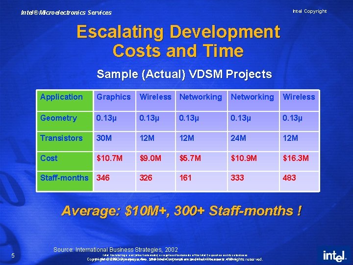
Intel Copyright Intel® Microelectronics Services Escalating Development Costs and Time Sample (Actual) VDSM Projects Application Graphics Wireless Networking Wireless Geometry 0. 13µ Transistors 30 M 12 M 24 M 12 M Cost $10. 7 M $9. 0 M $5. 7 M $10. 9 M $16. 3 M Staff-months 346 326 161 333 483 Average: $10 M+, 300+ Staff-months ! 5 Source: International Business Strategies, 2002 Intel, the Intel logo, and [other trademarks] or registered trademarks of the Intel Corporation and its subsidiaries in the United in other countries. *Other. Intel names. Corporation and brands may and be claimed the property of. All others. Copyright ©States 2002 and Synopsys, Inc. and theiraslicensors. rights reserved.

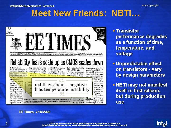
Intel Copyright Intel® Microelectronics Services Meet New Friends: NBTI… § Transistor performance degrades as a function of time, temperature, and voltage § Unpredictable effect on transistors - vary by design parameters § NBTI may not manifest itself in first silicon, but during production use EE Times, 4/15/2002 6 Intel, the Intel logo, and [other trademarks] or registered trademarks of the Intel Corporation and its subsidiaries in the United in other countries. *Other. Intel names. Corporation and brands may and be claimed the property of. All others. Copyright ©States 2002 and Synopsys, Inc. and theiraslicensors. rights reserved.

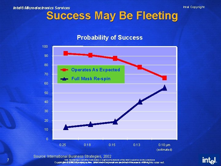
Intel Copyright Intel® Microelectronics Services Success May Be Fleeting Probability of Success 100 90 80 Operates As Expected 70 Full Mask Re-spin 60 50 40 30 20 10 0 0. 25 0. 18 0. 15 0. 13 0. 10 µm (estimated) 7 Source: International Business Strategies, 2002 Intel, the Intel logo, and [other trademarks] or registered trademarks of the Intel Corporation and its subsidiaries in the United in other countries. *Other. Intel names. Corporation and brands may and be claimed the property of. All others. Copyright ©States 2002 and Synopsys, Inc. and theiraslicensors. rights reserved.

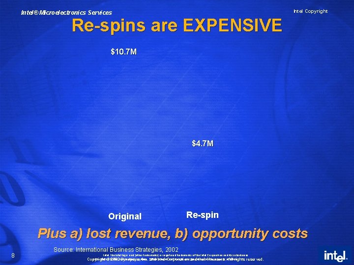
Intel Copyright Intel® Microelectronics Services Re-spins are EXPENSIVE $10. 7 M $4. 7 M Original Re-spin Plus a) lost revenue, b) opportunity costs 8 Source: International Business Strategies, 2002 Intel, the Intel logo, and [other trademarks] or registered trademarks of the Intel Corporation and its subsidiaries in the United in other countries. *Other. Intel names. Corporation and brands may and be claimed the property of. All others. Copyright ©States 2002 and Synopsys, Inc. and theiraslicensors. rights reserved.

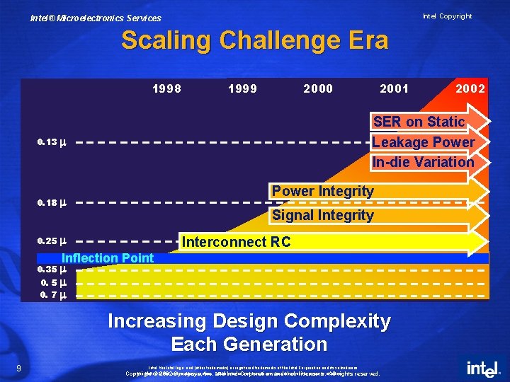
Intel Copyright Intel® Microelectronics Services Scaling Challenge Era 1998 0. 13 m 0. 18 m 0. 25 m 1999 2000 2001 SER on Static Leakage Power In-die Variation Power Integrity Signal Integrity Interconnect RC Inflection Point m 0. 5 m 0. 7 m 0. 35 Increasing Design Complexity Each Generation 9 2002 Intel, the Intel logo, and [other trademarks] or registered trademarks of the Intel Corporation and its subsidiaries in the United in other countries. *Other. Intel names. Corporation and brands may and be claimed the property of. All others. Copyright ©States 2002 and Synopsys, Inc. and theiraslicensors. rights reserved.

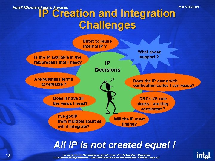
Intel® Microelectronics Services IP Creation and Integration Challenges Intel Copyright Effort to reuse internal IP ? Is the IP available in the fab/process that I need? What about support ? IP Decisions Are business terms acceptable ? Does it have all the views I need? I’ve got IP from multiple sources, will it integrate? Does the IP come with verification suites I can reuse? DRC/LVS rule decks - are they consistent ? Will the IP meet timing? All IP is not created equal ! 10 Intel, the Intel logo, and [other trademarks] or registered trademarks of the Intel Corporation and its subsidiaries in the United in other countries. *Other. Intel names. Corporation and brands may and be claimed the property of. All others. Copyright ©States 2002 and Synopsys, Inc. and theiraslicensors. rights reserved.

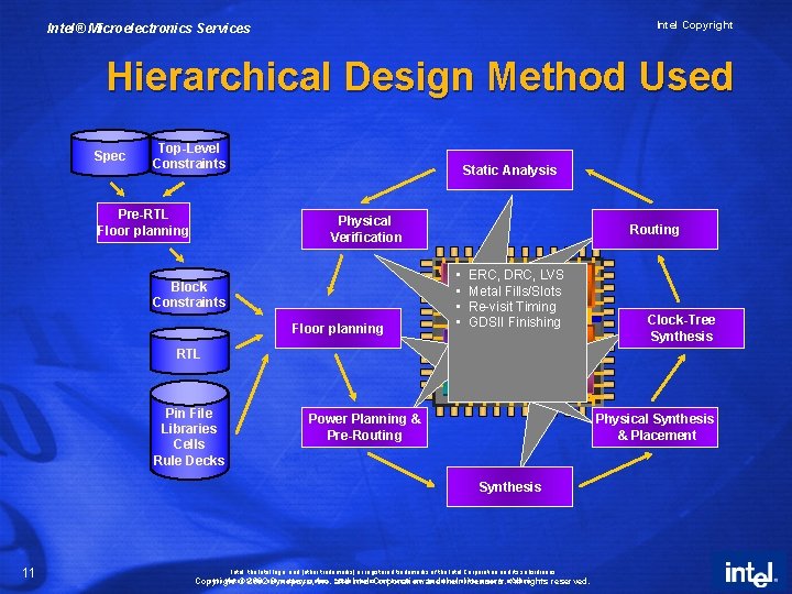
Intel Copyright Intel® Microelectronics Services Hierarchical Design Method Used Spec Top-Level Constraints Pre-RTL Floor planning Static Analysis Physical Verification Block Constraints Floor planning RTL Pin File Libraries Cells Rule Decks Routing • • ERC, I/O Power RTL To Clocking Critical Extraction Placed Placement to. DRC, Analysis Gates Nets Topology Gates LVS Topology Power Connectivity Skew Global, Static Metal mngt Fills/Slots &Bus/Grid Detail Formal Partitioning Clock Congestion Line ECO Without Re-visit delay Pre-routes Timing Crosstalk ctrl Block. Crosstalk Other Timing Fan-out Antennae With GDSII location Pre-routes Finishing Driven ctrl. Fixing Block pin Power andlocation Clocks Obstructions Pre-Routes Refinement Fillers/Spares Scan Re-order Power Planning & Pre-Routing Physical Synthesis & Placement Synthesis 11 Clock-Tree Synthesis Intel, the Intel logo, and [other trademarks] or registered trademarks of the Intel Corporation and its subsidiaries in the United in other countries. *Other. Intel names. Corporation and brands may and be claimed the property of. All others. Copyright ©States 2002 and Synopsys, Inc. and theiraslicensors. rights reserved.

Intel Copyright Intel® Microelectronics Services What’s Ahead High Speed Device Scaling Power Reliability 12 Intel, the Intel logo, and [other trademarks] or registered trademarks of the Intel Corporation and its subsidiaries in the United in other countries. *Other. Intel names. Corporation and brands may and be claimed the property of. All others. Copyright ©States 2002 and Synopsys, Inc. and theiraslicensors. rights reserved.

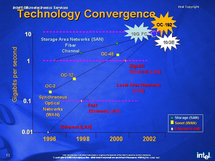
Intel Copyright Intel® Microelectronics Services Technology Convergence OC- 192 Gigabits per second 10 Storage Area Networks (SAN) Fiber Channel OC- 48 10 GE 1 Gigabit Ethernet (LAN) OC- 12 Local Area Networks (LAN) OC-3 0. 1 0. 01 13 10 G- FC Synchronous Optical Networks (WAN) Fast Ethernet( LAN) Storage (SAN) Sonet (WAN) Ethernet (LAN) 1996 1998 Ethernet (LAN) 2000 2002 Intel, the Intel logo, and [other trademarks] or registered trademarks of the Intel Corporation and its subsidiaries in the United in other countries. *Other. Intel names. Corporation and brands may and be claimed the property of. All others. Copyright ©States 2002 and Synopsys, Inc. and theiraslicensors. rights reserved.

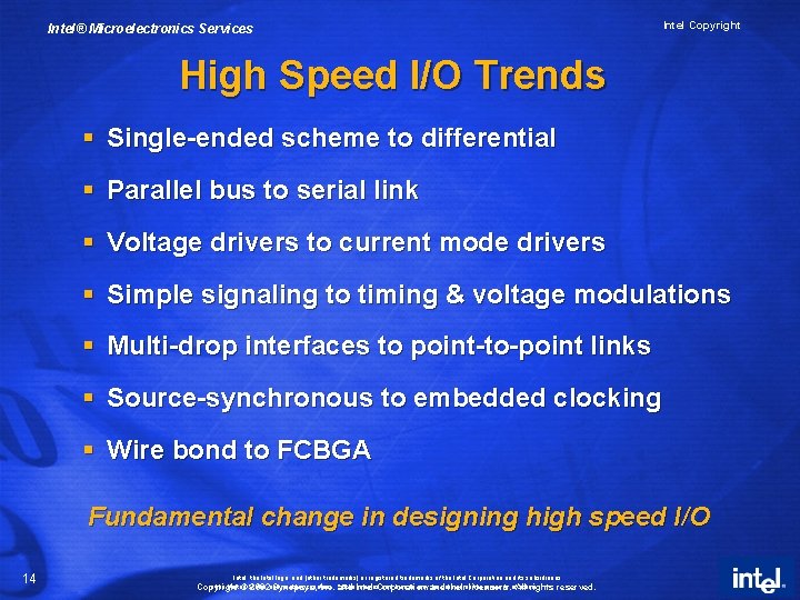
Intel® Microelectronics Services Intel Copyright High Speed I/O Trends § Single-ended scheme to differential § Parallel bus to serial link § Voltage drivers to current mode drivers § Simple signaling to timing & voltage modulations § Multi-drop interfaces to point-to-point links § Source-synchronous to embedded clocking § Wire bond to FCBGA Fundamental change in designing high speed I/O 14 Intel, the Intel logo, and [other trademarks] or registered trademarks of the Intel Corporation and its subsidiaries in the United in other countries. *Other. Intel names. Corporation and brands may and be claimed the property of. All others. Copyright ©States 2002 and Synopsys, Inc. and theiraslicensors. rights reserved.

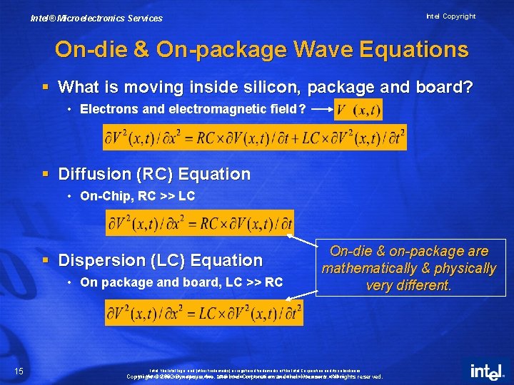
Intel Copyright Intel® Microelectronics Services On-die & On-package Wave Equations § What is moving inside silicon, package and board? • Electrons and electromagnetic field ? § Diffusion (RC) Equation • On-Chip, RC >> LC § Dispersion (LC) Equation • On package and board, LC >> RC 15 On-die & on-package are mathematically & physically very different. Intel, the Intel logo, and [other trademarks] or registered trademarks of the Intel Corporation and its subsidiaries in the United in other countries. *Other. Intel names. Corporation and brands may and be claimed the property of. All others. Copyright ©States 2002 and Synopsys, Inc. and theiraslicensors. rights reserved.

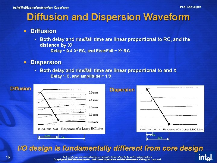
Intel Copyright Intel® Microelectronics Services Diffusion and Dispersion Waveform § Diffusion • Both delay and rise/fall time are linear proportional to RC, and the distance by X 2 Delay ~ 0. 4 X 2 RC, and Rise/Fall ~ X 2 RC § Dispersion • Both delay and rise/fall time are linear proportional to and X Delay ~ X, and amplitude ~ 1/X Diffusion Dispersion 0. 8 ns 2 ns 4 m 20 m I/O design is fundamentally different from core design 16 Intel, the Intel logo, and [other trademarks] or registered trademarks of the Intel Corporation and its subsidiaries in the United in other countries. *Other. Intel names. Corporation and brands may and be claimed the property of. All others. Copyright ©States 2002 and Synopsys, Inc. and theiraslicensors. rights reserved.

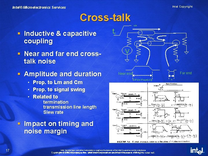
Intel Copyright Intel® Microelectronics Services Cross-talk vin § Inductive & capacitive coupling § Near and far end crosstalk noise § Amplitude and duration • Prop. to Lm and Cm • Prop. to signal swing • Related to tr V Far end Near end 0. 5*(tr+X*sqrt(LC)) termination transmission line length Slew rate § Impact on timing and noise margin 17 Scan – more cases Intel, the Intel logo, and [other trademarks] or registered trademarks of the Intel Corporation and its subsidiaries in the United in other countries. *Other. Intel names. Corporation and brands may and be claimed the property of. All others. Copyright ©States 2002 and Synopsys, Inc. and theiraslicensors. rights reserved. tr

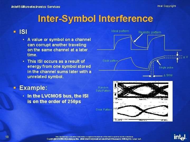
Intel Copyright Intel® Microelectronics Services Inter-Symbol Interference § ISI Ideal pattern Realistic pattern • A value or symbol on a channel can corrupt another traveling on the same channel at a later time. • This ISI occurs as a result of energy from one symbol stored in the channel sums later with a unrelated symbol. § Example: DV Clock pattern Single pulse D time Random Data Pattern • In the LVCMOS bus, the ISI is on the order of 250 ps Clock Pattern 18 Scan - Data an clock pattern Intel, the Intel logo, and [other trademarks] or registered trademarks of the Intel Corporation and its subsidiaries in the United in other countries. *Other. Intel names. Corporation and brands may and be claimed the property of. All others. Copyright ©States 2002 and Synopsys, Inc. and theiraslicensors. rights reserved.

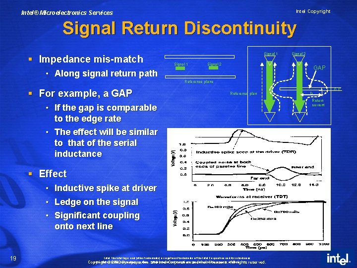
Intel Copyright Intel® Microelectronics Services Signal Return Discontinuity § Impedance mis-match Signal 1 Signal 2 GAP • Along signal return path Reference plane § For example, a GAP Reference plan Return current • If the gap is comparable to the edge rate • The effect will be similar to that of the serial inductance § Effect • Inductive spike at driver • Ledge on the signal • Significant coupling onto next line 19 D Scan - Intel, the Intel logo, and [other trademarks] or registered trademarks of the Intel Corporation and its subsidiaries in the United in other countries. *Other. Intel names. Corporation and brands may and be claimed the property of. All others. Copyright ©States 2002 and Synopsys, Inc. and theiraslicensors. rights reserved. 0. 1”

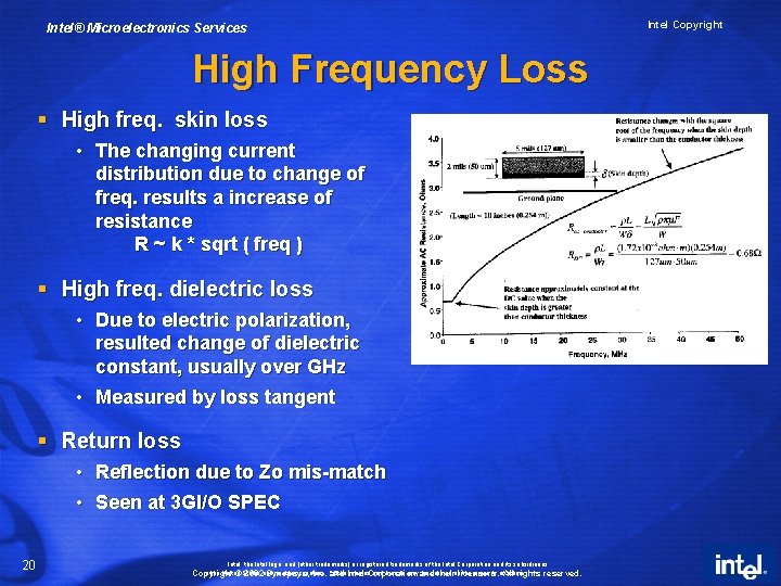
Intel Copyright Intel® Microelectronics Services High Frequency Loss § High freq. skin loss • The changing current distribution due to change of freq. results a increase of resistance R ~ k * sqrt ( freq ) Scan picture § High freq. dielectric loss • Due to electric polarization, resulted change of dielectric constant, usually over GHz • Measured by loss tangent § Return loss • Reflection due to Zo mis-match • Seen at 3 GI/O SPEC 20 Intel, the Intel logo, and [other trademarks] or registered trademarks of the Intel Corporation and its subsidiaries in the United in other countries. *Other. Intel names. Corporation and brands may and be claimed the property of. All others. Copyright ©States 2002 and Synopsys, Inc. and theiraslicensors. rights reserved.

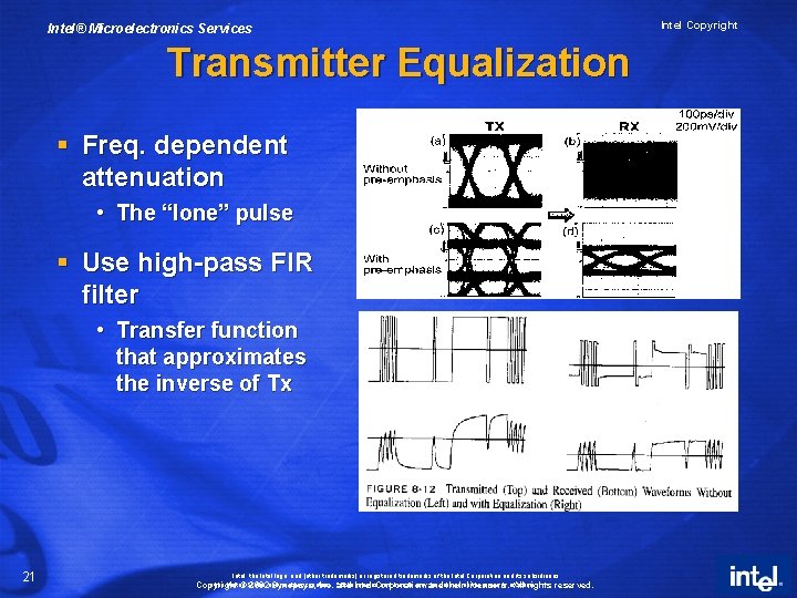
Intel® Microelectronics Services Transmitter Equalization § Freq. dependent attenuation • The “lone” pulse § Use high-pass FIR filter • Transfer function that approximates the inverse of Tx 21 Intel, the Intel logo, and [other trademarks] or registered trademarks of the Intel Corporation and its subsidiaries in the United in other countries. *Other. Intel names. Corporation and brands may and be claimed the property of. All others. Copyright ©States 2002 and Synopsys, Inc. and theiraslicensors. rights reserved. Intel Copyright

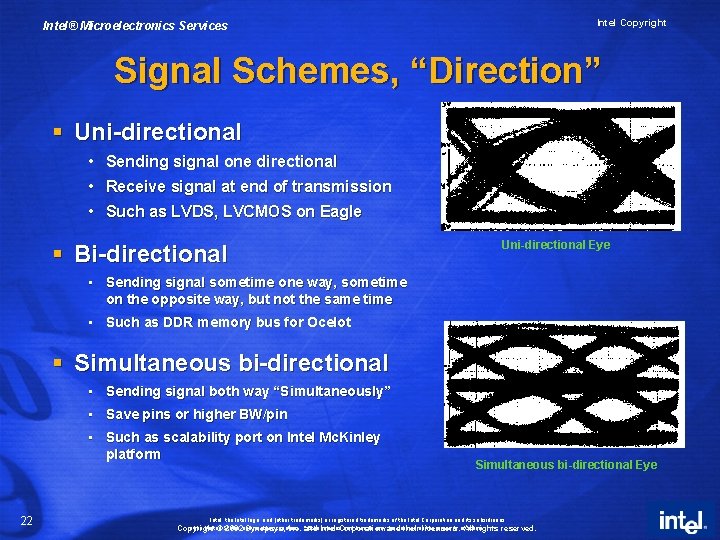
Intel Copyright Intel® Microelectronics Services Signal Schemes, “Direction” § Uni-directional • Sending signal one directional • Receive signal at end of transmission • Such as LVDS, LVCMOS on Eagle § Bi-directional Uni-directional Eye • Sending signal sometime one way, sometime on the opposite way, but not the same time • Such as DDR memory bus for Ocelot § Simultaneous bi-directional • Sending signal both way “Simultaneously” • Save pins or higher BW/pin • Such as scalability port on Intel Mc. Kinley platform 22 Simultaneous bi-directional Eye Intel, the Intel logo, and [other trademarks] or registered trademarks of the Intel Corporation and its subsidiaries in the United in other countries. *Other. Intel names. Corporation and brands may and be claimed the property of. All others. Copyright ©States 2002 and Synopsys, Inc. and theiraslicensors. rights reserved.

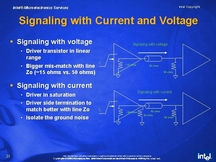
Intel Copyright Intel® Microelectronics Services Signaling with Current and Voltage § Signaling with voltage • Driver transistor in linear range • Bigger mis-match with line Zo (~15 ohms vs. 50 ohms) Signaling with voltage tr ~ 15 ohms 50 ohms § Signaling with current • Driver in saturation • Driver side termination to match better with line Zo • Isolate the ground noise 23 Signaling with current tr >300 ohms 50 ohms Intel, the Intel logo, and [other trademarks] or registered trademarks of the Intel Corporation and its subsidiaries in the United in other countries. *Other. Intel names. Corporation and brands may and be claimed the property of. All others. Copyright ©States 2002 and Synopsys, Inc. and theiraslicensors. rights reserved. 50 ohms

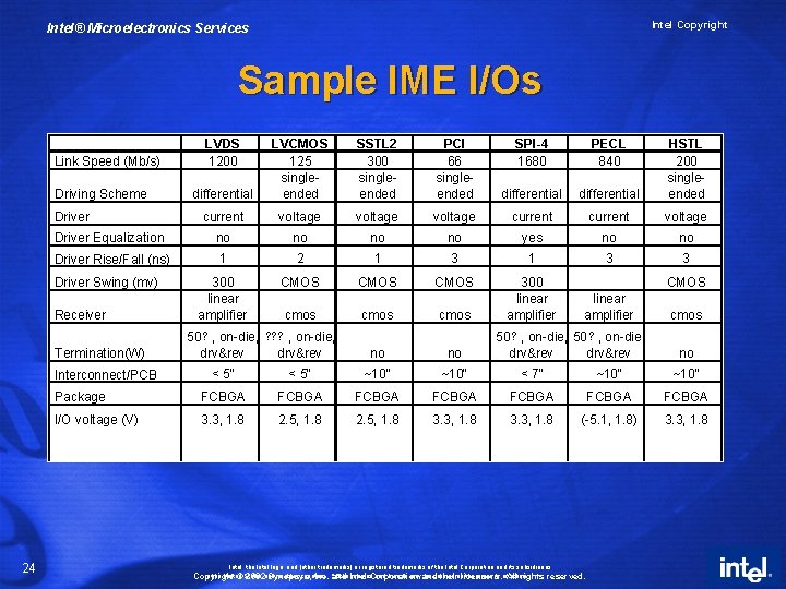
Intel Copyright Intel® Microelectronics Services Sample IME I/Os SSTL 2 300 singleended PCI 66 singleended SPI-4 1680 PECL 840 differential LVCMOS 125 singleended differential HSTL 200 singleended current voltage current voltage Driver Equalization no no yes no no Driver Rise/Fall (ns) 1 2 1 3 3 300 linear amplifier CMOS 300 linear amplifier Link Speed (Mb/s) Driving Scheme Driver Swing (mv) Receiver Termination(W) cmos 50 ? , on-die, ? ? ? , on-die, drv&rev cmos no no CMOS linear amplifier 50 ? , on-die, drv&rev cmos no < 5" ~10" < 7" ~10" Package FCBGA FCBGA I/O voltage (V) 3. 3, 1. 8 2. 5, 1. 8 3. 3, 1. 8 (-5. 1, 1. 8) 3. 3, 1. 8 Interconnect/PCB 24 LVDS 1200 Intel, the Intel logo, and [other trademarks] or registered trademarks of the Intel Corporation and its subsidiaries in the United in other countries. *Other. Intel names. Corporation and brands may and be claimed the property of. All others. Copyright ©States 2002 and Synopsys, Inc. and theiraslicensors. rights reserved.

Intel Copyright Intel® Microelectronics Services What’s Ahead High Speed Device Scaling Power Reliability 25 Intel, the Intel logo, and [other trademarks] or registered trademarks of the Intel Corporation and its subsidiaries in the United in other countries. *Other. Intel names. Corporation and brands may and be claimed the property of. All others. Copyright ©States 2002 and Synopsys, Inc. and theiraslicensors. rights reserved.

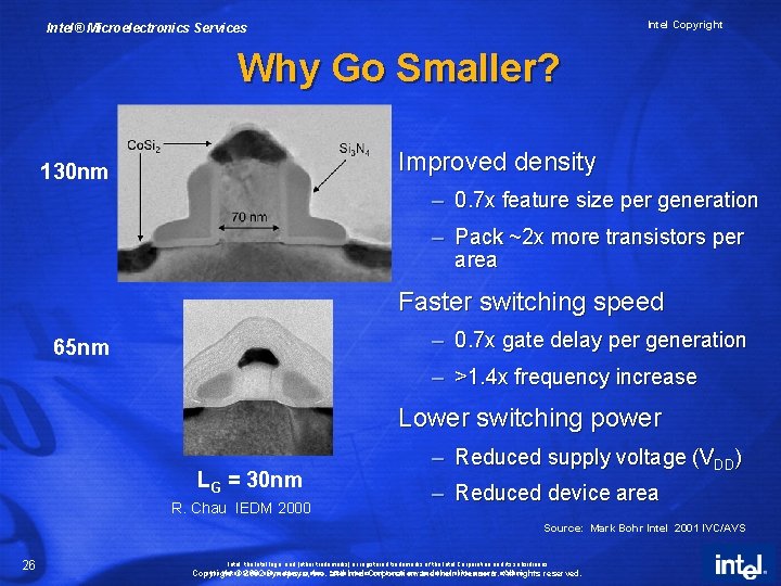
Intel Copyright Intel® Microelectronics Services Why Go Smaller? Improved density 130 nm – 0. 7 x feature size per generation – Pack ~2 x more transistors per area Faster switching speed – 0. 7 x gate delay per generation 65 nm – >1. 4 x frequency increase Lower switching power LG = 30 nm R. Chau IEDM 2000 – Reduced supply voltage (VDD) – Reduced device area Source: Mark Bohr Intel 2001 IVC/AVS 26 Intel, the Intel logo, and [other trademarks] or registered trademarks of the Intel Corporation and its subsidiaries in the United in other countries. *Other. Intel names. Corporation and brands may and be claimed the property of. All others. Copyright ©States 2002 and Synopsys, Inc. and theiraslicensors. rights reserved.

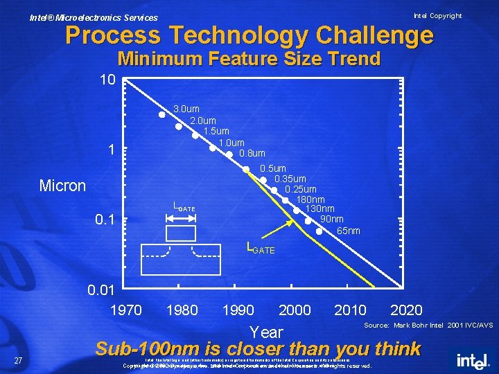
Intel Copyright Intel® Microelectronics Services Process Technology Challenge Minimum Feature Size Trend 10 3. 0 um 2. 0 um 1. 5 um 1. 0 um 0. 8 um 1 0. 5 um 0. 35 um 0. 25 um 180 nm 130 nm 90 nm 65 nm Micron LGATE 0. 1 LGATE 0. 01 1970 1980 1990 2000 2010 Year 27 2020 Source: Mark Bohr Intel 2001 IVC/AVS Sub-100 nm is closer than you think Intel, the Intel logo, and [other trademarks] or registered trademarks of the Intel Corporation and its subsidiaries in the United in other countries. *Other. Intel names. Corporation and brands may and be claimed the property of. All others. Copyright ©States 2002 and Synopsys, Inc. and theiraslicensors. rights reserved.

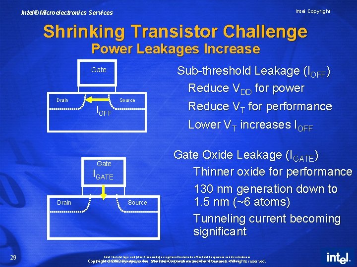
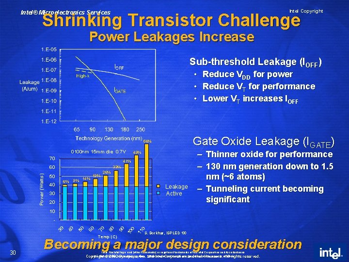
Intel Copyright Intel® Microelectronics Services Shrinking Transistor Challenge Power Leakages Increase Sub-threshold Leakage (IOFF) Reduce VDD for power Gate Drain Source IOFF Reduce VT for performance Lower VT increases IOFF Gate IGATE Drain 29 Source Gate Oxide Leakage (IGATE) Thinner oxide for performance 130 nm generation down to 1. 5 nm (~6 atoms) Tunneling current becoming significant Intel, the Intel logo, and [other trademarks] or registered trademarks of the Intel Corporation and its subsidiaries in the United in other countries. *Other. Intel names. Corporation and brands may and be claimed the property of. All others. Copyright ©States 2002 and Synopsys, Inc. and theiraslicensors. rights reserved.

Intel Copyright Intel® Microelectronics Services Shrinking Transistor Challenge Power Leakages Increase Sub-threshold Leakage (IOFF) • • • Gate Oxide Leakage (IGATE) 56% 0100 nm 15 mm die 0. 7 V 70 Power (Watts) 49% 41% 60 33% 50 6% 40 9% 14% 19% 26% Leakage Active 30 Reduce VDD for power Reduce VT for performance Lower VT increases IOFF 20 – Thinner oxide for performance – 130 nm generation down to 1. 5 nm (~6 atoms) – Tunneling current becoming significant 10 30 0 11 0 Temp (C) 10 90 80 70 60 50 40 30 S. Borkhar, ISPLED ‘ 00 Becoming a major design consideration Intel, the Intel logo, and [other trademarks] or registered trademarks of the Intel Corporation and its subsidiaries in the United in other countries. *Other. Intel names. Corporation and brands may and be claimed the property of. All others. Copyright ©States 2002 and Synopsys, Inc. and theiraslicensors. rights reserved.

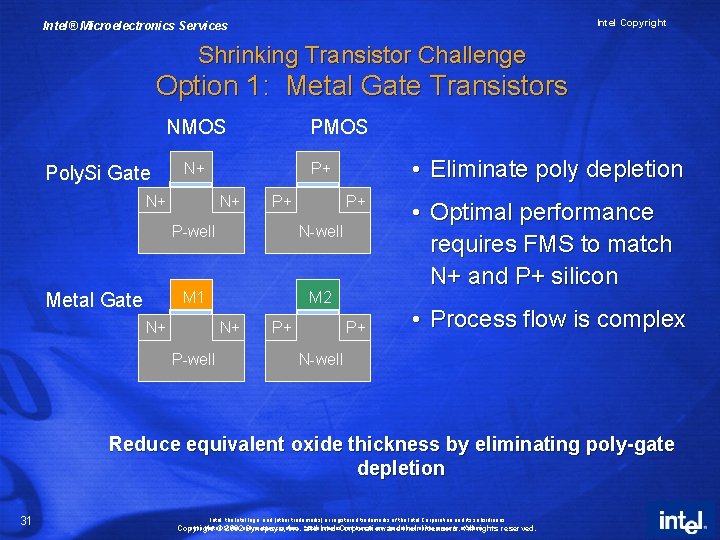
Intel Copyright Intel® Microelectronics Services Shrinking Transistor Challenge Option 1: Metal Gate Transistors NMOS Poly. Si Gate N+ • Eliminate poly depletion P+ N+ Metal Gate PMOS N+ P+ P+ P-well N-well M 1 M 2 N+ N+ P-well P+ P+ • Optimal performance requires FMS to match N+ and P+ silicon • Process flow is complex N-well Reduce equivalent oxide thickness by eliminating poly-gate depletion 31 Intel, the Intel logo, and [other trademarks] or registered trademarks of the Intel Corporation and its subsidiaries in the United in other countries. *Other. Intel names. Corporation and brands may and be claimed the property of. All others. Copyright ©States 2002 and Synopsys, Inc. and theiraslicensors. rights reserved.

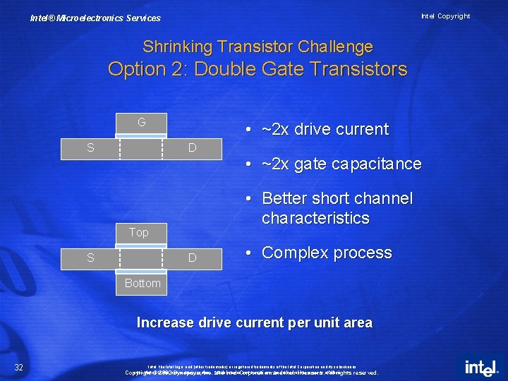
Intel Copyright Intel® Microelectronics Services Shrinking Transistor Challenge Option 2: Double Gate Transistors G • ~2 x drive current S D • Better short channel characteristics Top S • ~2 x gate capacitance D • Complex process Bottom Increase drive current per unit area 32 Intel, the Intel logo, and [other trademarks] or registered trademarks of the Intel Corporation and its subsidiaries in the United in other countries. *Other. Intel names. Corporation and brands may and be claimed the property of. All others. Copyright ©States 2002 and Synopsys, Inc. and theiraslicensors. rights reserved.

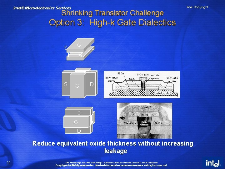
Intel® Microelectronics Services Shrinking Transistor Challenge Intel Copyright Option 3: High-k Gate Dialectics S S G G D D S G D Reduce equivalent oxide thickness without increasing leakage 33 Intel, the Intel logo, and [other trademarks] or registered trademarks of the Intel Corporation and its subsidiaries in the United in other countries. *Other. Intel names. Corporation and brands may and be claimed the property of. All others. Copyright ©States 2002 and Synopsys, Inc. and theiraslicensors. rights reserved.

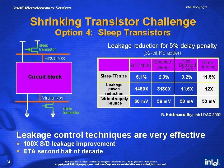
Intel Copyright Intel® Microelectronics Services Shrinking Transistor Challenge Option 4: Sleep Transistors Leakage reduction for 5% delay penalty sleep transistor (32 -bit KS adder) Virtual Vcc Boosted MTCMOS Sleep Circuit block Sleep-TR size Leakage power reduction Virtual supply bounce Virtual Vss Non. Boosted Sleep Stackforcing 5. 1% 2. 3% 3. 2% 11. 5% 1450 X 3130 X 11. 5 X 12 X 60 m. V 59 m. V 58 m. V 50 m. V sleep transistor R. Krishnamurthy, Intel DAC 2002 Leakage control techniques are very effective § 100 X S/D leakage improvement § ETA second half of decade 34 Intel, the Intel logo, and [other trademarks] or registered trademarks of the Intel Corporation and its subsidiaries in the United in other countries. *Other. Intel names. Corporation and brands may and be claimed the property of. All others. Copyright ©States 2002 and Synopsys, Inc. and theiraslicensors. rights reserved.

Intel Copyright Intel® Microelectronics Services The 10, 000 Foot View § 100 nm introduces a whole new world of issues • The days of simple device scaling are over • Process technology will continue to drive to smaller geometries § New approaches, structures, design methods and flows are needed to meet scaling challenges 35 Intel, the Intel logo, and [other trademarks] or registered trademarks of the Intel Corporation and its subsidiaries in the United in other countries. *Other. Intel names. Corporation and brands may and be claimed the property of. All others. Copyright ©States 2002 and Synopsys, Inc. and theiraslicensors. rights reserved.

Intel Copyright Intel® Microelectronics Services What’s Ahead High Speed Device Scaling Power Reliability 36 Intel, the Intel logo, and [other trademarks] or registered trademarks of the Intel Corporation and its subsidiaries in the United in other countries. *Other. Intel names. Corporation and brands may and be claimed the property of. All others. Copyright ©States 2002 and Synopsys, Inc. and theiraslicensors. rights reserved.

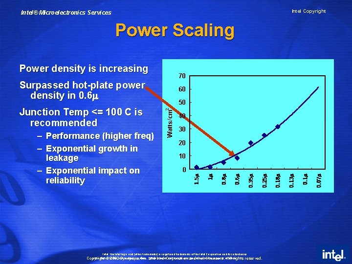
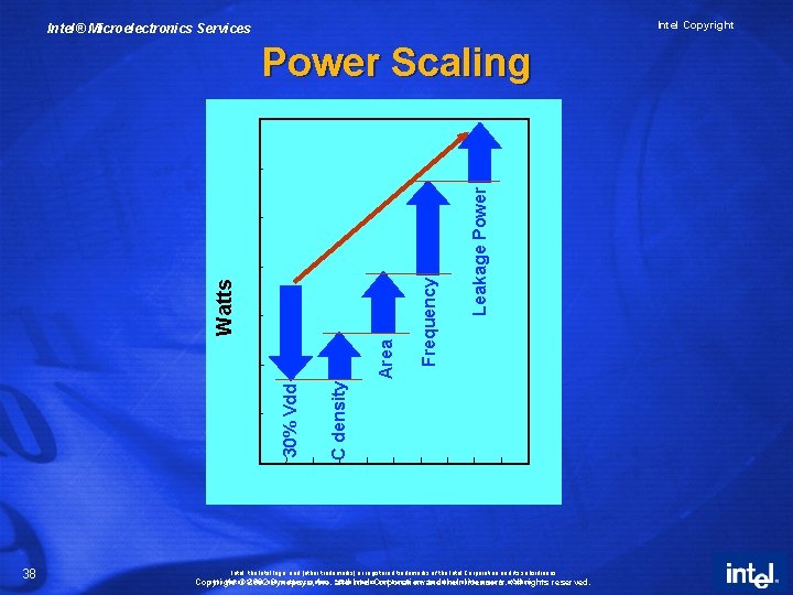
Intel Copyright Intel® Microelectronics Services Power Scaling Power density is increasing 70 Surpassed hot-plate power density in 0. 6 m – Performance (higher freq) – Exponential growth in leakage – Exponential impact on reliability 2 50 Watts/cm Junction Temp <= 100 C is recommended 60 40 30 20 10 0 Intel, the Intel logo, and [other trademarks] or registered trademarks of the Intel Corporation and its subsidiaries in the United in other countries. *Other. Intel names. Corporation and brands may and be claimed the property of. All others. Copyright ©States 2002 and Synopsys, Inc. and theiraslicensors. rights reserved.

Intel Copyright Intel® Microelectronics Services 38 Leakage Power Frequency C density 30% Vdd Area Watts Power Scaling Intel, the Intel logo, and [other trademarks] or registered trademarks of the Intel Corporation and its subsidiaries in the United in other countries. *Other. Intel names. Corporation and brands may and be claimed the property of. All others. Copyright ©States 2002 and Synopsys, Inc. and theiraslicensors. rights reserved.

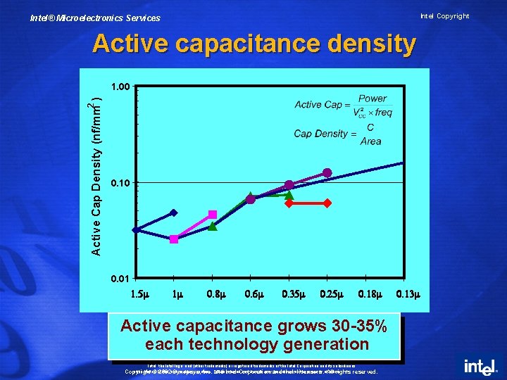
Intel Copyright Intel® Microelectronics Services Active capacitance density 2 Active Cap Density (nf/mm ) 1. 00 0. 10 0. 01 1. 5 m 1 m 0. 8 m 0. 6 m 0. 35 m 0. 25 m 0. 18 m Active capacitance grows 30 -35% each technology generation Intel, the Intel logo, and [other trademarks] or registered trademarks of the Intel Corporation and its subsidiaries in the United in other countries. *Other. Intel names. Corporation and brands may and be claimed the property of. All others. Copyright ©States 2002 and Synopsys, Inc. and theiraslicensors. rights reserved. 0. 13 m

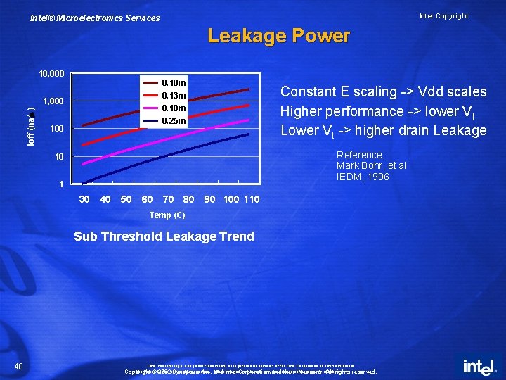
Intel Copyright Intel® Microelectronics Services Leakage Power 10, 000 0. 10 m 0. 13 m 0. 18 m 0. 25 m Ioff (na/ ) 1, 000 100 Constant E scaling -> Vdd scales Higher performance -> lower Vt Lower Vt -> higher drain Leakage Reference: Mark Bohr, et al IEDM, 1996 10 1 30 40 50 60 70 80 90 100 110 Temp (C) Sub Threshold Leakage Trend 40 Intel, the Intel logo, and [other trademarks] or registered trademarks of the Intel Corporation and its subsidiaries in the United in other countries. *Other. Intel names. Corporation and brands may and be claimed the property of. All others. Copyright ©States 2002 and Synopsys, Inc. and theiraslicensors. rights reserved.

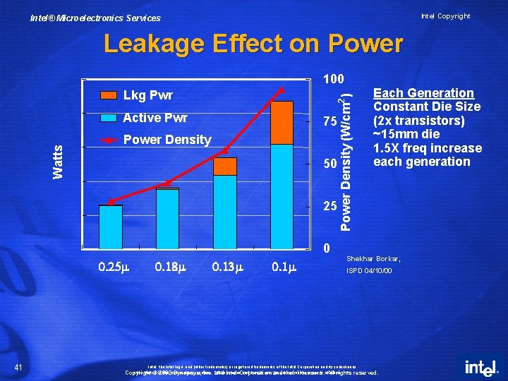
Intel Copyright Intel® Microelectronics Services Leakage Effect on Power 100 Power Density (W/cm 2 ) Lkg Pwr Watts Active Pwr 75 Power Density 50 Each Generation Constant Die Size (2 x transistors) ~15 mm die 1. 5 X freq increase each generation 25 0 0. 25 m 41 0. 18 m 0. 13 m 0. 1 m Shekhar Borkar, ISPD 04/10/00 Intel, the Intel logo, and [other trademarks] or registered trademarks of the Intel Corporation and its subsidiaries in the United in other countries. *Other. Intel names. Corporation and brands may and be claimed the property of. All others. Copyright ©States 2002 and Synopsys, Inc. and theiraslicensors. rights reserved.

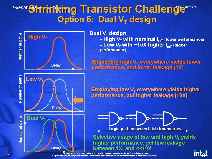
Shrinking Transistor Challenge Intel Copyright Intel® Microelectronics Services Number of paths Option 5: Dual VT design - High VT with nominal Ioff (lower performance) - Low VT with ~10 X higher loff (higher High VT performance) Number of paths Delay Employing high VT everywhere yields lower performance, and lower leakage (1 X) Low VT Employing low VT everywhere yields higher performance, but higher leakage (10 X) Number of paths Delay Dual VT Logic path between latch boundaries Delay 42 Selective usage of low and high Vt yields higher performance, yet low leakage between 1 X, and <<10 X Intel, the Intel logo, and [other trademarks] or registered trademarks of the Intel Corporation and its subsidiaries in the United in other countries. *Other. Intel names. Corporation and brands may and be claimed the property of. All others. Copyright ©States 2002 and Synopsys, Inc. and theiraslicensors. rights reserved.

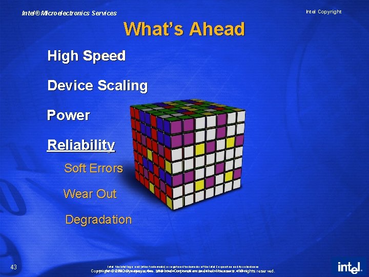
Intel Copyright Intel® Microelectronics Services What’s Ahead High Speed Device Scaling Power Reliability Soft Errors Wear Out Degradation 43 Intel, the Intel logo, and [other trademarks] or registered trademarks of the Intel Corporation and its subsidiaries in the United in other countries. *Other. Intel names. Corporation and brands may and be claimed the property of. All others. Copyright ©States 2002 and Synopsys, Inc. and theiraslicensors. rights reserved.

The Reliability and Quality Challenges § The bathtub curve § Common aging and random failure mechanisms § Hot-e transistor degradation due to hot electrons § EM – electromigration § SH - self heat § Oxide wear out § NBTI – Negative bias temperature instability (P-Channel) § SER - Single-event soft errors 44 Copyright © 2002 Synopsys, Inc. and Intel Corporation and their licensors. All rights reserved.

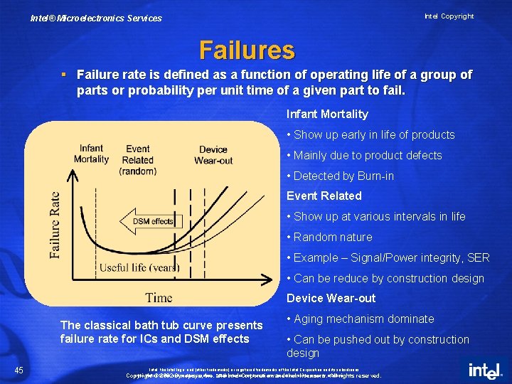
Intel Copyright Intel® Microelectronics Services Failures § Failure rate is defined as a function of operating life of a group of parts or probability per unit time of a given part to fail. Infant Mortality • Show up early in life of products • Mainly due to product defects • Detected by Burn-in Event Related • Show up at various intervals in life • Random nature • Example – Signal/Power integrity, SER • Can be reduce by construction design Device Wear-out The classical bath tub curve presents failure rate for ICs and DSM effects 45 • Aging mechanism dominate • Can be pushed out by construction design Intel, the Intel logo, and [other trademarks] or registered trademarks of the Intel Corporation and its subsidiaries in the United in other countries. *Other. Intel names. Corporation and brands may and be claimed the property of. All others. Copyright ©States 2002 and Synopsys, Inc. and theiraslicensors. rights reserved.

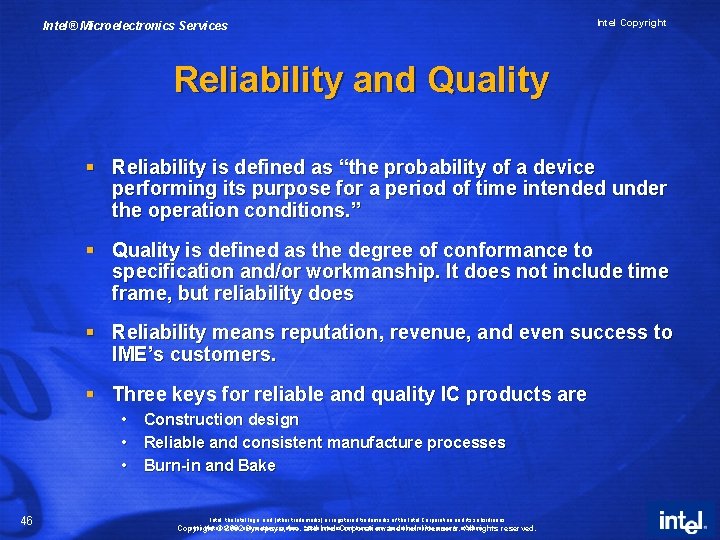
Intel® Microelectronics Services Intel Copyright Reliability and Quality § Reliability is defined as “the probability of a device performing its purpose for a period of time intended under the operation conditions. ” § Quality is defined as the degree of conformance to specification and/or workmanship. It does not include time frame, but reliability does § Reliability means reputation, revenue, and even success to IME’s customers. § Three keys for reliable and quality IC products are • Construction design • Reliable and consistent manufacture processes • Burn-in and Bake 46 Intel, the Intel logo, and [other trademarks] or registered trademarks of the Intel Corporation and its subsidiaries in the United in other countries. *Other. Intel names. Corporation and brands may and be claimed the property of. All others. Copyright ©States 2002 and Synopsys, Inc. and theiraslicensors. rights reserved.

Intel Copyright Intel® Microelectronics Services What’s Ahead High Speed Device Scaling Power Reliability Soft Errors Wear Out Degradation 47 Intel, the Intel logo, and [other trademarks] or registered trademarks of the Intel Corporation and its subsidiaries in the United in other countries. *Other. Intel names. Corporation and brands may and be claimed the property of. All others. Copyright ©States 2002 and Synopsys, Inc. and theiraslicensors. rights reserved.

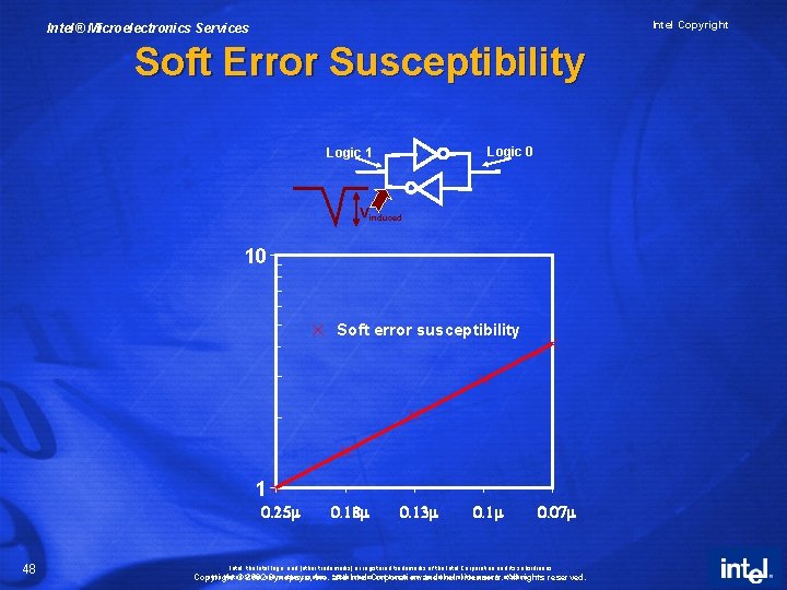
Intel Copyright Intel® Microelectronics Services Soft Error Susceptibility Logic 0 Logic 1 Vinduced 10 Soft error susceptibility 1 0. 25 m 48 0. 18 m 0. 13 m 0. 1 m 0. 07 m Intel, the Intel logo, and [other trademarks] or registered trademarks of the Intel Corporation and its subsidiaries in the United in other countries. *Other. Intel names. Corporation and brands may and be claimed the property of. All others. Copyright ©States 2002 and Synopsys, Inc. and theiraslicensors. rights reserved.

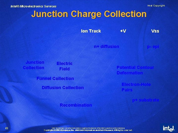
Intel Copyright Intel® Microelectronics Services Junction Charge Collection Ion Track +V Vss n+ diffusion Junction Collection Electric Field p- epi Potential Contour Deformation Funnel Collection Diffusion Collection Electron-Hole Pairs p+ substrate Recombination 49 Intel, the Intel logo, and [other trademarks] or registered trademarks of the Intel Corporation and its subsidiaries in the United in other countries. *Other. Intel names. Corporation and brands may and be claimed the property of. All others. Copyright ©States 2002 and Synopsys, Inc. and theiraslicensors. rights reserved.

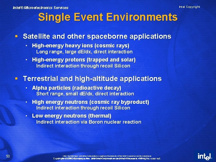
Intel® Microelectronics Services Single Event Environments § Satellite and other spaceborne applications • High-energy heavy ions (cosmic rays) Long range, large d. E/dx, direct interaction • High-energy protons (trapped and solar) Indirect interaction through recoil Silicon § Terrestrial and high-altitude applications • Alpha particles (radioactive decay) Short range, small d. E/dx, direct interaction • High energy neutrons (cosmic ray byproduct) Indirect interaction through recoil Silicon • Low energy neutrons (thermal) Indirect interaction via Boron nuclear reaction 50 Intel, the Intel logo, and [other trademarks] or registered trademarks of the Intel Corporation and its subsidiaries in the United in other countries. *Other. Intel names. Corporation and brands may and be claimed the property of. All others. Copyright ©States 2002 and Synopsys, Inc. and theiraslicensors. rights reserved. Intel Copyright

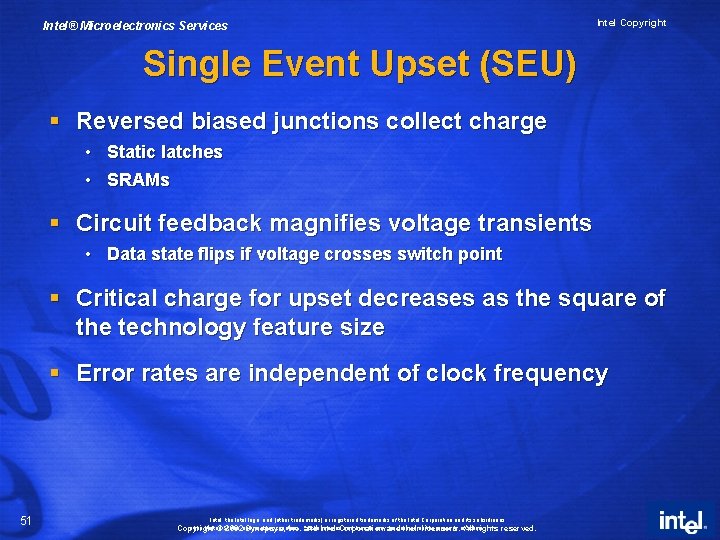
Intel® Microelectronics Services Intel Copyright Single Event Upset (SEU) § Reversed biased junctions collect charge • Static latches • SRAMs § Circuit feedback magnifies voltage transients • Data state flips if voltage crosses switch point § Critical charge for upset decreases as the square of the technology feature size § Error rates are independent of clock frequency 51 Intel, the Intel logo, and [other trademarks] or registered trademarks of the Intel Corporation and its subsidiaries in the United in other countries. *Other. Intel names. Corporation and brands may and be claimed the property of. All others. Copyright ©States 2002 and Synopsys, Inc. and theiraslicensors. rights reserved.

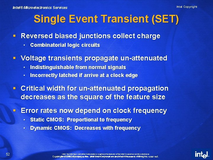
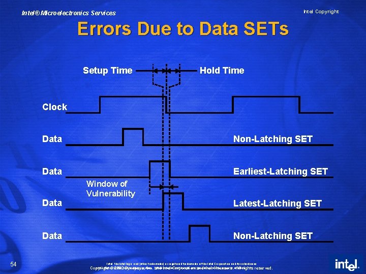
Intel® Microelectronics Services Intel Copyright Single Event Transient (SET) § Reversed biased junctions collect charge • Combinatorial logic circuits § Voltage transients propagate un-attenuated • Indistinguishable from normal signals • Incorrectly latched if arrive at a clock edge § Critical width for un-attenuated propagation decreases as the square of the feature size § Error rates now depend on clock frequency • Static CMOS: Proportional to frequency • Dynamic CMOS: Decreases with frequency 52 Intel, the Intel logo, and [other trademarks] or registered trademarks of the Intel Corporation and its subsidiaries in the United in other countries. *Other. Intel names. Corporation and brands may and be claimed the property of. All others. Copyright ©States 2002 and Synopsys, Inc. and theiraslicensors. rights reserved.

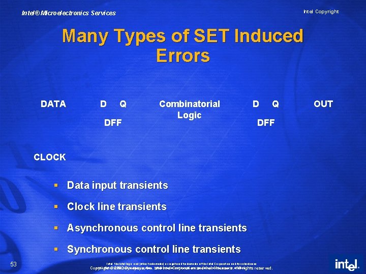
Intel Copyright Intel® Microelectronics Services Many Types of SET Induced Errors DATA D Q DFF Combinatorial Logic D Q DFF CLOCK § Data input transients § Clock line transients § Asynchronous control line transients § Synchronous control line transients 53 Intel, the Intel logo, and [other trademarks] or registered trademarks of the Intel Corporation and its subsidiaries in the United in other countries. *Other. Intel names. Corporation and brands may and be claimed the property of. All others. Copyright ©States 2002 and Synopsys, Inc. and theiraslicensors. rights reserved. OUT

Intel Copyright Intel® Microelectronics Services Errors Due to Data SETs Setup Time Hold Time Clock Data Non-Latching SET Data Earliest-Latching SET Data 54 Window of Vulnerability Latest-Latching SET Non-Latching SET Intel, the Intel logo, and [other trademarks] or registered trademarks of the Intel Corporation and its subsidiaries in the United in other countries. *Other. Intel names. Corporation and brands may and be claimed the property of. All others. Copyright ©States 2002 and Synopsys, Inc. and theiraslicensors. rights reserved.

Intel Copyright Intel® Microelectronics Services What’s Ahead High Speed Device Scaling Power Reliability Soft Errors Wear Out Degradation 55 Intel, the Intel logo, and [other trademarks] or registered trademarks of the Intel Corporation and its subsidiaries in the United in other countries. *Other. Intel names. Corporation and brands may and be claimed the property of. All others. Copyright ©States 2002 and Synopsys, Inc. and theiraslicensors. rights reserved.

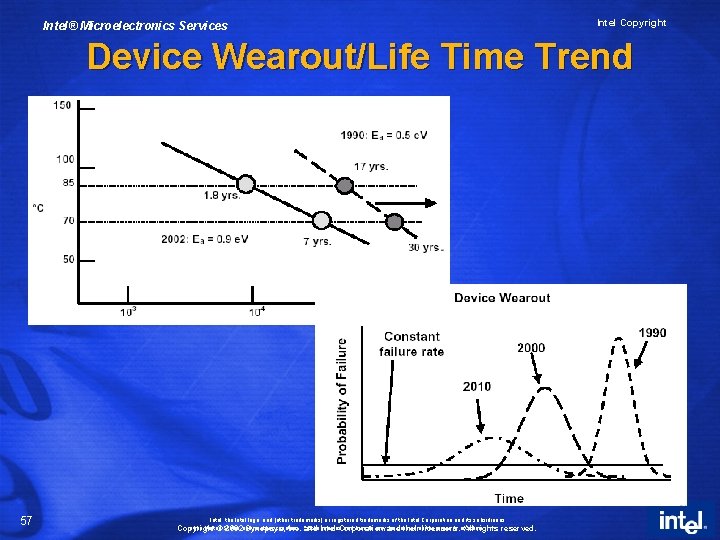
Intel® Microelectronics Services Intel Copyright Oxide Wear-Out § Oxide wearout is a time and voltage dependent oxide breakdown • Very little changes in transistor characteristics before failure • Failure evolves from recoverable soft breakdown to nonrecoverable hard breakdown 56 Intel, the Intel logo, and [other trademarks] or registered trademarks of the Intel Corporation and its subsidiaries in the United in other countries. *Other. Intel names. Corporation and brands may and be claimed the property of. All others. Copyright ©States 2002 and Synopsys, Inc. and theiraslicensors. rights reserved.

Intel® Microelectronics Services Intel Copyright Device Wearout/Life Time Trend 57 Intel, the Intel logo, and [other trademarks] or registered trademarks of the Intel Corporation and its subsidiaries in the United in other countries. *Other. Intel names. Corporation and brands may and be claimed the property of. All others. Copyright ©States 2002 and Synopsys, Inc. and theiraslicensors. rights reserved.

Intel Copyright Intel® Microelectronics Services What’s Ahead High Speed Device Scaling Power Reliability Soft Errors Wear Out Degradation 58 Intel, the Intel logo, and [other trademarks] or registered trademarks of the Intel Corporation and its subsidiaries in the United in other countries. *Other. Intel names. Corporation and brands may and be claimed the property of. All others. Copyright ©States 2002 and Synopsys, Inc. and theiraslicensors. rights reserved.

Intel® Microelectronics Services Common Aging Failure Mechanisms § Hot Electron Degradation § Negative Bias Temperature instability § Oxide wear-out § Electromigration § Self-Heat 59 Intel, the Intel logo, and [other trademarks] or registered trademarks of the Intel Corporation and its subsidiaries in the United in other countries. *Other. Intel names. Corporation and brands may and be claimed the property of. All others. Copyright ©States 2002 and Synopsys, Inc. and theiraslicensors. rights reserved. Intel Copyright
![Intel Microelectronics Services HotE Degradation 60 Intel the Intel logo and other trademarks or Intel® Microelectronics Services Hot-E Degradation 60 Intel, the Intel logo, and [other trademarks] or](https://slidetodoc.com/presentation_image/4e1f36ad53a92152eff69dd703246d07/image-59.jpg)
Intel® Microelectronics Services Hot-E Degradation 60 Intel, the Intel logo, and [other trademarks] or registered trademarks of the Intel Corporation and its subsidiaries in the United in other countries. *Other. Intel names. Corporation and brands may and be claimed the property of. All others. Copyright ©States 2002 and Synopsys, Inc. and theiraslicensors. rights reserved. Intel Copyright

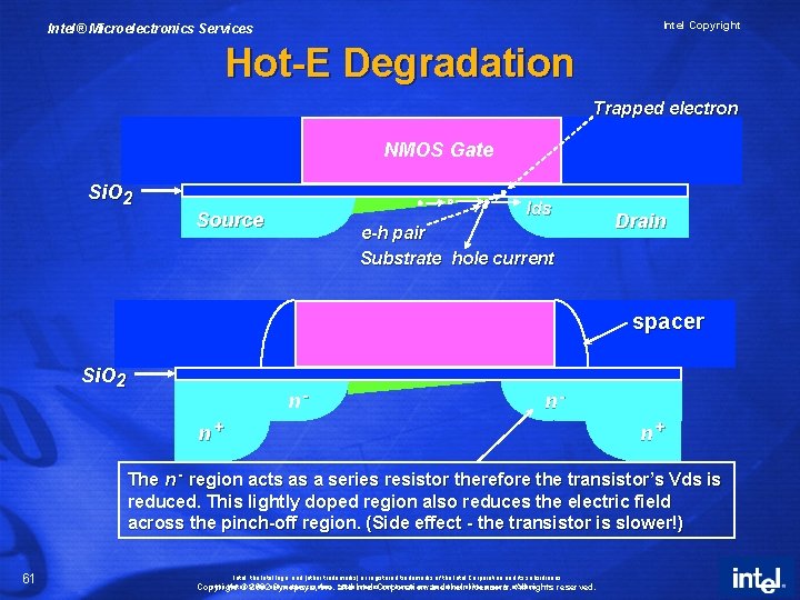
Intel Copyright Intel® Microelectronics Services Hot-E Degradation Trapped electron NMOS Gate Si. O 2 Ids Source e-h pair Substrate hole current Drain spacer Si. O 2 n- n- n+ n+ The n - region acts as a series resistor therefore the transistor’s Vds is reduced. This lightly doped region also reduces the electric field across the pinch-off region. (Side effect - the transistor is slower!) 61 Intel, the Intel logo, and [other trademarks] or registered trademarks of the Intel Corporation and its subsidiaries in the United in other countries. *Other. Intel names. Corporation and brands may and be claimed the property of. All others. Copyright ©States 2002 and Synopsys, Inc. and theiraslicensors. rights reserved.

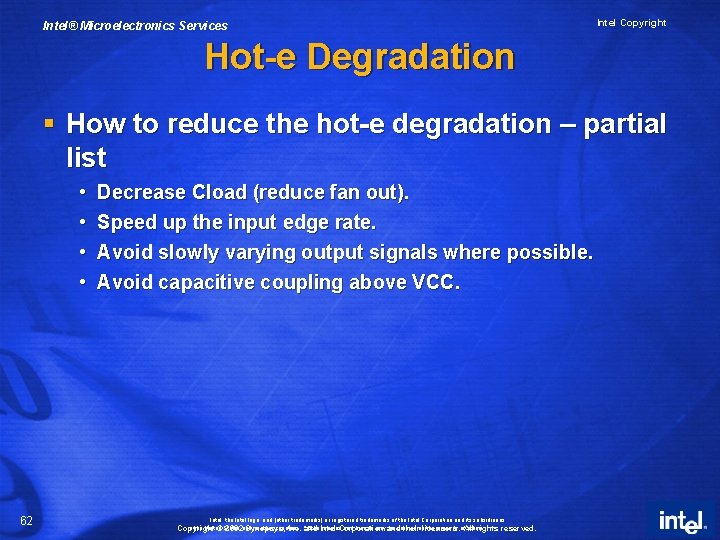
Intel® Microelectronics Services Intel Copyright Hot-e Degradation § How to reduce the hot-e degradation – partial list • • 62 Decrease Cload (reduce fan out). Speed up the input edge rate. Avoid slowly varying output signals where possible. Avoid capacitive coupling above VCC. Intel, the Intel logo, and [other trademarks] or registered trademarks of the Intel Corporation and its subsidiaries in the United in other countries. *Other. Intel names. Corporation and brands may and be claimed the property of. All others. Copyright ©States 2002 and Synopsys, Inc. and theiraslicensors. rights reserved.

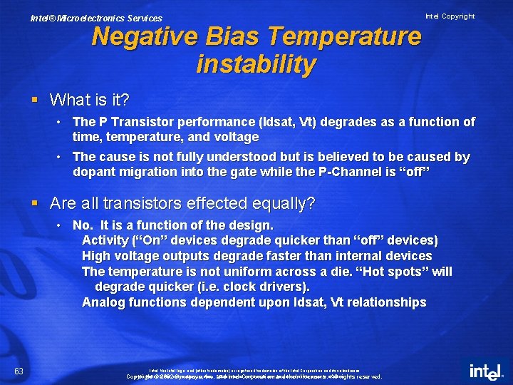
Intel® Microelectronics Services Intel Copyright Negative Bias Temperature instability § What is it? • The P Transistor performance (Idsat, Vt) degrades as a function of time, temperature, and voltage • The cause is not fully understood but is believed to be caused by dopant migration into the gate while the P-Channel is “off” § Are all transistors effected equally? • No. It is a function of the design. Activity (“On” devices degrade quicker than “off” devices) High voltage outputs degrade faster than internal devices The temperature is not uniform across a die. “Hot spots” will degrade quicker (i. e. clock drivers). Analog functions dependent upon Idsat, Vt relationships 63 Intel, the Intel logo, and [other trademarks] or registered trademarks of the Intel Corporation and its subsidiaries in the United in other countries. *Other. Intel names. Corporation and brands may and be claimed the property of. All others. Copyright ©States 2002 and Synopsys, Inc. and theiraslicensors. rights reserved.

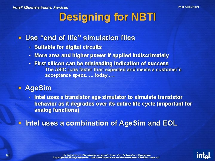
Intel® Microelectronics Services Intel Copyright Designing for NBTI § Use “end of life” simulation files • • • Suitable for digital circuits More area and higher power if applied indiscrimately First silicon can be misleading indication of success The ASIC runs faster than expected and meets a customer’s acceptance specs…. . today…. . § Age. Sim • Intel uses a transistor age simulator to simulate transistor behavior as it degrades over its entire life cycle (important for analog functions) § Intel uses a combination of Age. Sim and EOL 64 Intel, the Intel logo, and [other trademarks] or registered trademarks of the Intel Corporation and its subsidiaries in the United in other countries. *Other. Intel names. Corporation and brands may and be claimed the property of. All others. Copyright ©States 2002 and Synopsys, Inc. and theiraslicensors. rights reserved.

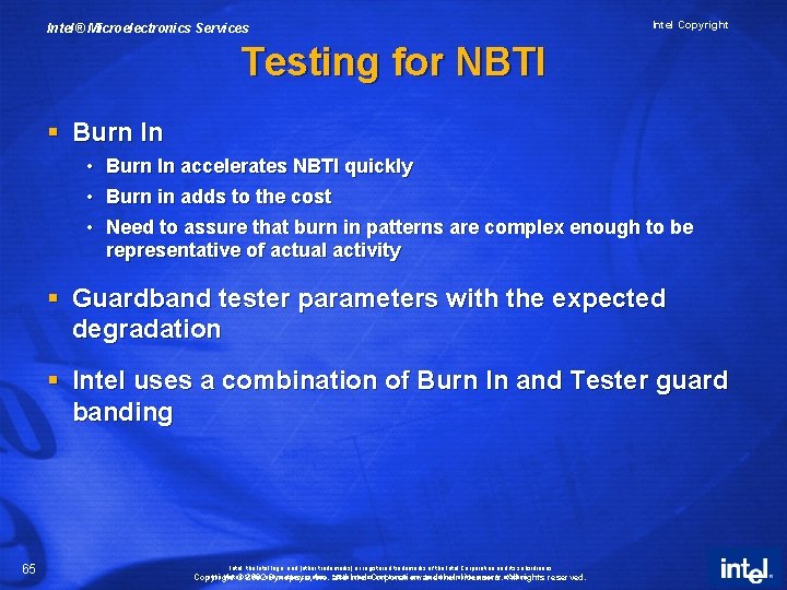
Intel® Microelectronics Services Intel Copyright Testing for NBTI § Burn In • Burn In accelerates NBTI quickly • Burn in adds to the cost • Need to assure that burn in patterns are complex enough to be representative of actual activity § Guardband tester parameters with the expected degradation § Intel uses a combination of Burn In and Tester guard banding 65 Intel, the Intel logo, and [other trademarks] or registered trademarks of the Intel Corporation and its subsidiaries in the United in other countries. *Other. Intel names. Corporation and brands may and be claimed the property of. All others. Copyright ©States 2002 and Synopsys, Inc. and theiraslicensors. rights reserved.

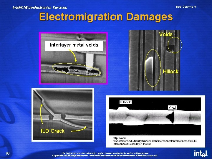
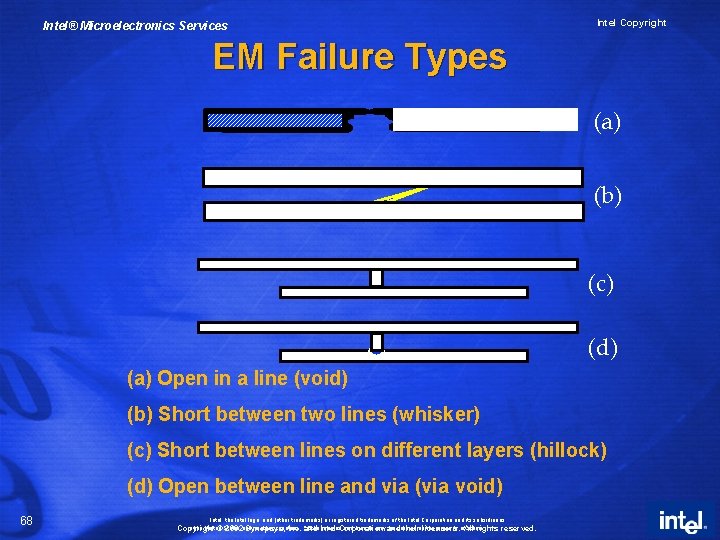
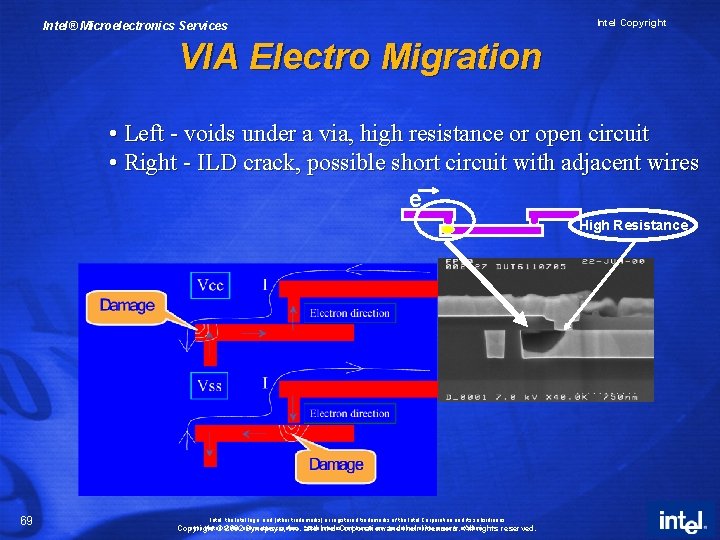
Intel Copyright Intel® Microelectronics Services Electromigration Damages Voids Interlayer metal voids Hillock ILD Crack 66 Intel, the Intel logo, and [other trademarks] or registered trademarks of the Intel Corporation and its subsidiaries in the United in other countries. *Other. Intel names. Corporation and brands may and be claimed the property of. All others. Copyright ©States 2002 and Synopsys, Inc. and theiraslicensors. rights reserved.

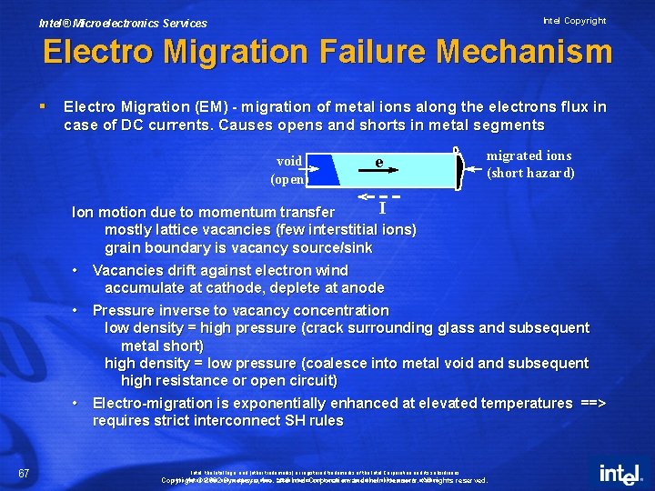
Intel Copyright Intel® Microelectronics Services Electro Migration Failure Mechanism § Electro Migration (EM) - migration of metal ions along the electrons flux in case of DC currents. Causes opens and shorts in metal segments void (open) e migrated ions (short hazard) I Ion motion due to momentum transfer mostly lattice vacancies (few interstitial ions) grain boundary is vacancy source/sink • Vacancies drift against electron wind accumulate at cathode, deplete at anode • Pressure inverse to vacancy concentration low density = high pressure (crack surrounding glass and subsequent metal short) high density = low pressure (coalesce into metal void and subsequent high resistance or open circuit) • Electro-migration is exponentially enhanced at elevated temperatures ==> requires strict interconnect SH rules 67 Intel, the Intel logo, and [other trademarks] or registered trademarks of the Intel Corporation and its subsidiaries in the United in other countries. *Other. Intel names. Corporation and brands may and be claimed the property of. All others. Copyright ©States 2002 and Synopsys, Inc. and theiraslicensors. rights reserved.

Intel® Microelectronics Services Intel Copyright EM Failure Types (a) (b) (c) (d) (a) Open in a line (void) (b) Short between two lines (whisker) (c) Short between lines on different layers (hillock) (d) Open between line and via (via void) 68 Intel, the Intel logo, and [other trademarks] or registered trademarks of the Intel Corporation and its subsidiaries in the United in other countries. *Other. Intel names. Corporation and brands may and be claimed the property of. All others. Copyright ©States 2002 and Synopsys, Inc. and theiraslicensors. rights reserved.

Intel® Microelectronics Services Intel Copyright VIA Electro Migration • Left - voids under a via, high resistance or open circuit • Right - ILD crack, possible short circuit with adjacent wires e High Resistance 69 Intel, the Intel logo, and [other trademarks] or registered trademarks of the Intel Corporation and its subsidiaries in the United in other countries. *Other. Intel names. Corporation and brands may and be claimed the property of. All others. Copyright ©States 2002 and Synopsys, Inc. and theiraslicensors. rights reserved.

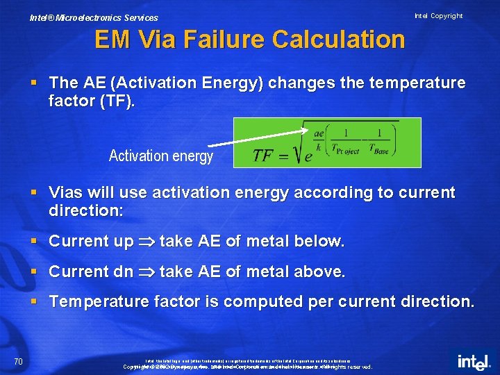
Intel® Microelectronics Services Intel Copyright EM Via Failure Calculation § The AE (Activation Energy) changes the temperature factor (TF). Activation energy § Vias will use activation energy according to current direction: § Current up take AE of metal below. § Current dn take AE of metal above. § Temperature factor is computed per current direction. 70 Intel, the Intel logo, and [other trademarks] or registered trademarks of the Intel Corporation and its subsidiaries in the United in other countries. *Other. Intel names. Corporation and brands may and be claimed the property of. All others. Copyright ©States 2002 and Synopsys, Inc. and theiraslicensors. rights reserved.

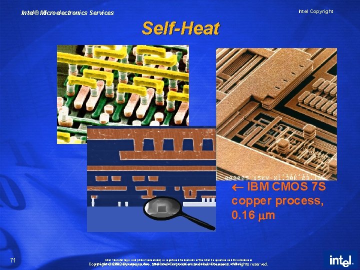
Intel Copyright Intel® Microelectronics Services Self-Heat IBM CMOS 7 S copper process, 0. 16 mm 71 Intel, the Intel logo, and [other trademarks] or registered trademarks of the Intel Corporation and its subsidiaries in the United in other countries. *Other. Intel names. Corporation and brands may and be claimed the property of. All others. Copyright ©States 2002 and Synopsys, Inc. and theiraslicensors. rights reserved.

Intel Copyright Intel® Microelectronics Services Self Heat (SH) § SH is the rise in temperature due to the electron movement within a conductor. § It is also known as Joule Heating, since it is related to the power that is dissipated onto the interconnect. § SH is dependant on bi-directional AC (Root Mean Squared) current, since Joule heating is a result of P=I 2 R. § SH also has a Design Rule Current Density JMAX for each layer. A SH violation occurs when J > JMAX. 72 Intel, the Intel logo, and [other trademarks] or registered trademarks of the Intel Corporation and its subsidiaries in the United in other countries. *Other. Intel names. Corporation and brands may and be claimed the property of. All others. Copyright ©States 2002 and Synopsys, Inc. and theiraslicensors. rights reserved.

Intel® Microelectronics Services Intel Copyright Self Heating = More EM § Self Heating ? More EM. D Since SH increases temperature, self-heating on a metal line can aggravate EM effects. D SH on a line can also increase EM effects on neighboring lines. § Because self-heating contributes to electromigration, failures are typically labeled as EM, not SH. 73 Intel, the Intel logo, and [other trademarks] or registered trademarks of the Intel Corporation and its subsidiaries in the United in other countries. *Other. Intel names. Corporation and brands may and be claimed the property of. All others. Copyright ©States 2002 and Synopsys, Inc. and theiraslicensors. rights reserved.