Unit III Nonlinear Applications of OPAMP 8 Hrs
- Slides: 35

Unit III : Non-linear Applications of OP-AMP (8 Hrs) § Comparator, characteristics of comparator, applications of comparator, § Schmitt trigger (symmetrical/asymmetrical), clippers and clampers, voltage limiters, § Square wave generator, triangular wave generator, § Need of precision rectifier, Half wave , Full wave precision rectifiers, § peak detectors, sample and hold circuits

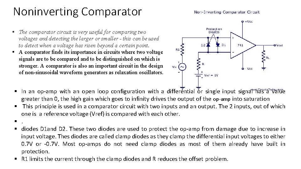
Noninverting Comparator § The comparator circuit is very useful for comparing two voltages and detecting the larger or smaller - this can be used to detect when a voltage has risen beyond a certain point. § A comparator finds its importance in circuits where two voltage signals are to be compared and to be distinguished on which is stronger. A comparator is also an important circuit in the design of non-sinusoidal waveform generators as relaxation oscillators. § In an op-amp with an open loop configuration with a differential or single input signal has a value greater than 0, the high gain which goes to infinity drives the output of the op-amp into saturation § This principle is used in a comparator circuit with two inputs and an output. The 2 inputs, out of which one is a reference voltage (Vref) is compared with each other. §. § diodes D 1 and D 2. These two diodes are used to protect the op-amp from damage due to increase in input voltage. Thes diodes are called clamp diodes as they clamp the differential input voltages to either 0. 7 V or -0. 7 V. Most op-amps do not need clamp diodes as most of them already have built in protection. § R 1 limits the current through the clamp diodes and R reduces the offset problem.

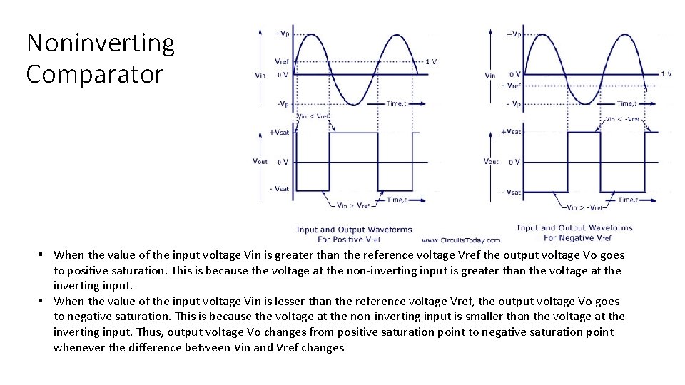
Noninverting Comparator § When the value of the input voltage Vin is greater than the reference voltage Vref the output voltage Vo goes to positive saturation. This is because the voltage at the non-inverting input is greater than the voltage at the inverting input. § When the value of the input voltage Vin is lesser than the reference voltage Vref, the output voltage Vo goes to negative saturation. This is because the voltage at the non-inverting input is smaller than the voltage at the inverting input. Thus, output voltage Vo changes from positive saturation point to negative saturation point whenever the difference between Vin and Vref changes

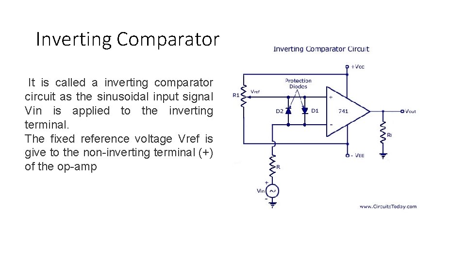
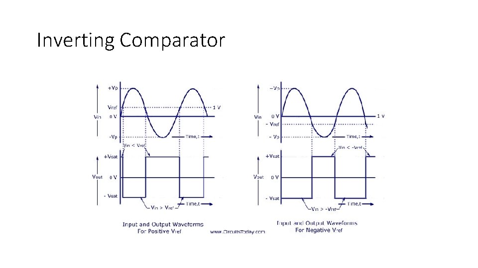
Inverting Comparator It is called a inverting comparator circuit as the sinusoidal input signal Vin is applied to the inverting terminal. The fixed reference voltage Vref is give to the non-inverting terminal (+) of the op-amp

Inverting Comparator

Comparator Characteristics • Operation Speed – According to change of conditions in the input, a comparator circuit switches at a good speed beween the saturation levels and the response is instantaneous. • Accuracy – Accuracy of the comparator circuit causes the following characteristics: • High Voltage Gain – The comparator circuit is said to have a high voltage gain characteristic that results in the requirement of smaller hysteresis voltage. As a result the comparator output voltage switches between the upper and lower saturation levels. • High Common Mode Rejection Ratio (CMRR) – The common mode input voltage parameters such a noise is rejected with the help of a high CMRR. • Very Small Input Offset Current and Input Offset Voltage – A negligible amount of Input Offset Current and Input Offset Voltage causes a lesser amount of offset problems. To reduce further offset problems, offset voltage compensating networks and offset minimizing resistors can be used.

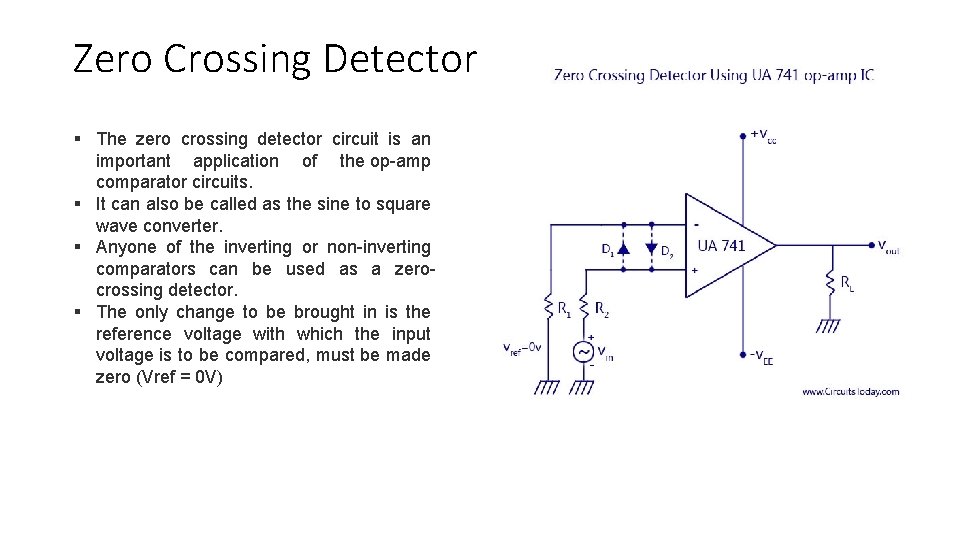
Zero Crossing Detector § The zero crossing detector circuit is an important application of the op-amp comparator circuits. § It can also be called as the sine to square wave converter. § Anyone of the inverting or non-inverting comparators can be used as a zerocrossing detector. § The only change to be brought in is the reference voltage with which the input voltage is to be compared, must be made zero (Vref = 0 V)

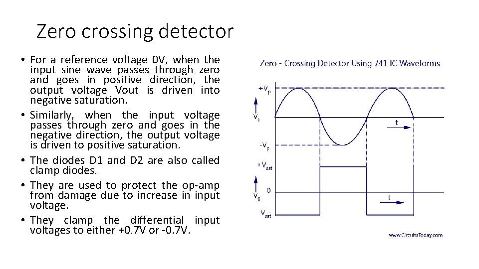
Zero crossing detector • For a reference voltage 0 V, when the input sine wave passes through zero and goes in positive direction, the output voltage Vout is driven into negative saturation. • Similarly, when the input voltage passes through zero and goes in the negative direction, the output voltage is driven to positive saturation. • The diodes D 1 and D 2 are also called clamp diodes. • They are used to protect the op-amp from damage due to increase in input voltage. • They clamp the differential input voltages to either +0. 7 V or -0. 7 V.

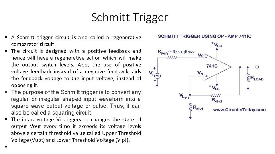
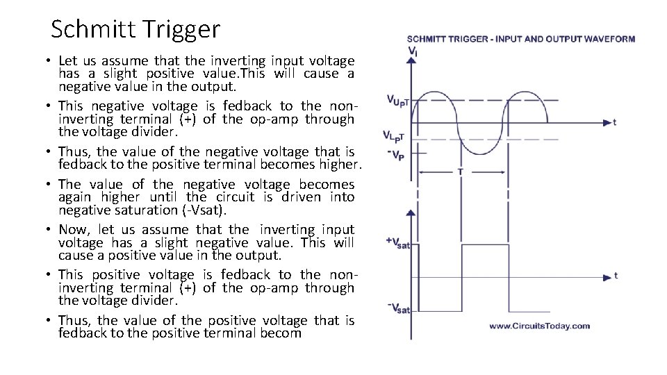
Schmitt Trigger § A Schmitt trigger circuit is also called a regenerative comparator circuit. § The circuit is designed with a positive feedback and hence will have a regenerative action which will make the output switch levels. Also, the use of positive voltage feedback instead of a negative feedback, aids the feedback voltage to the input voltage, instead of opposing it. § The purpose of the Schmitt trigger is to convert any regular or irregular shaped input waveform into a square wave output voltage or pulse. Thus, it can also be called a squaring circuit. § The input voltage Vi triggers or changes the state of output Vout every time it exceeds its voltage levels above a certain threshold value called Upper Threshold Voltage (Vupt) and Lower Threshold Voltage (Vlpt). §

Schmitt Trigger • Let us assume that the inverting input voltage has a slight positive value. This will cause a negative value in the output. • This negative voltage is fedback to the noninverting terminal (+) of the op-amp through the voltage divider. • Thus, the value of the negative voltage that is fedback to the positive terminal becomes higher. • The value of the negative voltage becomes again higher until the circuit is driven into negative saturation (-Vsat). • Now, let us assume that the inverting input voltage has a slight negative value. This will cause a positive value in the output. • This positive voltage is fedback to the noninverting terminal (+) of the op-amp through the voltage divider. • Thus, the value of the positive voltage that is fedback to the positive terminal becom

Schmitt Trigger • When Vout = +Vsat, the voltage across Rdiv 1 is called Upper Threshold Voltage (Vupt). • The input voltage, Vin must be slightly more positive than Vupt inorder to cause the output Vo to switch from +Vsat to -Vsat. • When the input voltage is less than Vupt, the output voltage Vout is at +Vsat. • Upper Threshold Voltage, Vupt = +Vsat (Rdiv 1/[Rdiv 1+Rdiv 2]) • When Vout = -Vsat, the voltage across Rdiv 1 is called Lower Threshold Voltage (Vlpt). • The input voltage, Vin must be slightly more negaitive than Vlpt inorder to cause the output Vo to switch from Vsat to +Vsat. • When the input voltage is less than Vlpt, the output voltage Vout is at -Vsat. • Lower Threshold Voltage, Vlpt = -Vsat (Rdiv 1/[Rdiv 1+Rdiv 2]) • If the value of Vupt and Vlpt are higher than the input noise voltage, the positive feedback will eliminate the false output transitions. • With the help of positive feedback and its regenerative behavior, the output voltage will switch fast between the positive and negative saturation voltages.

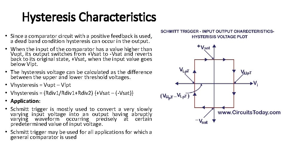
Hysteresis Characteristics • Since a comparator circuit with a positive feedback is used, a dead band condition hysteresis can occur in the output. • When the input of the comparator has a value higher than Vupt, its output switches from +Vsat to -Vsat and reverts back to its original state, +Vsat, when the input value goes below Vlpt. • The hysteresis voltage can be calculated as the difference between the upper and lower threshold voltages. • Vhysteresis = Vupt – Vlpt • Vhysteresis = (Rdiv 1/Rdiv 1+Rdiv 2) {+Vsat – (-Vsat)} • Application: • Schmitt trigger is mostly used to convert a very slowly varying input voltage into an output having abruptly varying waveform occurring precisely at certain predetermined value of input voltage. • Schmitt trigger may be used for all applications for which a general comparator is used

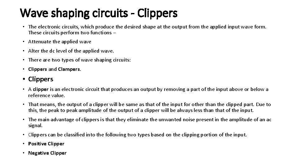
Wave shaping circuits - Clippers • The electronic circuits, which produce the desired shape at the output from the applied input wave form. These circuits perform two functions − • Attenuate the applied wave • Alter the dc level of the applied wave. • There are two types of wave shaping circuits: • Clippers and Clampers. • Clippers • A clipper is an electronic circuit that produces an output by removing a part of the input above or below a reference value. • That means, the output of a clipper will be same as that of the input for other than the clipped part. Due to this, the peak to peak amplitude of the output of a clipper will be always less than that of the input. • The main advantage of clippers is that they eliminate the unwanted noise present in the amplitude of an ac signal. • Clippers can be classified into the following two types based on the clipping portion of the input. • Positive Clipper • Negative Clipper

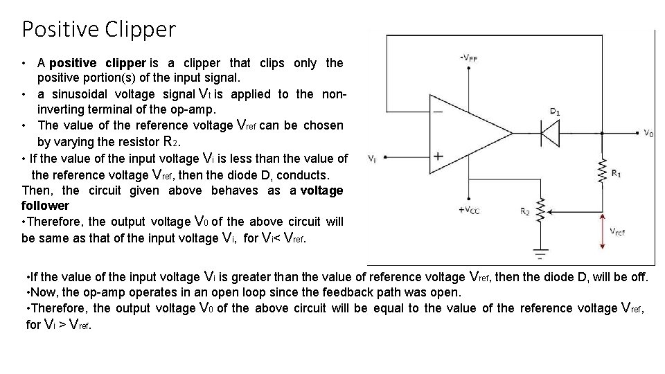
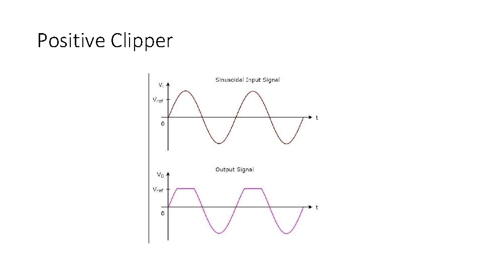
Positive Clipper • A positive clipper is a clipper that clips only the positive portion(s) of the input signal. • a sinusoidal voltage signal Vt is applied to the noninverting terminal of the op-amp. • The value of the reference voltage Vref can be chosen by varying the resistor R 2. • If the value of the input voltage Vi is less than the value of the reference voltage Vref, then the diode D conducts. Then, the circuit given above behaves as a voltage follower • Therefore, the output voltage V 0 of the above circuit will be same as that of the input voltage Vi, for Vi< Vref. 1 • If the value of the input voltage Vi is greater than the value of reference voltage Vref, then the diode D will be off. • Now, the op-amp operates in an open loop since the feedback path was open. • Therefore, the output voltage V 0 of the above circuit will be equal to the value of the reference voltage Vref, for Vi > Vref. 1

Positive Clipper

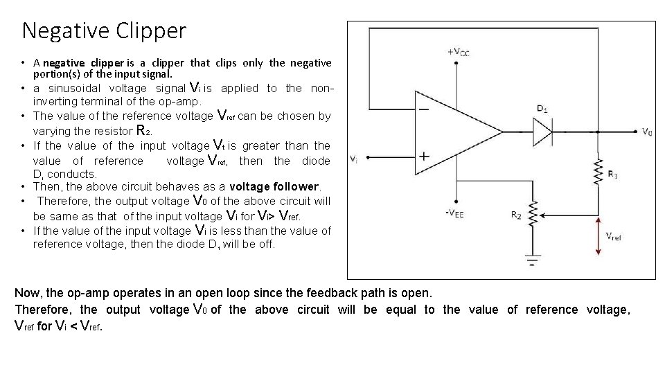
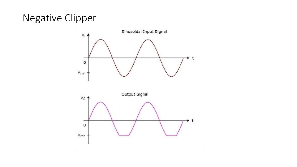
Negative Clipper • A negative clipper is a clipper that clips only the negative portion(s) of the input signal. • a sinusoidal voltage signal Vi is applied to the noninverting terminal of the op-amp. • The value of the reference voltage Vref can be chosen by varying the resistor R 2. • If the value of the input voltage Vt is greater than the value of reference voltage Vref, then the diode D conducts. • Then, the above circuit behaves as a voltage follower. • Therefore, the output voltage V 0 of the above circuit will be same as that of the input voltage Vi for Vi> Vref. • If the value of the input voltage Vi is less than the value of reference voltage, then the diode D will be off. 1 1 Now, the op-amp operates in an open loop since the feedback path is open. Therefore, the output voltage V 0 of the above circuit will be equal to the value of reference voltage, Vref for Vi < Vref.

Negative Clipper

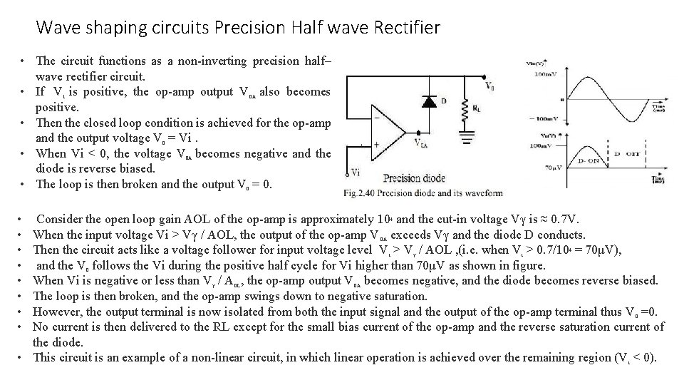
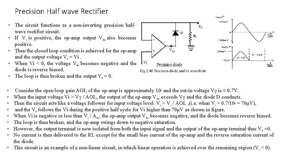
Wave shaping circuits Precision Half wave Rectifier • The circuit functions as a non-inverting precision half– wave rectifier circuit. • If V is positive, the op-amp output V also becomes positive. • Then the closed loop condition is achieved for the op-amp and the output voltage V = Vi. • When Vi < 0, the voltage V becomes negative and the diode is reverse biased. • The loop is then broken and the output V = 0. 1 OA 0 0 A 0 • • Consider the open loop gain AOL of the op-amp is approximately 104 and the cut-in voltage Vγ is ≈ 0. 7 V. When the input voltage Vi > Vγ / AOL, the output of the op-amp VOA exceeds Vγ and the diode D conducts. Then the circuit acts like a voltage follower for input voltage level Vi > Vγ / AOL , (i. e. when Vi > 0. 7/104 = 70μV), and the V 0 follows the Vi during the positive half cycle for Vi higher than 70μV as shown in figure. When Vi is negative or less than Vγ / AOL, the op-amp output VOA becomes negative, and the diode becomes reverse biased. The loop is then broken, and the op-amp swings down to negative saturation. However, the output terminal is now isolated from both the input signal and the output of the op-amp terminal thus V 0 =0. No current is then delivered to the RL except for the small bias current of the op-amp and the reverse saturation current of the diode. • This circuit is an example of a non-linear circuit, in which linear operation is achieved over the remaining region (V i < 0).

Wave shaping circuits Clampers • The output of a clamper is an exact replica of the input. Hence, the peak to peak amplitude of the output of a clamper will be always equal to that of the input. • Clampers are used to introduce or restore the DC level of input signal at the output. • There are two types of op-amp based clampers based on the DC shift of the input. • Positive Clamper • Negative Clamper

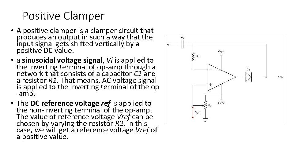
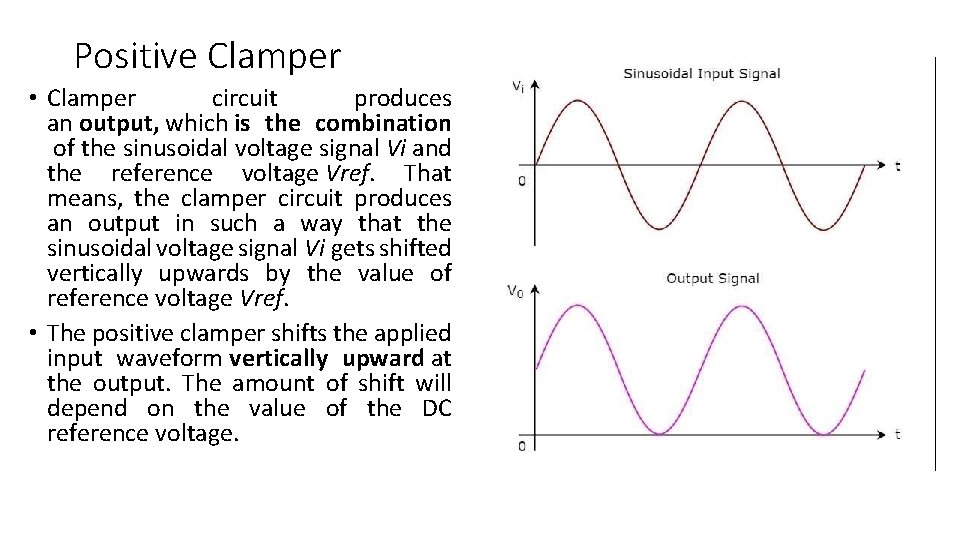
Positive Clamper • A positive clamper is a clamper circuit that produces an output in such a way that the input signal gets shifted vertically by a positive DC value. • a sinusoidal voltage signal, Vi is applied to the inverting terminal of op-amp through a network that consists of a capacitor C 1 and a resistor R 1. That means, AC voltage signal is applied to the inverting terminal of the op -amp. • The DC reference voltage ref is applied to the non-inverting terminal of the op-amp. The value of reference voltage Vref can be chosen by varying the resistor R 2. In this case, we will get a reference voltage Vref of a positive value.

Positive Clamper • Clamper circuit produces an output, which is the combination of the sinusoidal voltage signal Vi and the reference voltage Vref. That means, the clamper circuit produces an output in such a way that the sinusoidal voltage signal Vi gets shifted vertically upwards by the value of reference voltage Vref. • The positive clamper shifts the applied input waveform vertically upward at the output. The amount of shift will depend on the value of the DC reference voltage.

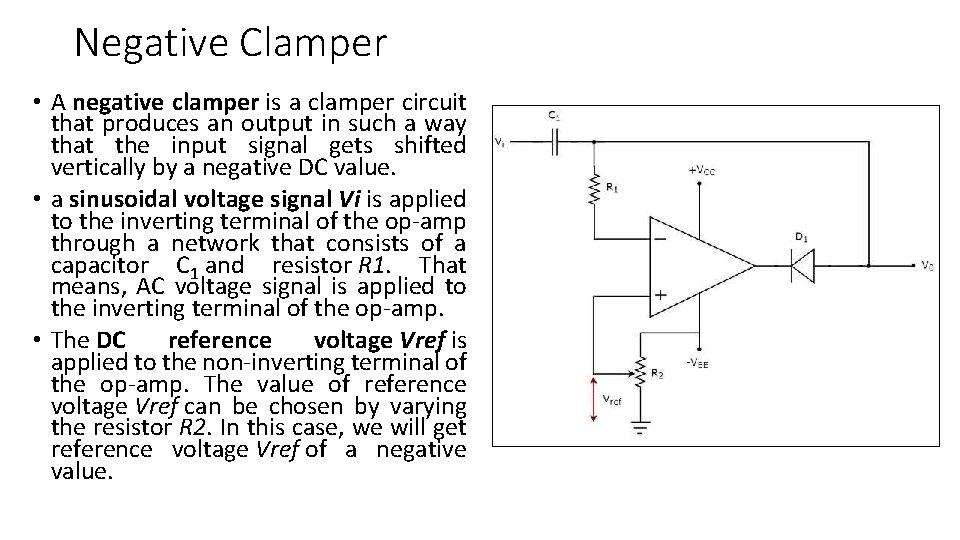
Negative Clamper • A negative clamper is a clamper circuit that produces an output in such a way that the input signal gets shifted vertically by a negative DC value. • a sinusoidal voltage signal Vi is applied to the inverting terminal of the op-amp through a network that consists of a capacitor C 1 and resistor R 1. That means, AC voltage signal is applied to the inverting terminal of the op-amp. • The DC reference voltage Vref is applied to the non-inverting terminal of the op-amp. The value of reference voltage Vref can be chosen by varying the resistor R 2. In this case, we will get reference voltage Vref of a negative value.

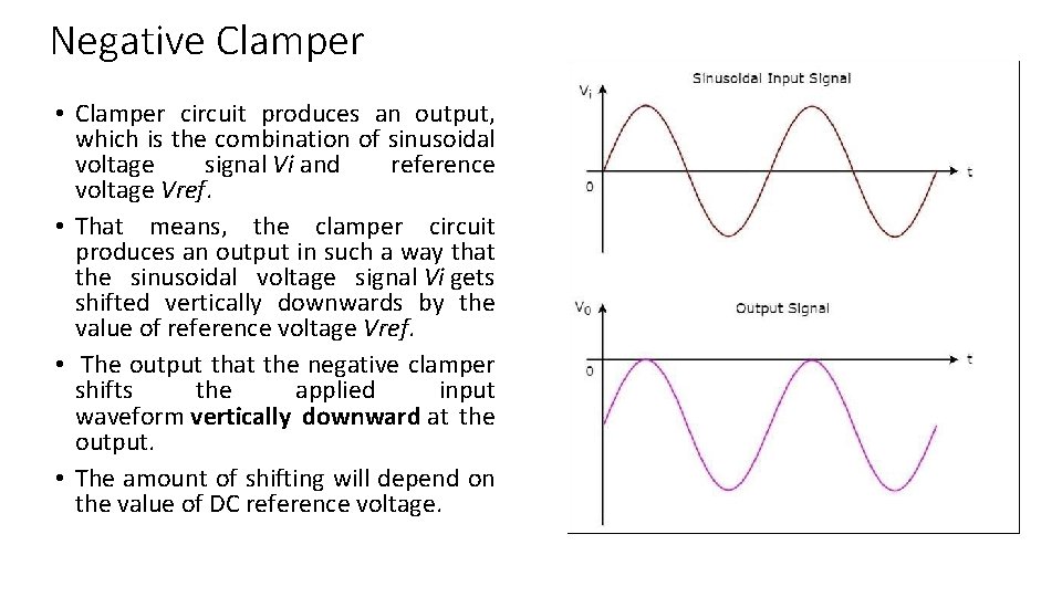
Negative Clamper • Clamper circuit produces an output, which is the combination of sinusoidal voltage signal Vi and reference voltage Vref. • That means, the clamper circuit produces an output in such a way that the sinusoidal voltage signal Vi gets shifted vertically downwards by the value of reference voltage Vref. • The output that the negative clamper shifts the applied input waveform vertically downward at the output. • The amount of shifting will depend on the value of DC reference voltage.

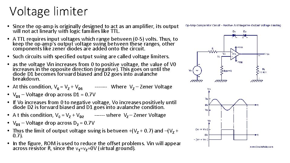
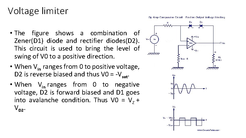
Voltage limiter • Since the op-amp is originally designed to act as an amplifier, its output will not act linearly with logic families like TTL. • A TTL requires input voltages which range between (0 -5) volts. Thus, to keep the op-amp’s output voltage swing between these ranges, other components like zener diodes are added onto the circuit. • Such circuits with specified output swing are called voltage limiters. • as the voltage Vin increases from 0 to positive voltage, the value of V 0 increases in the opposite direction (negative). This goes on until the diode D 1 becomes forward biased and D 2 goes into avalanche breakdown. • At this condition, V 0 = VZ + VD 1 ------- Where VZ – Zener Voltage • VD 1 – Voltage drop across D 1 = 0. 7 V • If Vo increases from 0 to negative voltage, Vo increases positively until diode D 2 is forward biased and D 1 goes into avalanche condition. • A t this condition, V 0 = VZ + VD 2 ------ where VZ – Zener Voltage • VD 1 – Voltage drop across D 2 = 0. 7 V • Thus the limit of output voltage swing is between +(VZ + 0. 7) and –(VZ + 0. 7). • In the figure, ROM is used to reduce the offset problems. Vin will appear across resistor R, since the v 1=v 2=0 V (virtual ground).

Voltage limiter • The figure shows a combination of Zener(D 1) diode and rectifier diodes(D 2). This circuit is used to bring the level of swing of V 0 to a positive direction. • When Vin ranges from 0 to positive voltage, D 2 is reverse biased and thus V 0 = -Vsat. • When Vin ranges from 0 to negative voltage, D 2 is forward biased and D 1 goes into avalanche condition. Thus V 0 = VZ + VD 2.

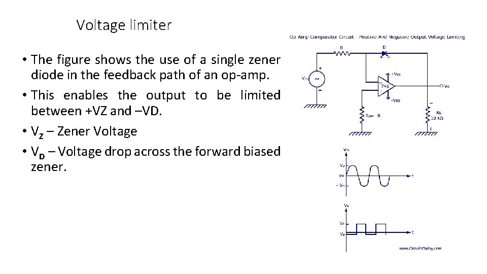
Voltage limiter • The figure shows the use of a single zener diode in the feedback path of an op-amp. • This enables the output to be limited between +VZ and –VD. • VZ – Zener Voltage • VD – Voltage drop across the forward biased zener.

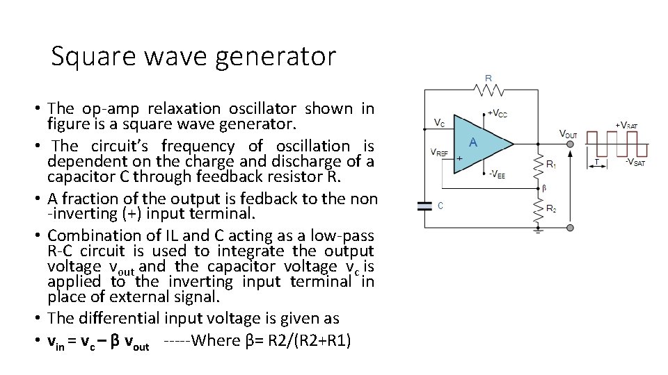
Square wave generator • The op-amp relaxation oscillator shown in figure is a square wave generator. • The circuit’s frequency of oscillation is dependent on the charge and discharge of a capacitor C through feedback resistor R. • A fraction of the output is fedback to the non -inverting (+) input terminal. • Combination of IL and C acting as a low-pass R-C circuit is used to integrate the output voltage vout and the capacitor voltage vc is applied to the inverting input terminal in place of external signal. • The differential input voltage is given as • vin = vc – β vout -----Where β= R 2/(R 2+R 1)

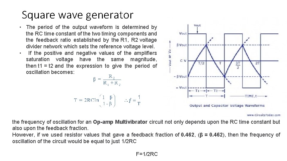
Square wave generator • The period of the output waveform is determined by the RC time constant of the two timing components and the feedback ratio established by the R 1, R 2 voltage divider network which sets the reference voltage level. • If the positive and negative values of the amplifiers saturation voltage have the same magnitude, then t 1 = t 2 and the expression to give the period of oscillation becomes: the frequency of oscillation for an Op-amp Multivibrator circuit not only depends upon the RC time constant but also upon the feedback fraction. However, if we used resistor values that gave a feedback fraction of 0. 462, (β = 0. 462), then the frequency of oscillation of the circuit would be equal to just 1/2 RC F=1/2 RC

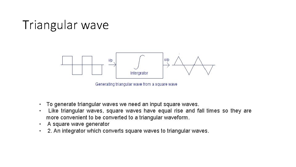
Triangular wave • To generate triangular waves we need an input square waves. • Like triangular waves, square waves have equal rise and fall times so they are more convenient to be converted to a triangular waveform. • A square wave generator • 2. An integrator which converts square waves to triangular waves.

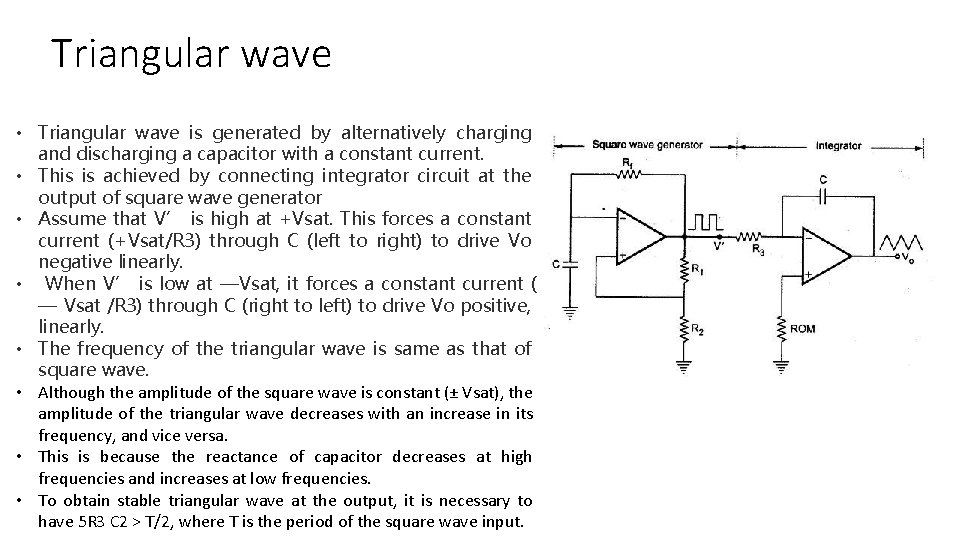
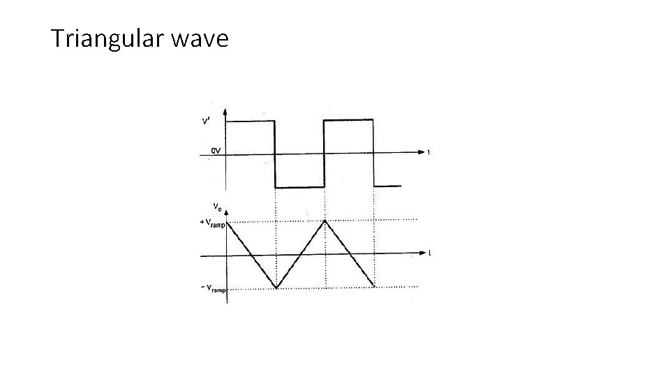
Triangular wave • Triangular wave is generated by alternatively charging and discharging a capacitor with a constant current. • This is achieved by connecting integrator circuit at the output of square wave generator • Assume that V’ is high at +Vsat. This forces a constant current (+Vsat/R 3) through C (left to right) to drive Vo negative linearly. • When V’ is low at —Vsat, it forces a constant current ( — Vsat /R 3) through C (right to left) to drive Vo positive, linearly. • The frequency of the triangular wave is same as that of square wave. • Although the amplitude of the square wave is constant (± Vsat), the amplitude of the triangular wave decreases with an increase in its frequency, and vice versa. • This is because the reactance of capacitor decreases at high frequencies and increases at low frequencies. • To obtain stable triangular wave at the output, it is necessary to have 5 R 3 C 2 > T/2, where T is the period of the square wave input.

Triangular wave

Precision Rectifier • The major limitation of conventional rectifiers is that it cannot rectify AC voltages below forward voltage drop VD (0. 7 V) of a diode. • The precision rectifier will make it possible to rectify input voltage of a very small magnitude even less than forward voltage drop of diode. • The diode can be used in AM detector where power is negligible and we want information in the signal. • Rectifier circuits used for circuit detection with op-amps are called precision rectifiers. • • Necessity of Op-Amp: In case of normal power rectifier input applied is much larger than 0. 7 V. When forward biased voltage is less than 0. 7 V, then diode is not conducting. Therefore Op-amp is used to help diode to conduct. The precision rectifiers are classified in two categories. 1. Precision HWR 2. Precision FWR

Precision Half wave Rectifier • The circuit functions as a non-inverting precision half– wave rectifier circuit. • If V is positive, the op-amp output V also becomes positive. • Then the closed loop condition is achieved for the op-amp and the output voltage V = Vi. • When Vi < 0, the voltage V becomes negative and the diode is reverse biased. • The loop is then broken and the output V = 0. 1 OA 0 0 A 0 • • Consider the open loop gain AOL of the op-amp is approximately 104 and the cut-in voltage Vγ is ≈ 0. 7 V. When the input voltage Vi > Vγ / AOL, the output of the op-amp VOA exceeds Vγ and the diode D conducts. Then the circuit acts like a voltage follower for input voltage level Vi > Vγ / AOL , (i. e. when Vi > 0. 7/104 = 70μV), and the V 0 follows the Vi during the positive half cycle for Vi higher than 70μV as shown in figure. When Vi is negative or less than Vγ / AOL, the op-amp output VOA becomes negative, and the diode becomes reverse biased. The loop is then broken, and the op-amp swings down to negative saturation. However, the output terminal is now isolated from both the input signal and the output of the op-amp terminal thus V 0 =0. No current is then delivered to the RL except for the small bias current of the op-amp and the reverse saturation current of the diode. • This circuit is an example of a non-linear circuit, in which linear operation is achieved over the remaining region (V i < 0).

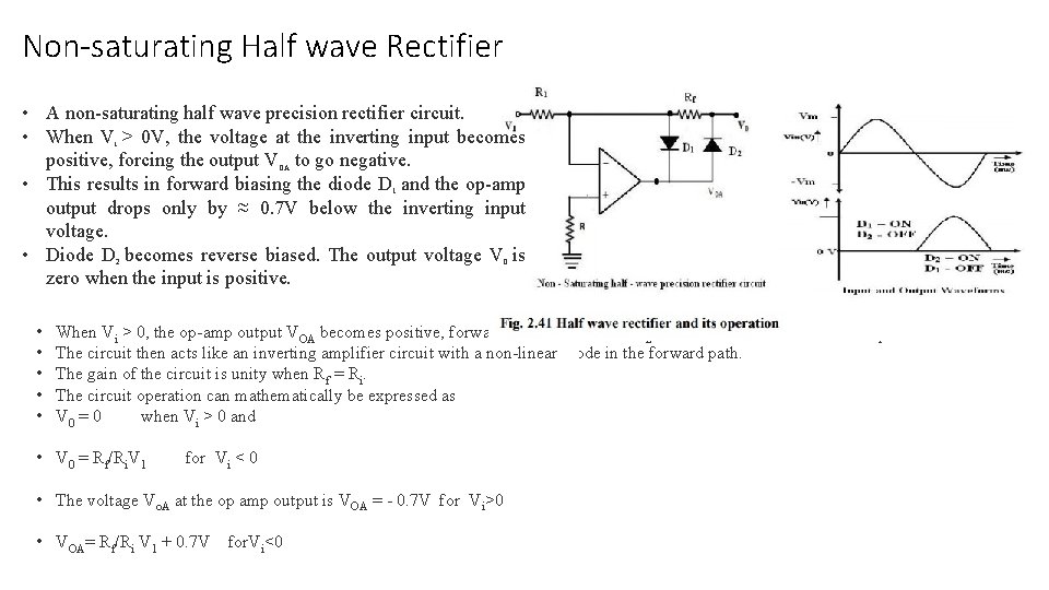
Non-saturating Half wave Rectifier • A non-saturating half wave precision rectifier circuit. • When V > 0 V, the voltage at the inverting input becomes positive, forcing the output V to go negative. • This results in forward biasing the diode D and the op-amp output drops only by ≈ 0. 7 V below the inverting input voltage. • Diode D becomes reverse biased. The output voltage V is zero when the input is positive. i OA 1 2 • • • 0 When Vi > 0, the op-amp output VOA becomes positive, forward biasing the diode D 2 and reverse biasing the diode D 1. The circuit then acts like an inverting amplifier circuit with a non-linear diode in the forward path. The gain of the circuit is unity when Rf = Ri. The circuit operation can mathematically be expressed as V 0 = 0 when Vi > 0 and • V 0 = Rf/Ri. V 1 for Vi < 0 • The voltage Vo. A at the op amp output is VOA = - 0. 7 V for Vi>0 • VOA= Rf/Ri V 1 + 0. 7 V for. Vi<0

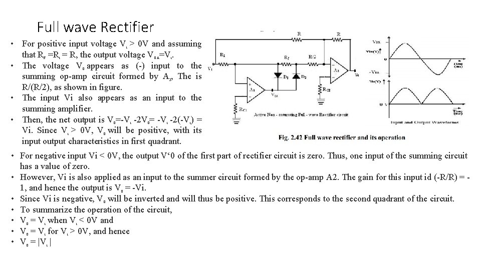
Full wave Rectifier • For positive input voltage V > 0 V and assuming that R =R = R, the output voltage V =V. • The voltage V appears as (-) input to the summing op-amp circuit formed by A , The is R/(R/2), as shown in figure. • The input Vi also appears as an input to the summing amplifier. • Then, the net output is V =-V -2 V = -V -2(-V ) = Vi. Since V > 0 V, V will be positive, with its input output characteristics in first quadrant. i F i OA i 0 2 0 i i 0 • For negative input Vi < 0 V, the output V‘ 0 of the first part of rectifier circuit is zero. Thus, one input of the summing circuit has a value of zero. • However, Vi is also applied as an input to the summer circuit formed by the op-amp A 2. The gain for this input id (-R/R) = 1, and hence the output is V = -Vi. • Since Vi is negative, V will be inverted and will thus be positive. This corresponds to the second quadrant of the circuit. • To summarize the operation of the circuit, • V = V when V < 0 V and • V = V for V > 0 V, and hence • V = |V | 0 0 0 i 0 i i i