Figure 3 1 Opamp equivalent circuit The two
- Slides: 19

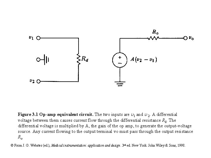
Figure 3. 1 Op-amp equivalent circuit. The two inputs are 1 and 2. A differential voltage between them causes current flow through the differential resistance Rd. The differential voltage is multiplied by A, the gain of the op amp, to generate the output-voltage source. Any current flowing to the output terminal vo must pass through the output resistance Ro. © From J. G. Webster (ed. ), Medical instrumentation: application and design. 3 rd ed. New York: John Wiley & Sons, 1998.

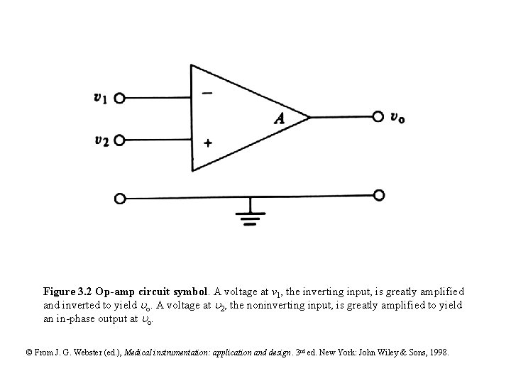
Figure 3. 2 Op-amp circuit symbol. A voltage at v 1, the inverting input, is greatly amplified and inverted to yield o. A voltage at 2, the noninverting input, is greatly amplified to yield an in-phase output at o. © From J. G. Webster (ed. ), Medical instrumentation: application and design. 3 rd ed. New York: John Wiley & Sons, 1998.

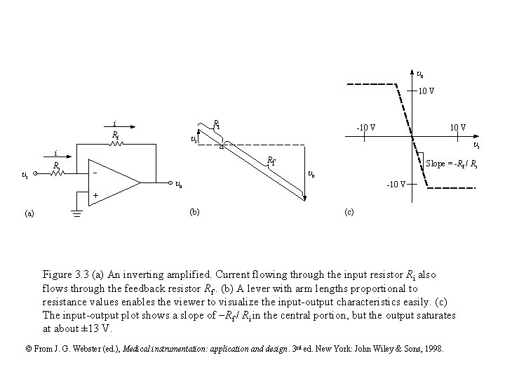
o 10 V i Rf Ri i Ri -10 V i Rf - o 10 V Slope = -Rf / Ri o -10 V + (a) (b) (c) Figure 3. 3 (a) An inverting amplified. Current flowing through the input resistor Ri also flows through the feedback resistor Rf. (b) A lever with arm lengths proportional to resistance values enables the viewer to visualize the input-output characteristics easily. (c) The input-output plot shows a slope of -Rf / Ri in the central portion, but the output saturates at about ± 13 V. © From J. G. Webster (ed. ), Medical instrumentation: application and design. 3 rd ed. New York: John Wiley & Sons, 1998.

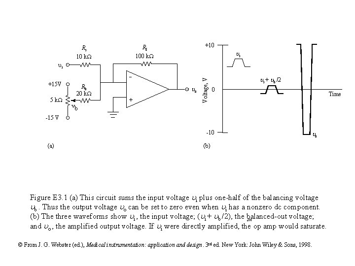
+10 Rf 100 k. W Ri 10 k. W i +15 V 5 k. W Rb 20 k. W vb o + Voltage, V i i + b /2 0 Time -15 V -10 (a) o (b) Figure E 3. 1 (a) This circuit sums the input voltage i plus one-half of the balancing voltage b. Thus the output voltage o can be set to zero even when i has a nonzero dc component. (b) The three waveforms show i , the input voltage; ( i + b /2), the balanced-out voltage; JH and o , the amplified output voltage. If i were directly amplified, the op amp would saturate. © From J. G. Webster (ed. ), Medical instrumentation: application and design. 3 rd ed. New York: John Wiley & Sons, 1998.

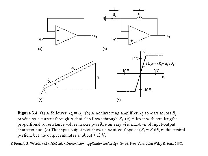
i i Ri Rf - - o i + (a) o i + (b) o 10 V Slope = (Rf + Ri )/ Ri Rf -10 V i o Ri i (c) 10 V -10 V (d) Figure 3. 4 (a) A follower, o = i. (b) A noninverting amplifier, i appears across Ri , producing a current through Ri that also flows through Rf. (c) A lever with arm lengths proportional to resistance values makes possible an easy visualization of input-output characteristic. (d) The input-output plot shows a positive slope of (Rf + Ri)/Ri in the central portion, but the output saturates at about ± 13 V. © From J. G. Webster (ed. ), Medical instrumentation: application and design. 3 rd ed. New York: John Wiley & Sons, 1998.

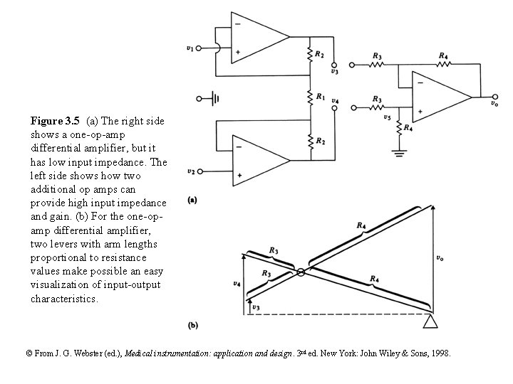
Figure 3. 5 (a) The right side shows a one-op-amp differential amplifier, but it has low input impedance. The left side shows how two additional op amps can provide high input impedance and gain. (b) For the one-opamp differential amplifier, two levers with arm lengths proportional to resistance values make possible an easy visualization of input-output characteristics. © From J. G. Webster (ed. ), Medical instrumentation: application and design. 3 rd ed. New York: John Wiley & Sons, 1998.

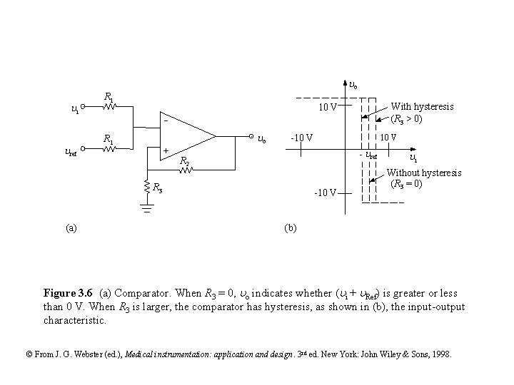
o i ref R 1 - o R 1 + -10 V - ref R 2 R 3 (a) With hysteresis (R 3 > 0) 10 V -10 V i Without hysteresis (R 3 = 0) (b) Figure 3. 6 (a) Comparator. When R 3 = 0, o indicates whether ( i + Ref) is greater or less than 0 V. When R 3 is larger, the comparator has hysteresis, as shown in (b), the input-output characteristic. © From J. G. Webster (ed. ), Medical instrumentation: application and design. 3 rd ed. New York: John Wiley & Sons, 1998.

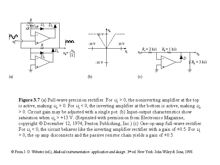
R x. R (1 -x)R D 1 D 2 o - i + 10 V -10 V R D 4 - D 3 o= 10 V i i x i Ri = 2 k. W - -10 V + (a) Rf = 1 k. W D vo RL = 3 k. W + (b) (c) Figure 3. 7 (a) Full-wave precision rectifier. For i > 0, the noninverting amplifier at the top is active, making o > 0. For i < 0, the inverting amplifier at the bottom is active, making o > 0. Circuit gain may be adjusted with a single pot. (b) Input-output characteristics show saturation when o > +13 V. (Reprinted with permission from Electronics Magazine, copyright December 12, 1974; Penton Publishing, Inc. ) (c) One-op-amp full-wave rectifier. For i < 0, the circuit behaves like the inverting amplifier rectifier with a gain of +0. 5. For i > 0, the op amp disconnects and the passive resistor chain yields a gain of +0. 5. © From J. G. Webster (ed. ), Medical instrumentation: application and design. 3 rd ed. New York: John Wiley & Sons, 1998.

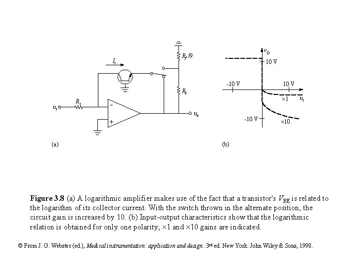
Ic vo Rf /9 10 V -10 V Rf i Ri 1 - o -10 V + (a) 10 V i 10 (b) Figure 3. 8 (a) A logarithmic amplifier makes use of the fact that a transistor's VBE is related to the logarithm of its collector current. With the switch thrown in the alternate position, the circuit gain is increased by 10. (b) Input-output characteristics show that the logarithmic relation is obtained for only one polarity; 1 and 10 gains are indicated. © From J. G. Webster (ed. ), Medical instrumentation: application and design. 3 rd ed. New York: John Wiley & Sons, 1998.

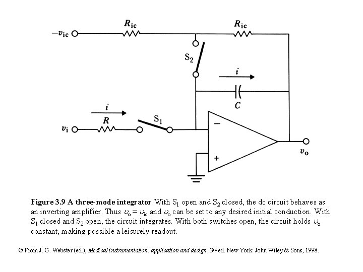
Figure 3. 9 A three-mode integrator With S 1 open and S 2 closed, the dc circuit behaves as an inverting amplifier. Thus o = ic and o can be set to any desired initial conduction. With S 1 closed and S 2 open, the circuit integrates. With both switches open, the circuit holds o constant, making possible a leisurely readout. © From J. G. Webster (ed. ), Medical instrumentation: application and design. 3 rd ed. New York: John Wiley & Sons, 1998.

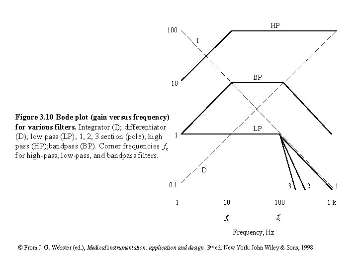
HP 100 I BP 10 Figure 3. 10 Bode plot (gain versus frequency) for various filters. Integrator (I); differentiator 1 (D); low pass (LP), 1, 2, 3 section (pole); high pass (HP); bandpass (BP). Corner frequencies fc for high-pass, low-pass, and bandpass filters. LP D 0. 1 1 3 10 100 fc fc 2 Frequency, Hz © From J. G. Webster (ed. ), Medical instrumentation: application and design. 3 rd ed. New York: John Wiley & Sons, 1998. 1 1 k

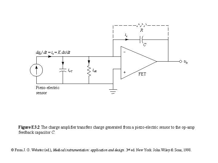
is R C - dqs/ dt = is = K dx/dt o is. C is. R + FET Piezo-electric sensor Figure E 3. 2 The charge amplifier transfers charge generated from a piezo-electric sensor to the op-amp feedback capacitor C. © From J. G. Webster (ed. ), Medical instrumentation: application and design. 3 rd ed. New York: John Wiley & Sons, 1998.

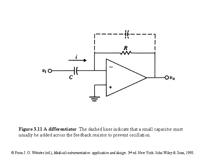
Figure 3. 11 A differentiator The dashed lines indicate that a small capacitor must usually be added across the feedback resistor to prevent oscillation. © From J. G. Webster (ed. ), Medical instrumentation: application and design. 3 rd ed. New York: John Wiley & Sons, 1998.

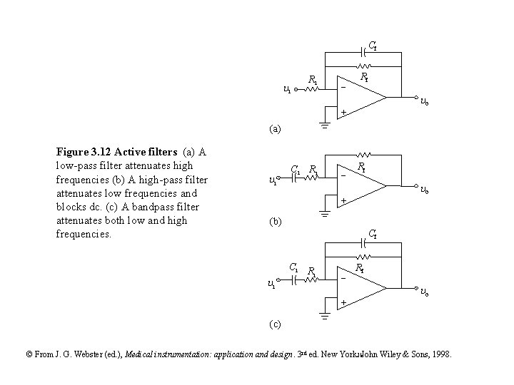
Cf i Ri - Rf o + (a) Figure 3. 12 Active filters (a) A low-pass filter attenuates high frequencies (b) A high-pass filter attenuates low frequencies and blocks dc. (c) A bandpass filter attenuates both low and high frequencies. i Ci Ri - Rf o + (b) Cf i Ci R i + Rf o (c) © From J. G. Webster (ed. ), Medical instrumentation: application and design. 3 rd ed. New York: JHJohn Wiley & Sons, 1998.

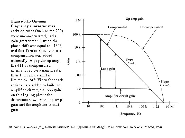
Figure 3. 13 Op-amp frequency characteristics early op amps (such as the 709) were uncompensated, had a gain greater than 1 when the phase shift was equal to – 180º, and therefore oscillated unless compensation was added externally. A popular op amp, the 411, is compensated internally, so for a gain greater than 1, the phase shift is limited to – 90º. When feedback resistors are added to build an amplifier circuit, the loop gain on this log-log plot is the difference between the op-amp gain and the amplifier-circuit gain. © From J. G. Webster (ed. ), Medical instrumentation: application and design. 3 rd ed. New York: John Wiley & Sons, 1998.

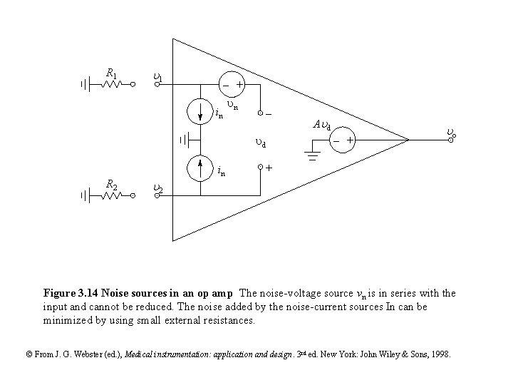
R 1 1 - + in n d R 2 in A d - + o + 2 Figure 3. 14 Noise sources in an op amp The noise-voltage source vn is in series with the input and cannot be reduced. The noise added by the noise-current sources In can be minimized by using small external resistances. © From J. G. Webster (ed. ), Medical instrumentation: application and design. 3 rd ed. New York: John Wiley & Sons, 1998.

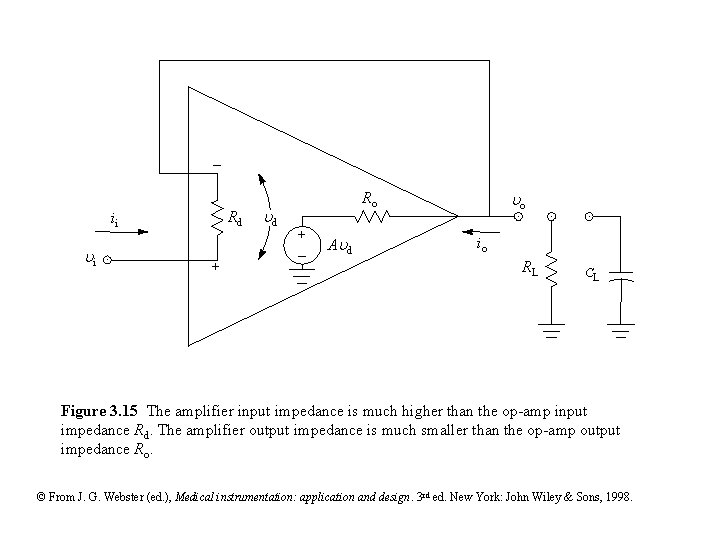
Rd ii i + d o Ro + - A d io RL CL Figure 3. 15 The amplifier input impedance is much higher than the op-amp input impedance Rd. The amplifier output impedance is much smaller than the op-amp output impedance Ro. © From J. G. Webster (ed. ), Medical instrumentation: application and design. 3 rd ed. New York: John Wiley & Sons, 1998.

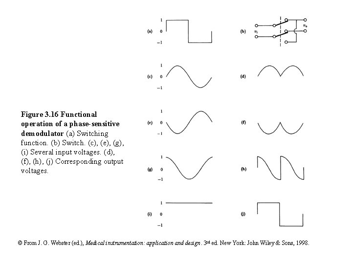
Figure 3. 16 Functional operation of a phase-sensitive demodulator (a) Switching function. (b) Switch. (c), (e), (g), (i) Several input voltages. (d), (f), (h), (j) Corresponding output voltages. © From J. G. Webster (ed. ), Medical instrumentation: application and design. 3 rd ed. New York: John Wiley & Sons, 1998.

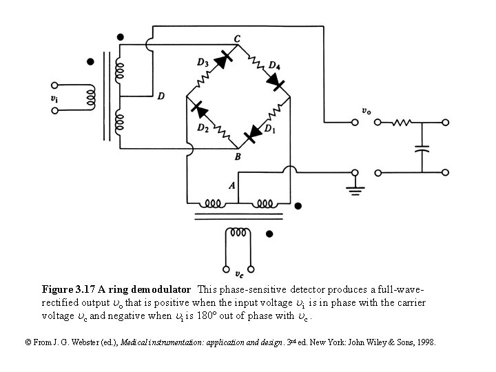
Figure 3. 17 A ring demodulator This phase-sensitive detector produces a full-waverectified output o that is positive when the input voltage i is in phase with the carrier voltage c and negative when i is 180º out of phase with c. © From J. G. Webster (ed. ), Medical instrumentation: application and design. 3 rd ed. New York: John Wiley & Sons, 1998.