TUTORIAL I DEVICE PHYSICS CHARGE TRANSPORT APPLICATIONS AND
![Models for Contact injection: [1] V. I. Arkhipov, E. V. Emelianova, Y. H. Tak, Models for Contact injection: [1] V. I. Arkhipov, E. V. Emelianova, Y. H. Tak,](https://slidetodoc.com/presentation_image_h/a0ee424872dd406d90a2c0adad3370f2/image-48.jpg)
![Transport models [1] [2] [3] [4] [5] [6] [7] [8] [9] [10] [11] [12] Transport models [1] [2] [3] [4] [5] [6] [7] [8] [9] [10] [11] [12]](https://slidetodoc.com/presentation_image_h/a0ee424872dd406d90a2c0adad3370f2/image-49.jpg)
![Transport in FETs [1] [2] [3] [4] [5] [6] [7] [8] [9] [10] [11] Transport in FETs [1] [2] [3] [4] [5] [6] [7] [8] [9] [10] [11]](https://slidetodoc.com/presentation_image_h/a0ee424872dd406d90a2c0adad3370f2/image-50.jpg)
- Slides: 57

TUTORIAL I DEVICE PHYSICS, CHARGE TRANSPORT, APPLICATIONS AND PROCESSING IN ORGANIC ELECTRONICS Nir Tessler Devin Mackenzie March 28, 2005 1: 30 – 5: 00 PM 1

MRS SPRING 2005 TUTORIAL I DEVICE PHYSICS, CHARGE TRANSPORT, APPLICATIONS AND PROCESSING IN ORGANIC ELECTRONICS PART 1 DEVICE PHYSICS and CHARGE TRANSPORT Nir Tessler EE Dept. Technion www. ee. technion. ac. il/nir 2

Organic Semiconductors Nir Tessler, EE Dept. Technion www. ee. technion. ac. il/nir 1. Semiconductor 2. High band gap 3. Low mobility 4. Molecular You are holding ~60 slides but we will look together only at part of them. Watch for the slide number 3

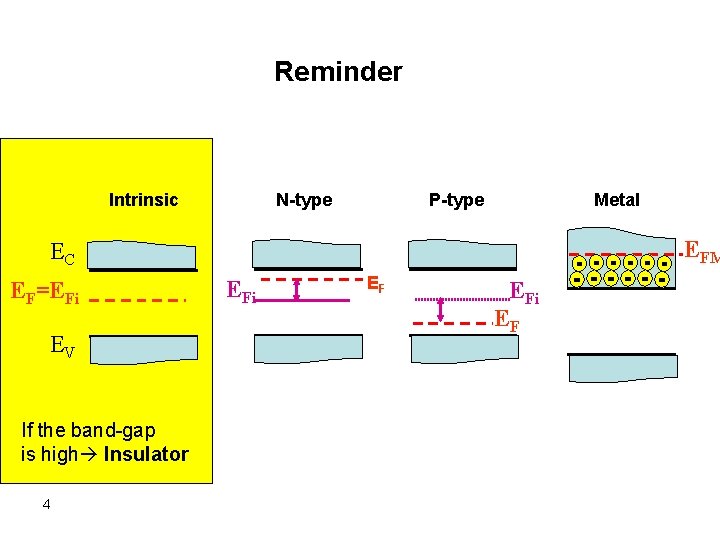
Reminder N-type Intrinsic P-type Metal EFM EC EF=EFi EV If the band-gap is high Insulator 4 EFi EF

Semiconductor 5

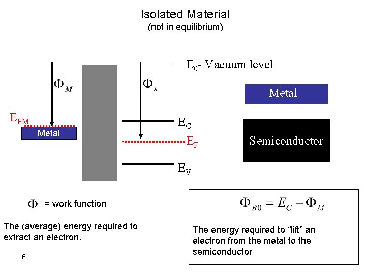
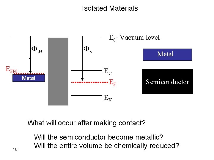
Isolated Material (not in equilibrium) E 0 - Vacuum level Metal EFM Metal EC EF Semiconductor EV = work function The (average) energy required to extract an electron. 6 The energy required to “lift” an electron from the metal to the semiconductor

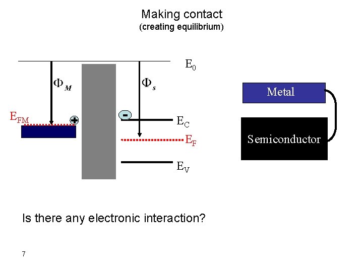
Making contact (creating equilibrium) E 0 Metal EFM EC EF EV Is there any electronic interaction? 7 Semiconductor

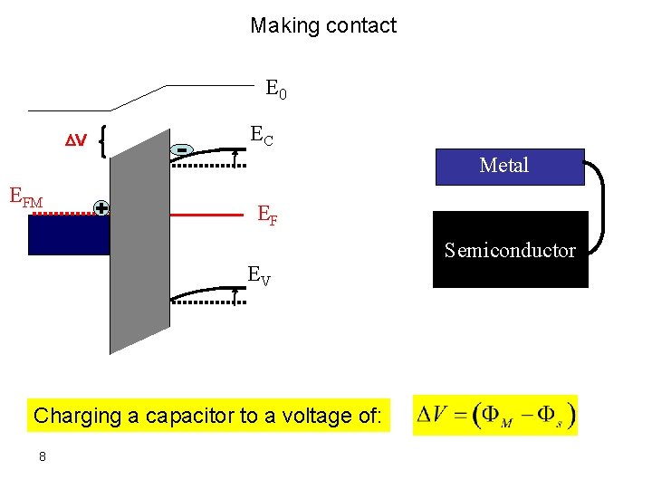
Making contact E 0 DV EC Metal EFM EF EV Charging a capacitor to a voltage of: 8 Semiconductor

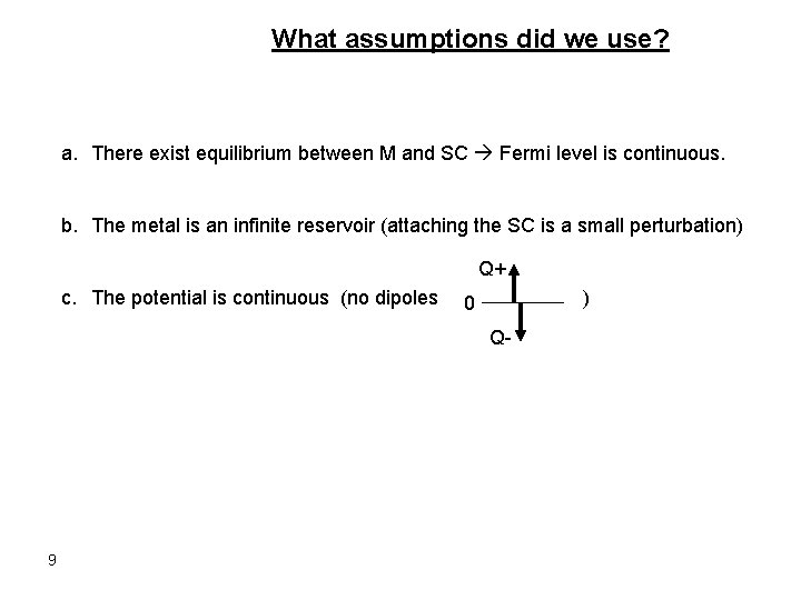
What assumptions did we use? a. There exist equilibrium between M and SC Fermi level is continuous. b. The metal is an infinite reservoir (attaching the SC is a small perturbation) Q+ c. The potential is continuous (no dipoles ) 0 Q- 9

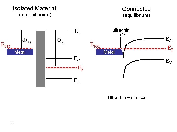
Isolated Materials E 0 - Vacuum level Metal EFM Metal EC EF Semiconductor EV What will occur after making contact? 10 Will the semiconductor become metallic? Will the entire volume be chemically reduced?

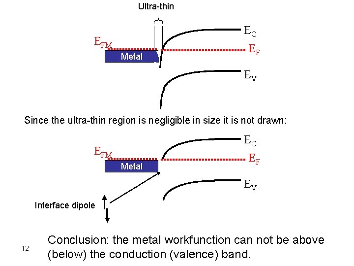
Isolated Material Connected (no equilibrium) (equilibrium) E 0 ultra-thin EC EFM Metal EC EV EF EV Ultra-thin ~ nm scale 11 EF

Ultra-thin EC EFM Metal EF EV Since the ultra-thin region is negligible in size it is not drawn: EC EFM Metal EF EV Interface dipole 12 Conclusion: the metal workfunction can not be above (below) the conduction (valence) band.

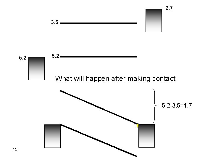
2. 7 3. 5 5. 2 What will happen after making contact 5. 2 -3. 5=1. 7 13

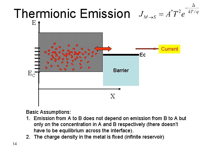
Thermionic Emission E Ec EC Current Barrier X Basic Assumptions: 1. Emission from A to B does not depend on emission from B to A but only on the concentration in A and B respectively (there doesn’t have to be equilibrium across the interface). 2. The charge density in the metal is fixed (infinite reservoir) 14

In Low mobility semiconductors (organics) the emission rates from metal to organic and back are much larger then the current flowing in the device: 1. There is equilibrium at the contact interface 2. The thermionic emission process is not important but for ensuring equilibrium. What may change the above? What may slow the emission across the interface? The presence of a thin insulating layer will make the crossing from the metal to the organic (tunneling) very slow and it will become the rate limiting factor (i. e. break the equilibrium). 15

Now the charges are in • How do they move? 22

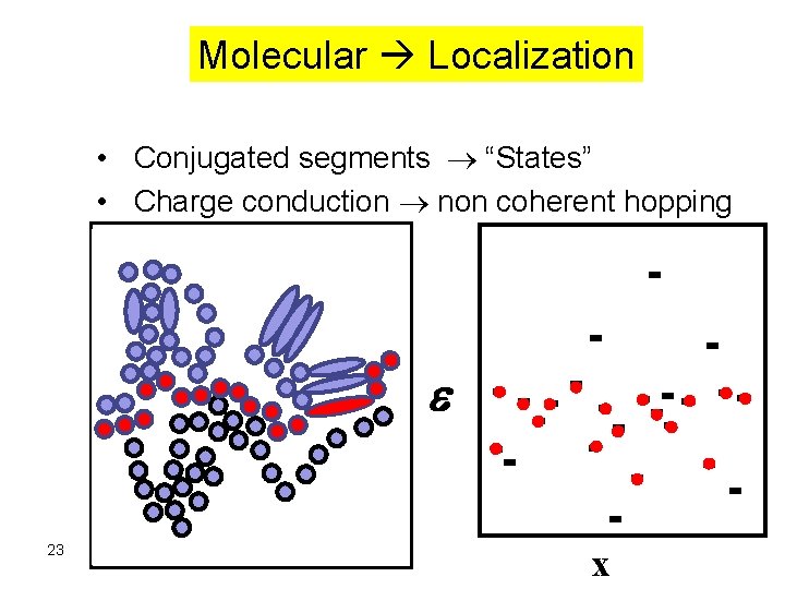
Molecular Localization • Conjugated segments “States” • Charge conduction non coherent hopping e 23 x

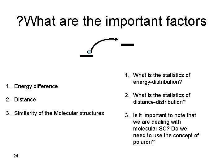
? What are the important factors 1. Energy difference 2. Distance 3. Similarity of the Molecular structures 24 1. What is the statistics of energy-distribution? 2. What is the statistics of distance-distribution? 3. Is it important to note that we are dealing with molecular SC? Do we need to use the concept of polaron?

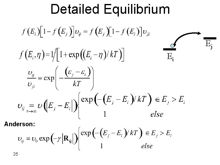
Detailed Equilibrium Ej Ei Anderson: 25

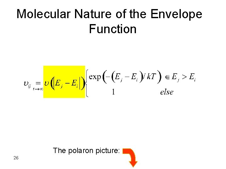
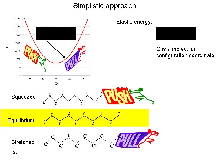
Molecular Nature of the Envelope Function The polaron picture: 26

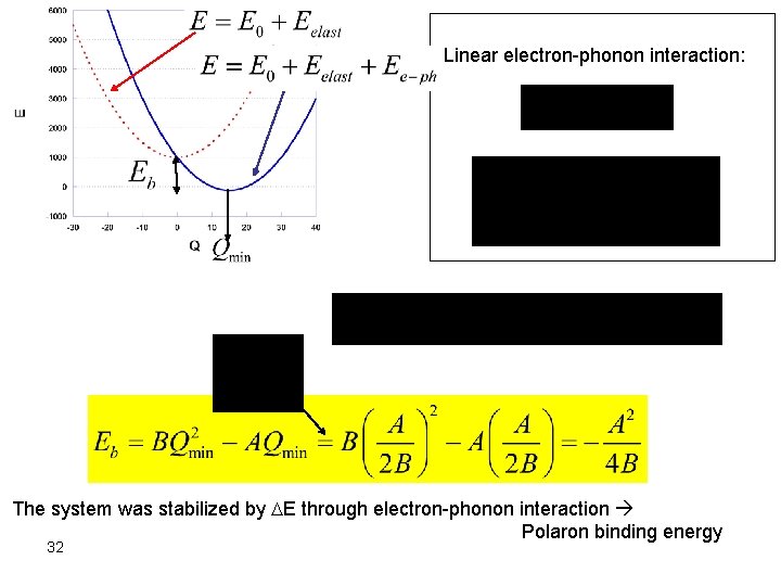
Simplistic approach Elastic energy: Q is a molecular configuration coordinate Squeezed Equilibrium Stretched 27

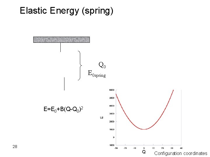
Elastic Energy (spring) Q 0 E 0 spring E=E 0+B(Q-Q 0)2 28 Configuration coordinates

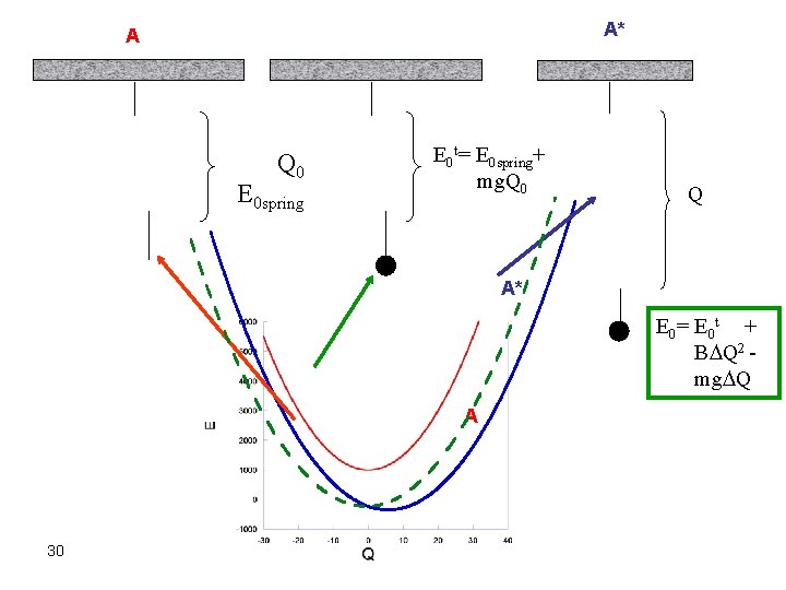
A* A Q 0 E 0 spring E 0 t= E 0 spring+ mg. Q 0 Q A* E 0 = E 0 t + BDQ 2 mg. DQ A 30

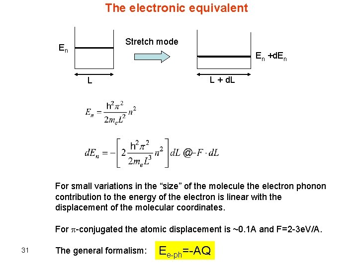
The electronic equivalent Stretch mode En En +d. En L L + d. L For small variations in the “size” of the molecule the electron phonon contribution to the energy of the electron is linear with the displacement of the molecular coordinates. For p-conjugated the atomic displacement is ~0. 1 A and F=2 -3 e. V/A. 31 The general formalism: Ee-ph=-AQ

Linear electron-phonon interaction: The system was stabilized by DE through electron-phonon interaction Polaron binding energy 32

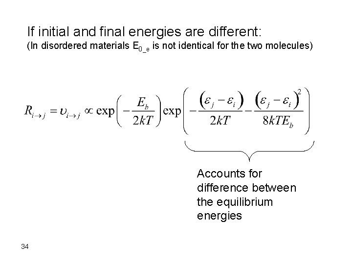
If initial and final energies are different: (In disordered materials E 0_e is not identical for the two molecules) Accounts for difference between the equilibrium energies 34

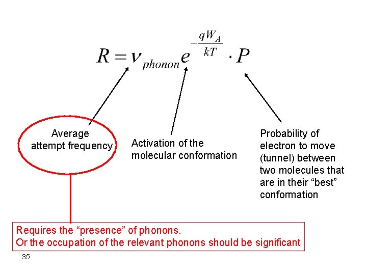
Average attempt frequency Activation of the molecular conformation Probability of electron to move (tunnel) between two molecules that are in their “best” conformation Requires the “presence” of phonons. Or the occupation of the relevant phonons should be significant 35

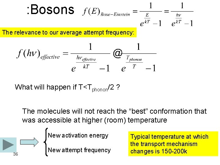
: Bosons The relevance to our average attempt frequency: What will happen if T<Tphonon/2 ? The molecules will not reach the “best” conformation that was accessible at higher (room) temperature New activation energy 36 New attempt frequency Typical temperature at which the transport mechanism changes is 150 -200 k

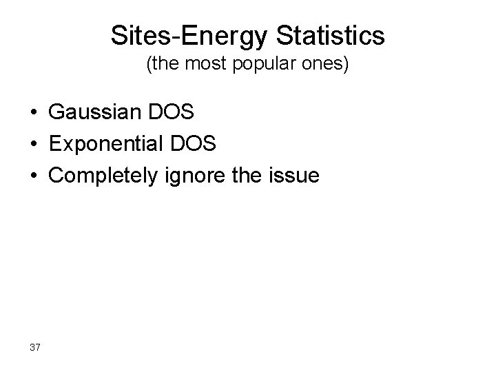
Sites-Energy Statistics (the most popular ones) • Gaussian DOS • Exponential DOS • Completely ignore the issue 37

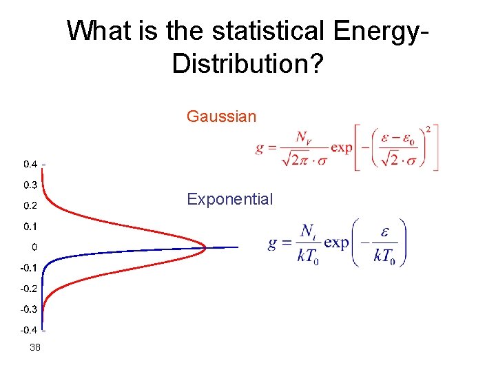
What is the statistical Energy. Distribution? Gaussian Exponential 38

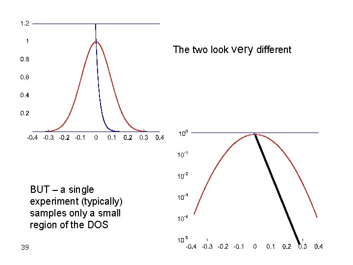
The two look very different BUT – a single experiment (typically) samples only a small region of the DOS 39

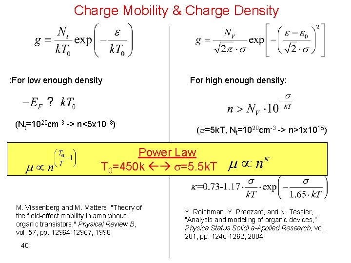
Charge Mobility & Charge Density : For low enough density (Nt=1020 cm-3 -> n<5 x 10¹⁸) For high enough density: (s=5 k. T, Nt=1020 cm-3 -> n>1 x 10¹⁵) Power Law T 0=450 k s=5. 5 k. T M. Vissenberg and M. Matters, "Theory of the field-effect mobility in amorphous organic transistors, " Physical Review B, vol. 57, pp. 12964 -12967, 1998 40 Y. Roichman, Y. Preezant, and N. Tessler, "Analysis and modeling of organic devices, " Physica Status Solidi a-Applied Research, vol. 201, pp. 1246 -1262, 2004

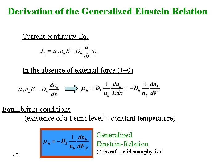
Derivation of the Generalized Einstein Relation Current continuity Eq. In the absence of external force (J=0) Equilibrium conditions (existence of a Fermi level + constant temperature) Generalized Einstein-Relation 42 (Ashcroft, solid state physics)

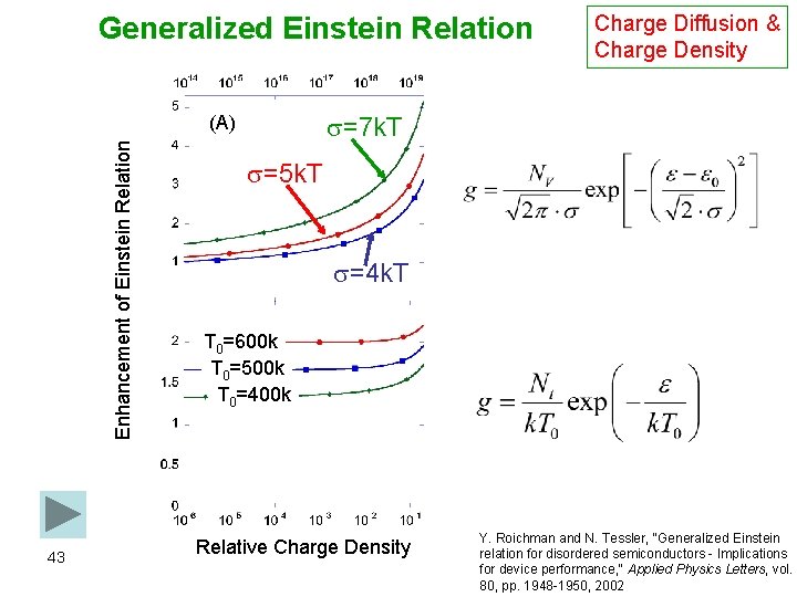
Generalized Einstein Relation s=7 k. T Enhancement of Einstein Relation (A) 43 Charge Diffusion & Charge Density s=5 k. T s=4 k. T T 0=600 k T 0=500 k T 0=400 k Relative Charge Density Y. Roichman and N. Tessler, "Generalized Einstein relation for disordered semiconductors - Implications for device performance, " Applied Physics Letters, vol. 80, pp. 1948 -1950, 2002

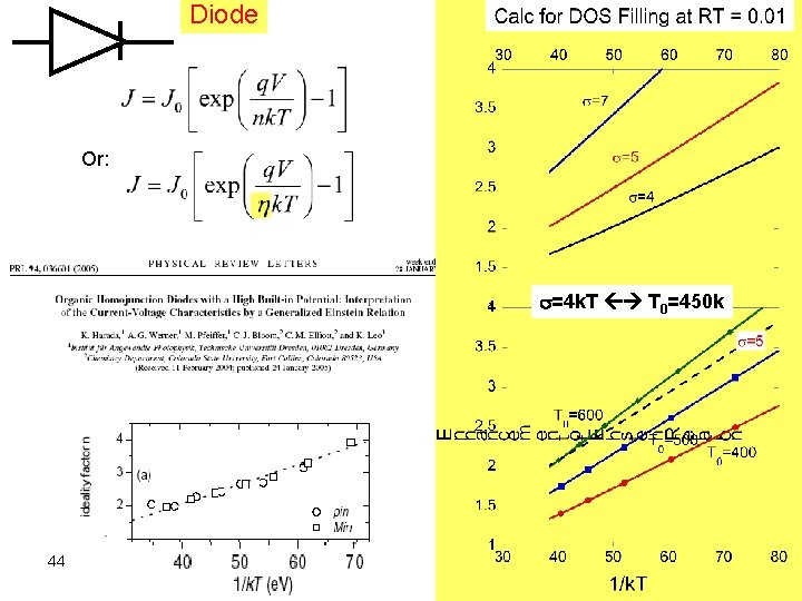
Diode Or: s=4 k. T T 0=450 k 44

Extracting Mobility • Analysis of LEDs • Analysis of FETs The disorder parameter s is an established important feature Can we extract it? 45

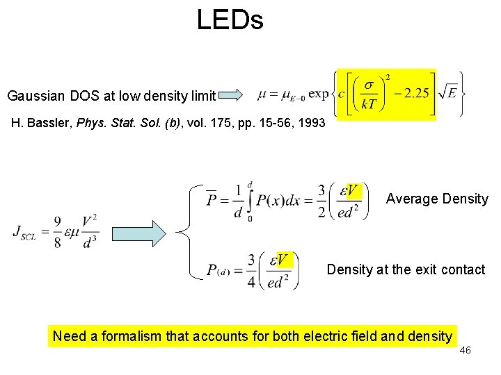
LEDs Gaussian DOS at low density limit H. Bassler, Phys. Stat. Sol. (b), vol. 175, pp. 15 -56, 1993 Average Density at the exit contact Need a formalism that accounts for both electric field and density 46

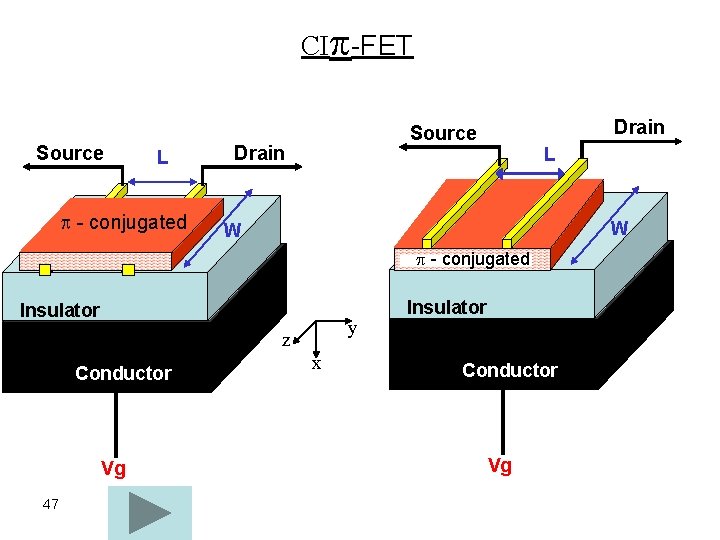
CIp-FET Source L p - conjugated Drain Source Drain L W W p - conjugated L Si. O 2 Insulator y z Si Conductor Vg 47 x L Si. O 2 Insulator Si Conductor Vg

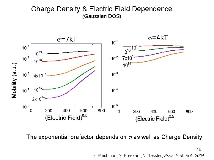
Charge Density & Electric Field Dependence (Gaussian DOS) s=4 k. T Mobility (a. u. ) s=7 k. T The exponential prefactor depends on s as well as Charge Density 48 Y. Roichman, Y. Preezant, N. Tessler, Phys. Stat. Sol. 2004

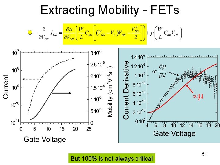
Extracting Mobility - FETs But 100% is not always critical 51

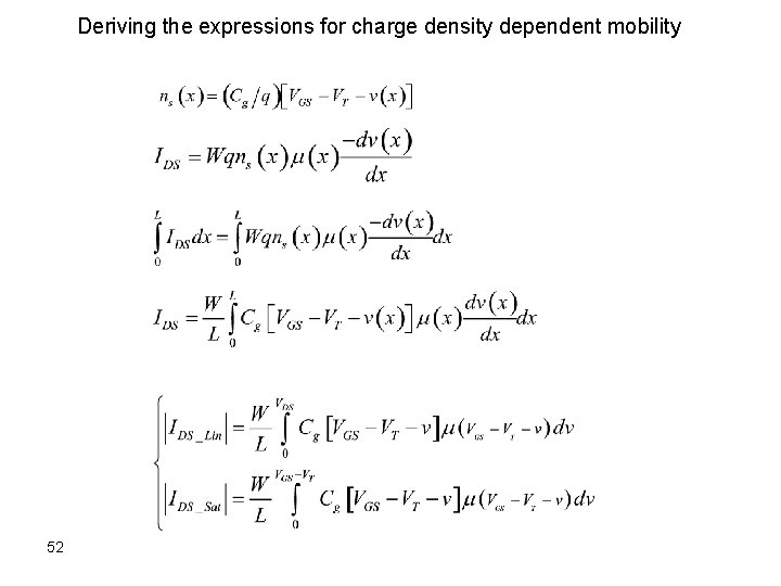
Deriving the expressions for charge density dependent mobility 52

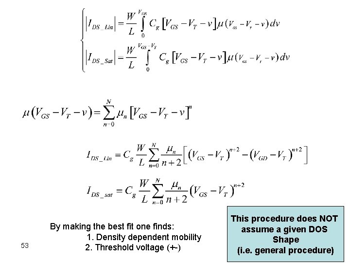
53 By making the best fit one finds: 1. Density dependent mobility 2. Threshold voltage (+-) This procedure does NOT assume a given DOS Shape (i. e. general procedure)

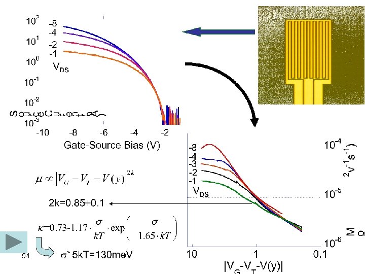
54

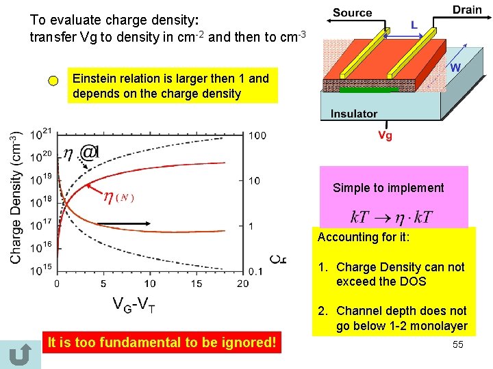
To evaluate charge density: transfer Vg to density in cm-2 and then to cm-3 Einstein relation is larger then 1 and depends on the charge density Simple to implement Accounting for it: 1. Charge Density can not exceed the DOS 2. Channel depth does not go below 1 -2 monolayer It is too fundamental to be ignored! 55

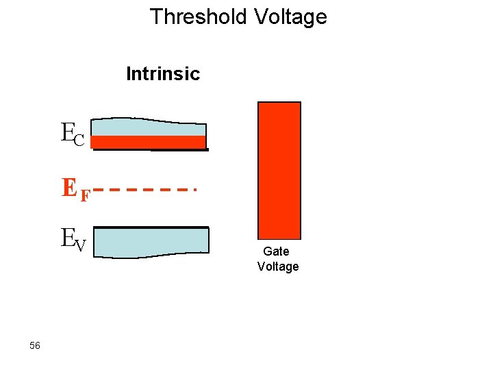
Threshold Voltage Intrinsic EC EF EV 56 Gate Voltage

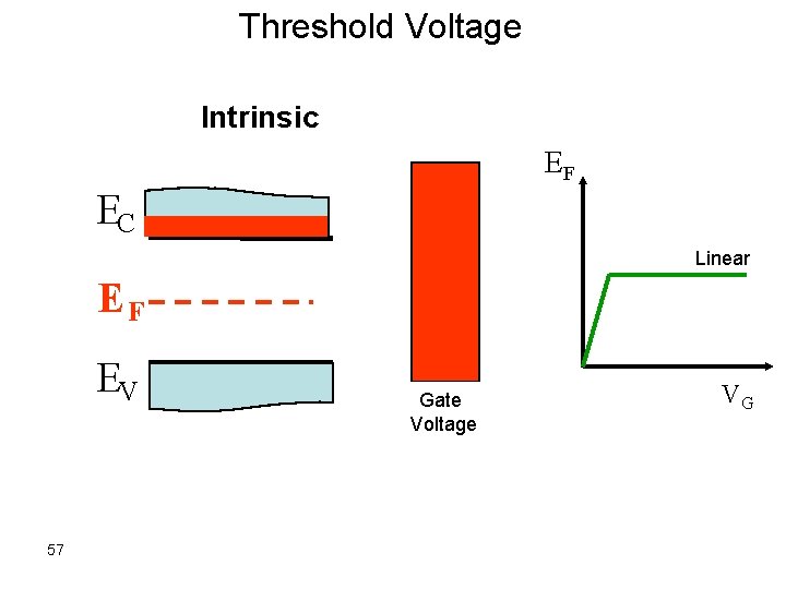
Threshold Voltage Intrinsic EF EC Linear EF EV 57 Gate Voltage VG

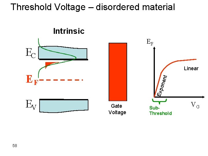
Threshold Voltage – disordered material Intrinsic EF EC Linear EV 58 Exp on ent EF Gate Voltage Sub. Threshold VG
![Models for Contact injection 1 V I Arkhipov E V Emelianova Y H Tak Models for Contact injection: [1] V. I. Arkhipov, E. V. Emelianova, Y. H. Tak,](https://slidetodoc.com/presentation_image_h/a0ee424872dd406d90a2c0adad3370f2/image-48.jpg)
Models for Contact injection: [1] V. I. Arkhipov, E. V. Emelianova, Y. H. Tak, and H. Bassler, "Charge injection into light-emitting diodes: Theory and experiment, " Journal of Applied Physics, vol. 84, pp. 848 -856, 1998. [2] V. I. Arkhipov, U. Wolf, and H. Bassler, "Current injection from metal to disordered hopping system. II. Comparison between analytic theory and simulation, " Phys. Rev. B, vol. 59, pp. 7514 -7520, 1999 [3] M. A. Baldo and S. R. Forrest, "Interface-limited injection in amorphous organic semiconductors - art. no. 085201, " Physical Review B, vol. 6408, pp. 5201 -+, 2001. [4] M. A. Baldo, Z. G. Soos, and S. R. Forrest, "Local order in amorphous organic molecular thin f ilms, " Chemical Physics Letters, vol. 347, pp. 297 -303, 2001 [5] Y. Preezant and N. Tessler, "Self-consistent analysis of the contact phenomena in lowmobility semiconductors, " Journal of Applied Physics, vol. 93, pp. 2059 - 2064, 2003. [6] Y. Preezant, Y. Roichman, and N. Tessler, "Amorphous Organic Devices Degenerate Semiconductors, " J. Phys. Cond. Matt. , vol. 14, pp. 9913– 9924, 2002. [7] Y. Roichman, Y. Preezant, and N. Tessler, "Analysis and modeling of organic devices, " Physica Status Solidi a-Applied Research, vol. 201, pp. 1246 -1262, 2004 [8] J. C. Scott and G. G. Malliaras, "Charge injection and recombination at the metal-organic interface, " Chemical Physics Letters, vol. 299, pp. 115 -119, 1999. [9] T. van Woudenbergh, P. W. M. Blom, M. Vissenberg, and J. N. Huiberts, "Temperature dependence of the charge injection in poly-dialkoxy-p-phenylene vinylene, " Applied Physics Letters, vol. 79, pp. 1697 -1699, 2001 [10] J. H. Werner and H. H. Guttler, "Barrier Inhomogeneities at Schottky Contacts, " Journal of Applied Physics, vol. 69, pp. 1522 -1533, 1991 59
![Transport models 1 2 3 4 5 6 7 8 9 10 11 12 Transport models [1] [2] [3] [4] [5] [6] [7] [8] [9] [10] [11] [12]](https://slidetodoc.com/presentation_image_h/a0ee424872dd406d90a2c0adad3370f2/image-49.jpg)
Transport models [1] [2] [3] [4] [5] [6] [7] [8] [9] [10] [11] [12] [13] [14] [15] [16] [17] 60 W. D. Gill, "Drift mobilities in amorphous charge-transfer complexes of trinitrofluorenone and poly-nvinylcarbazole, " J. Appl. Phys. , vol. 43, pp. 5033, 1972. M. Van der Auweraer, F. C. Deschryver, P. M. Borsenberger, and H. Bassler, "Disorder in Charge-Transport in Doped Polymers, " Advanced Materials, vol. 6, pp. 199 -213, 1994. R. Richert, L. Pautmeier, and H. Bassler, "Diffusion and drift of charge-carriers in a random potential deviation from einstein law, " Phys. Rev. Lett. , vol. 63, pp. 547 -550, 1989. V. I. Arkhipov, P. Heremans, E. V. Emelianova, G. J. Adriaenssens, and H. Bassler, "Weak-field carrier hopping in disordered organic semiconductors: the effects of deep traps and partly filled density-of-states distribution, " Journal of Physics-Condensed Matter, vol. 14, pp. 9899 -9911, 2002. M. Vissenberg and M. Matters, "Theory of the field-effect mobility in amorphous organic transistors, " Physical Review B, vol. 57, pp. 12964 -12967, 1998. D. Monroe, "Hopping in Exponential Band Tails, " Phys. Rev. Lett. , vol. 54, pp. 146 -149, 1985. H. Scher, M. F. Shlesinger, and J. T. Bendler, "TIME-SCALE INVARIANCE IN TRANSPORT AND RELAXATION, " Physics Today, vol. 44, pp. 26 -34, 1991. H. Scher and E. M. Montroll, "Anomalous transit-time dispersion in amorphous solids, " Phys. Rev. B, vol. 12, pp. 2455– 2477, 1975. E. M. Horsche, D. Haarer, and H. Scher, "Transition from dispersive to nondispersive transport: Photoconduction of polyvinylcarbazole, " Phys. Rev. B, vol. 35, pp. 1273 -1280, 1987. Y. Roichman, Y. Preezant, and N. Tessler, "Analysis and modeling of organic devices, " Physica Status Solidi a. Applied Research, vol. 201, pp. 1246 -1262, 2004. Y. Roichman and N. Tessler, "Generalized Einstein relation for disordered semiconductors - Implications for device performance, " Applied Physics Letters, vol. 80, pp. 1948 -1950, 2002. Y. N. Gartstein and E. M. Conwell, "High-Field Hopping Mobility in Molecular-Systems with Spatially Correlated Energetic Disorder, " Chemical Physics Letters, vol. 245, pp. 351 -358, 1995. H. C. F. Martens, P. W. M. Blom, and H. F. M. Schoo, "Comparative study of hole transport in poly(pphenylene vinylene) derivatives, " Physical Review B, vol. 61, pp. 7489 -7493, 2000 S. V. Rakhmanova and E. M. Conwell, "Electric-field dependence of mobility in conjugated polymer films, " Applied Physics Letters, vol. 76, pp. 3822 -3824, 2000 R. A. Marcus, "Chemical + Electrochemical Electron-Transfer Theory, " Annual Review of Physical Chemistry, vol. 15, pp. 155 -&, 1964. R. A. Marcus, "Theory of Oxidation-Reduction Reactions Involving Electron Transfer. 5. Comparison and Properties of Electrochemical and Chemical Rate Constants, " Journal of Physical Chemistry, vol. 67, pp. 853 - &, 1963. D. Emin, "Small polarons, " Phys. Today, vol. 35, pp. 34 -40, 1982
![Transport in FETs 1 2 3 4 5 6 7 8 9 10 11 Transport in FETs [1] [2] [3] [4] [5] [6] [7] [8] [9] [10] [11]](https://slidetodoc.com/presentation_image_h/a0ee424872dd406d90a2c0adad3370f2/image-50.jpg)
Transport in FETs [1] [2] [3] [4] [5] [6] [7] [8] [9] [10] [11] [12] [13] [14] 61 S. M. Sze, Physics of Semiconductor Devices. New York: Wiley, 1981. A. A. Muhammad, A. Dodabalapur, and M. R. Pinto, "A two-dimensional simulation of organic transistors, " IEEE trans. elect. dev. , vol. 44, pp. 1332 -1337, 1997. G. Horowitz, P. Lang, M. Mottaghi, and H. Aubin, "Extracting parameters from the current-voltage characteristics of field-effect transistors, " Advanced Functional Materials, vol. 14, pp. 1069 -1074, 2004. G. Horowitz, M. E. Hajlaoui, and R. Hajlaoui, "Temperature and gate voltage dependence of hole mobility in polycrystalline oligothiophene thin film transistors, " J. Appl. Phys. , vol. 87, pp. 4456 -4463, 2000. Y. Roichman and N. Tessler, "Structures of polymer field-effect transistor: Experimental and numerical analyses, " Applied Physics Letters, vol. 80, pp. 151 -153, 2002. Y. Roichman, Y. Preezant, and N. Tessler, "Analysis and modeling of organic devices, " Physica Status Solidi a. Applied Research, vol. 201, pp. 1246 -1262, 2004. S. Shaked, S. Tal, Y. Roichman, A. Razin, S. Xiao, Y. Eichen, and N. Tessler, "Charge density and film morphology dependence of charge mobility in polymer field-effect transistors, " Advanced Materials, vol. 15, pp. 913 -+, 2003. N. Tessler and Y. Roichman, "Two-dimensional simulation of polymer field-effect transistor, " Applied Physics Letters, vol. 79, pp. 2987 -2989, 2001. L. Burgi, R. H. Friend, and H. Sirringhaus, "Formation of the accumulation layer in polymer field-effect transistors, " Applied Physics Letters, vol. 82, pp. 1482 -1484, 2003. L. Burgi, H. Sirringhaus, and R. H. Friend, "Noncontact potentiometry of polymer field-effect transistors, " Applied Physics Letters, vol. 80, pp. 2913 -2915, 2002. S. Scheinert and G. Paasch, "Fabrication and analysis of polymer field-effect transistors, " Physica Status Solidi a-Applied Research, vol. 201, pp. 1263 -1301, 2004. E. J. Meijer, C. Tanase, P. W. M. Blom, E. van Veenendaal, B. H. Huisman, D. M. de Leeuw, and T. M. Klapwijk, "Switch-on voltage in disordered organic field-effect transistors, " Applied Physics Letters, vol. 80, pp. 3838 -3840, 2002. C. Tanase, E. J. Meijer, P. W. M. Blom, and D. M. de Leeuw, "Unification of the hole transport in polymeric field-effect transistors and light-emitting diodes, " Physical Review Letters, vol. 91, pp. 216601, 2003. G. Paasch and S. Scheinert, "Scaling organic transistors: materials and design, " Materials Science-Poland, vol. 22, pp. 423 -434, 2004

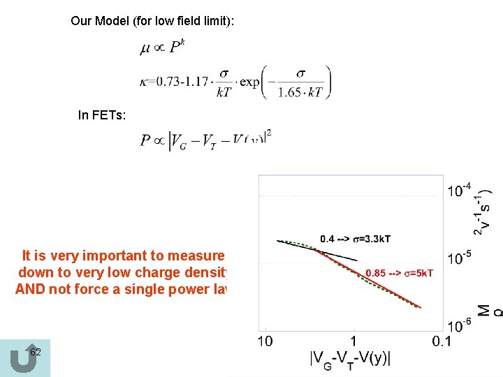
Our Model (for low field limit): In FETs: 84321 - It is very important to measure down to very low charge density AND 2 k=0. 85± 0. 1 not force a single power law 62 s≈5 k. T=130 me. V VDS

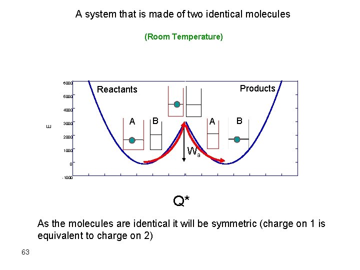
A system that is made of two identical molecules (Room Temperature) 6000 5000 Products Reactants E 4000 3000 A B 2000 1000 Wa 0 -1000 Q* As the molecules are identical it will be symmetric (charge on 1 is equivalent to charge on 2) 63

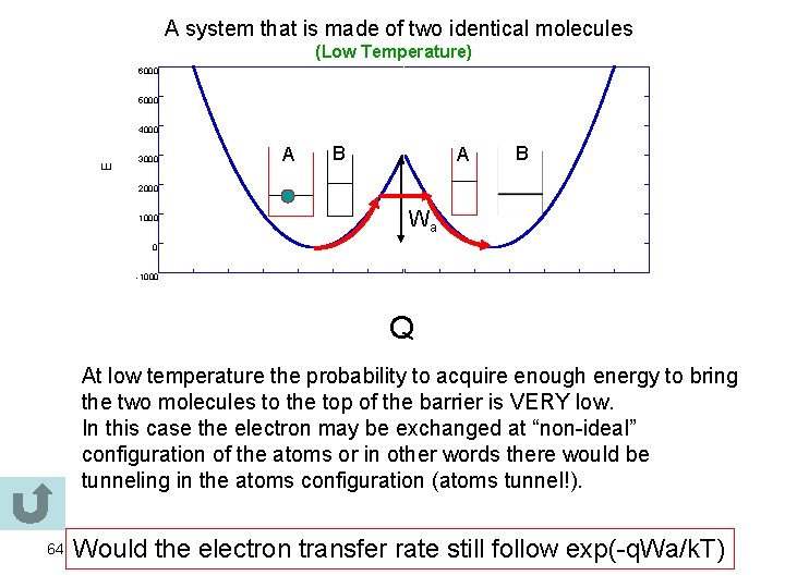
A system that is made of two identical molecules (Low Temperature) 6000 5000 E 4000 3000 A B 2000 1000 Wa 0 -1000 Q At low temperature the probability to acquire enough energy to bring the two molecules to the top of the barrier is VERY low. In this case the electron may be exchanged at “non-ideal” configuration of the atoms or in other words there would be tunneling in the atoms configuration (atoms tunnel!). 64 Would the electron transfer rate still follow exp(-q. Wa/k. T)

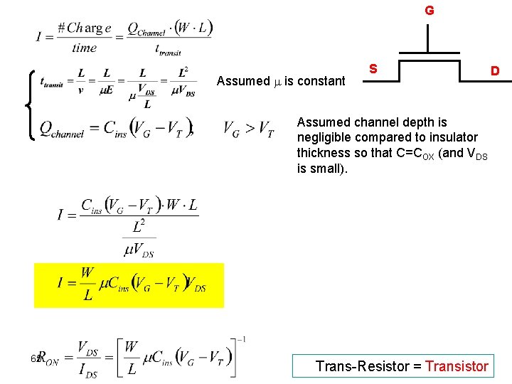
G Assumed m is constant S Assumed channel depth is negligible compared to insulator thickness so that C=COX (and VDS is small). 65 Trans-Resistor = Transistor D

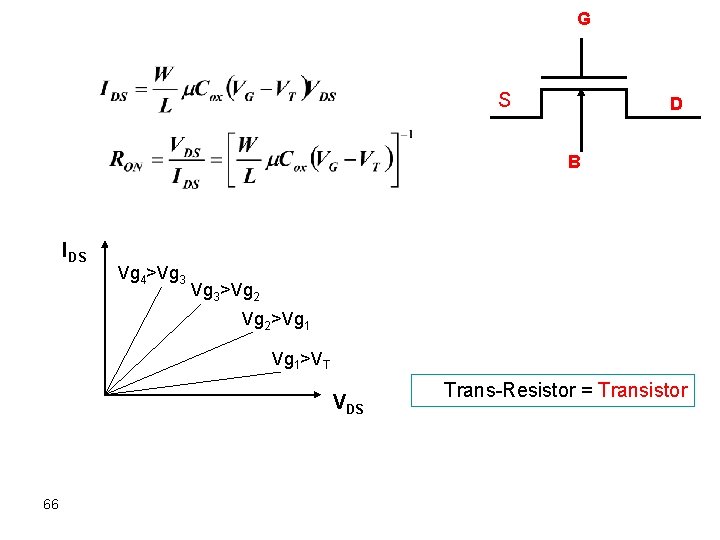
G S D B IDS Vg 4>Vg 3>Vg 2>Vg 1>VT VDS 66 Trans-Resistor = Transistor

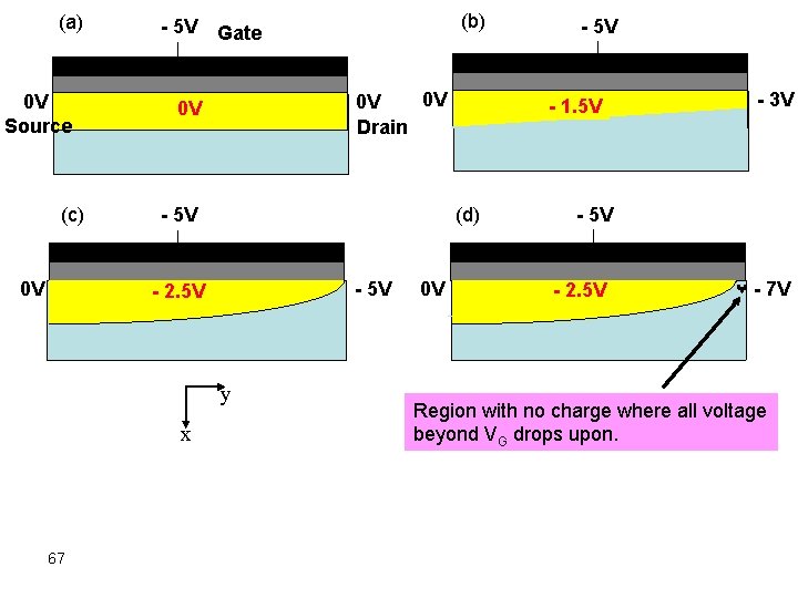
(a) 0 V Source (c) 0 V - 5 V 0 V 0 V Drain 0 V - 5 V y x 0 V - 5 V - 1. 5 V (d) - 2. 5 V 67 (b) Gate - 3 V - 5 V - 2. 5 V - 7 V Region with no charge where all voltage beyond VG drops upon.

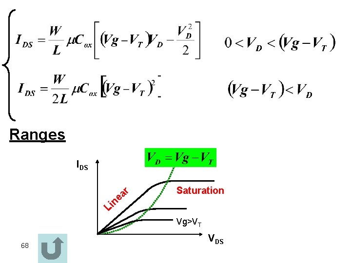
Ranges IDS r a e Saturation n Li Vg>VT 68 VDS