The Processor Data Path Control Chapter 5 Part
- Slides: 26

The Processor Data Path & Control Chapter 5 Part 2 - Multi-Clock Cycle Design N. Guydosh 2/29/04

A Multicycle Design • As pointed out earlier, a single clock cycle design has a performance bottleneck – namely the instruction requiring the longest time will determine the time for all other instructions even simple instructions such as jump (j). • The offending instruction is the load word memory instruction (lw) lw uses five functional units of in series: – – – Instruction memory (fetch) The register file (read) The ALU (compute address) Data memory (read) The register file (write) • Several instruction classes could fit into a shorter clock cycle, thus overall performance will be compromised – memory instructions may not be a frequently used instruction – but it determines timing for “simpler” instructions. • In addition single cycle increases hardware units – cannot multiplex in time. • See performance example on pp. 373 -375

Multiple Clock Cycle Design. . . Overview • Allows shorter clock cycle – Clock cycle derived from longest functional unit delay and not the longest total data path delay • • • Multiple clock pulses per instruction Use a clock pulse for each functional unit (memory, register file, alu, . . . ). . “multiplex” (share) in time not in space (as with single clock) Instead of a single long clock pulse, use a sequence of short pulses Average instruction time will be shorter - short instructions will not have to wait idle for the clock to time out. Another advantage: hardware is reduced. Instructions and data stored in same memory A single ALU will do all the arithmetic Time shared functional units. This approach is easily extended to pipelining which allows multiple instructions to executed at one time and which will further enhance performance (chapter 6).

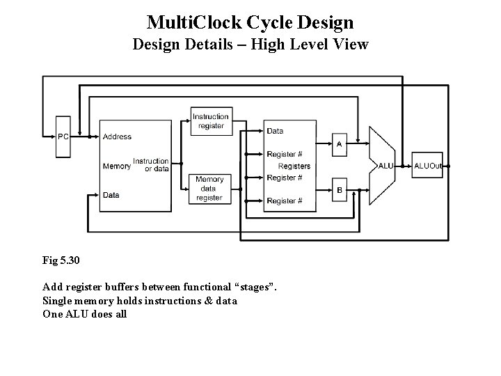
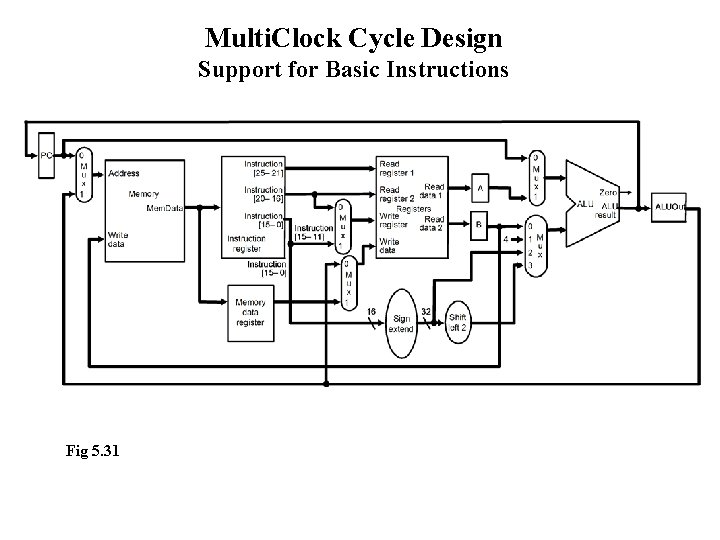
Multiple Clock Cycle Design Details • • We will use the single clock design as a starting point fig. 5. 29, p. 372) This design will be “compressed” into what you see in fig. 5. 30, p. 378. . . Single inst memory & one ALU for all (see next). – Single memory unit for both instructions and data – Single ALU instead of ALU and two adders – One or more “buffer” registers added after every major functional unit to hold output until next subsequent clock cycle. • Because functional units are now shared for various phases of execution, must add MUX’s and extend some existing MUX’s. See fig 5. 31, page 380 (see later). • A few additional hardware elements will also be added to resolve situations where stored data may change in one execution phase before a down stream phase gets to us it: – For now: we add an instruction register (IR) - this is to hold the instruction for later phases during execution after the PC is changed during the fetch stage and perhaps the memory get reused during execution.

Multi. Clock Cycle Design Details – High Level View Fig 5. 30 Add register buffers between functional “stages”. Single memory holds instructions & data One ALU does all

Multi. Clock Cycle Design Support for Basic Instructions Fig 5. 31

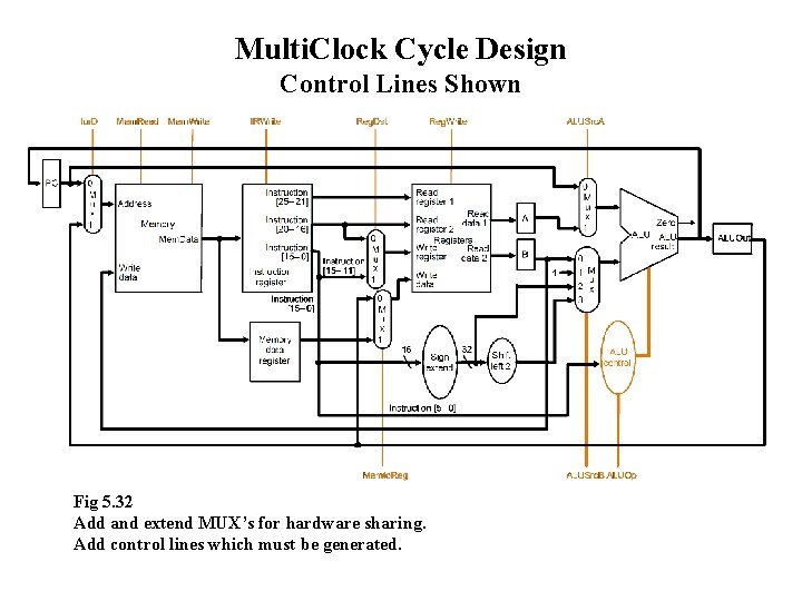
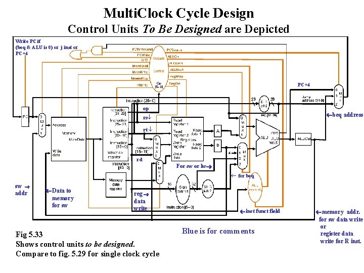
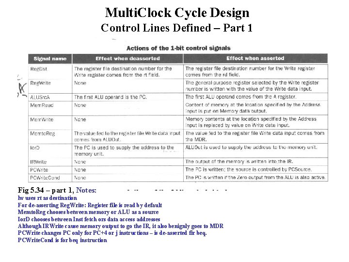
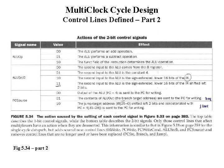
Multiple Clock Cycle Design Details (continued) • We will also need more control lines, and modify existing ones Control is now sequential and dynamic: – Time and opcode dependent – Things start to get hairy when we design the controller. . . But “Don’t Panic!” as Douglas Adams would say. • • The first cut at the data path design with control lines shown is fig 5. 32, page 381 All storage elements will need a separate write signal, and a read signal is needed for memory. The old ALU controller from single clock pulse will be reused. See fig 5. 34 p. 384 for a complete summary of the control line functions.

Multi. Clock Cycle Design Control Lines Shown Fig 5. 32 Add and extend MUX’s for hardware sharing. Add control lines which must be generated.

Multi. Clock Cycle Design Control Units To Be Designed are Depicted Write PC if (beq & ALU is 0) or j inst or PC+4 op beq address rs rt rd For sw or lw for beq sw addr Data to memory for sw reg data write Fig 5. 33 Shows control units to be designed. Compare to fig. 5. 29 for single clock cycle inst funct field Blue is for comments memory addr. for sw data write or register data write for R inst.

Multi. Clock Cycle Design Control Lines Defined – Part 1 Fig 5. 34 – part 1, Notes: lw uses rt as destination For de-asserting Reg. Write: Register file is read by default Memto. Reg chooses between memory or ALU as a source Ior. D chooses between Inst fetch ors data access addresses Although IRWrite cause memory output to go the IR, it also benignly goes to MDR PCWrite changes PC only for PC+4 or j instructions – is de-asserted fir beq. PCWrite. Cond is for beq instruction

Multi. Clock Cycle Design Control Lines Defined – Part 2 beq j inst Fig 5. 34 – part 2

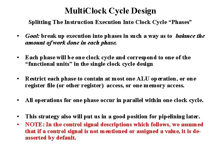
Multi. Clock Cycle Design Splitting The Instruction Execution Into Clock Cycle “Phases” • Goal: break up execution into phases in such a way as to balance the amount of work done in each phase. • Each phase will be one clock cycle and correspond to one of the “functional units” in the single clock cycle design • Restrict each phase to contain at most one ALU operation, or one register file (or other register) access, or one memory access. • All operations for one phase occur in parallel within one clock cycle. • This strategy also will put us in a good position for pipelining later. • NOTE: In the control signal descriptions which follows, we assumed that if a control signal is not mentioned or assigned a value, it is deasserted by default.

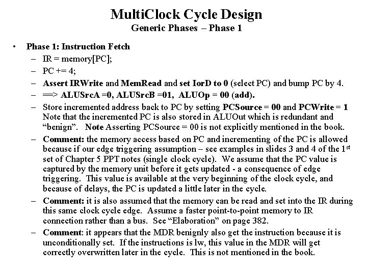
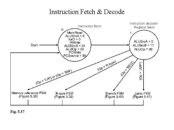
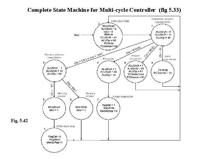
Multi. Clock Cycle Design Generic Phases – Phase 1 • Phase 1: Instruction Fetch – IR = memory[PC]; – PC += 4; – Assert IRWrite and Mem. Read and set Ior. D to 0 (select PC) and bump PC by 4. – ==> ALUSrc. A =0, ALUSrc. B =01, ALUOp = 00 (add). – Store incremented address back to PC by setting PCSource = 00 and PCWrite = 1 Note that the incremented PC is also stored in ALUOut which is redundant and “benign”. Note Asserting PCSource = 00 is not explicitly mentioned in the book. – Comment: the memory access based on PC and incrementing of the PC is allowed because if our edge triggering assumption – see examples in slides 3 and 4 of the 1 st set of Chapter 5 PPT notes (single clock cycle). We assume that the PC value is captured by the memory unit before it gets updated - a consequence of edge triggering. This value is available at the very beginning of the clock cycle, and because of delays, the PC is updated a little later in the cycle. – Comment: it is also assumed that the memory can be read and set into the IR during this same clock cycle edge. Assume a faster point-to-point memory to IR connection rather than a bus. See “Elaboration” on page 382. – Comment: it appears that the MDR benignly also get the instruction because it is unconditionally set. If the instructions is lw, this value in the MDR will get correctly overwritten later in the cycle. This is not mentioned in the book.

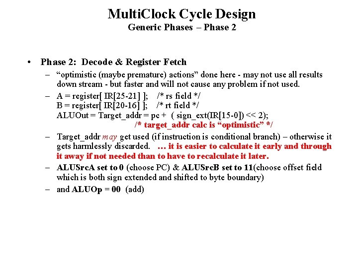
Multi. Clock Cycle Design Generic Phases – Phase 2 • Phase 2: Decode & Register Fetch – “optimistic (maybe premature) actions” done here - may not use all results down stream - but faster and will not cause any problem if not used. – A = register[ IR[25 -21] ]; /* rs field */ B = register[ IR[20 -16] ]; /* rt field */ ALUOut = Target_addr = pc + ( sign_ext(IR[15 -0]) << 2); /* target_addr calc is “optimistic” */ – Target_addr may get used (if instruction is conditional branch) – otherwise it gets harmlessly discarded. … it is easier to calculate it early and through it away if not needed than to have to recalculate it later. – ALUSrc. A set to 0 (choose PC) & ALUSrc. B set to 11(choose offset field which is both sign extended and shifted to byte boundary) – and ALUOp = 00 (add)

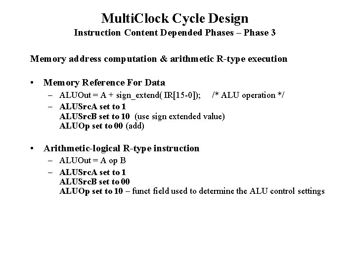
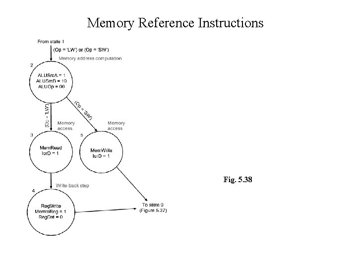
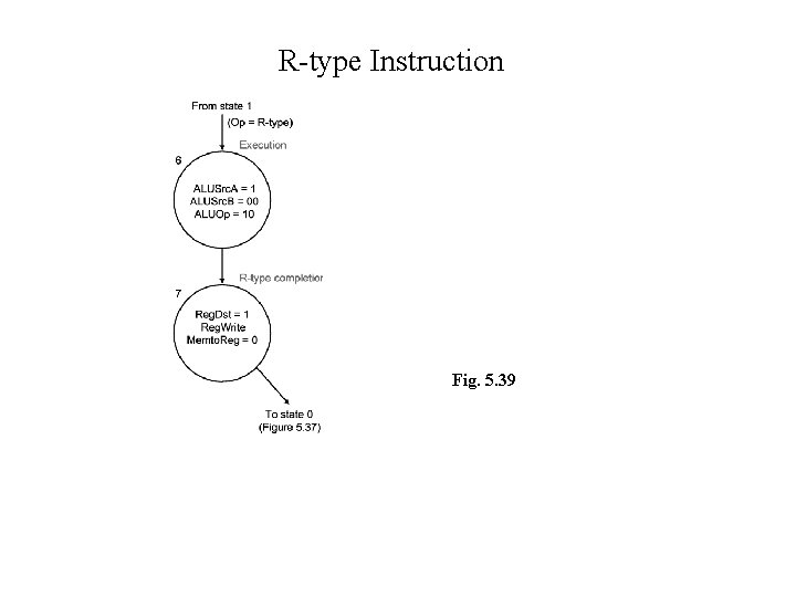
Multi. Clock Cycle Design Instruction Content Depended Phases – Phase 3 Memory address computation & arithmetic R-type execution • Memory Reference For Data – ALUOut = A + sign_extend( IR[15 -0]); /* ALU operation */ – ALUSrc. A set to 1 ALUSrc. B set to 10 (use sign extended value) ALUOp set to 00 (add) • Arithmetic-logical R-type instruction – ALUOut = A op B – ALUSrc. A set to 1 ALUSrc. B set to 00 ALUOp set to 10 – funct field used to determine the ALU control settings

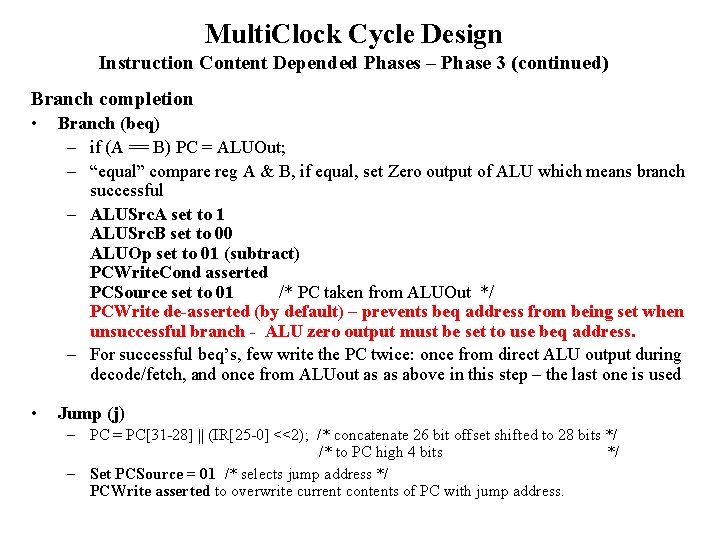
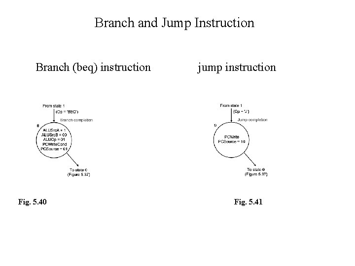
Multi. Clock Cycle Design Instruction Content Depended Phases – Phase 3 (continued) Branch completion • Branch (beq) – if (A == B) PC = ALUOut; – “equal” compare reg A & B, if equal, set Zero output of ALU which means branch successful – ALUSrc. A set to 1 ALUSrc. B set to 00 ALUOp set to 01 (subtract) PCWrite. Cond asserted PCSource set to 01 /* PC taken from ALUOut */ PCWrite de-asserted (by default) – prevents beq address from being set when unsuccessful branch - ALU zero output must be set to use beq address. – For successful beq’s, few write the PC twice: once from direct ALU output during decode/fetch, and once from ALUout as as above in this step – the last one is used • Jump (j) – PC = PC[31 -28] || (IR[25 -0] <<2); /* concatenate 26 bit offset shifted to 28 bits */ /* to PC high 4 bits */ – Set PCSource = 01 /* selects jump address */ PCWrite asserted to overwrite current contents of PC with jump address.

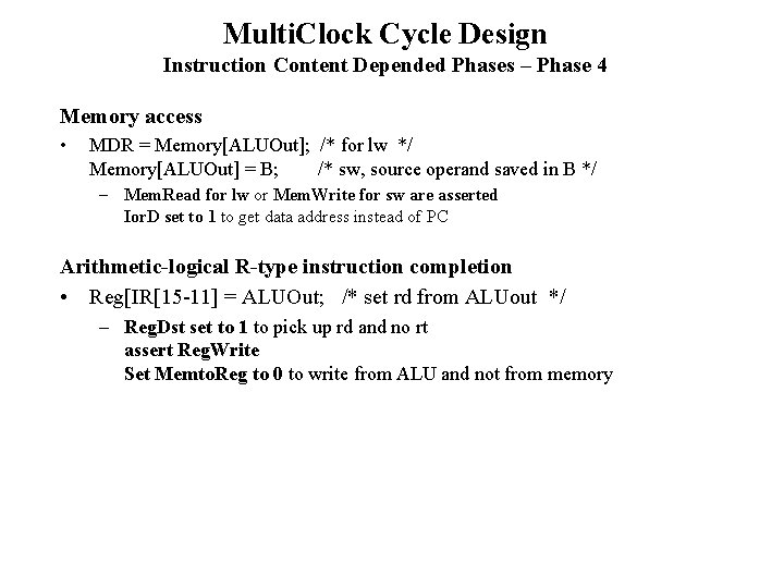
Multi. Clock Cycle Design Instruction Content Depended Phases – Phase 4 Memory access • MDR = Memory[ALUOut]; /* for lw */ Memory[ALUOut] = B; /* sw, source operand saved in B */ – Mem. Read for lw or Mem. Write for sw are asserted Ior. D set to 1 to get data address instead of PC Arithmetic-logical R-type instruction completion • Reg[IR[15 -11] = ALUOut; /* set rd from ALUout */ – Reg. Dst set to 1 to pick up rd and no rt assert Reg. Write Set Memto. Reg to 0 to write from ALU and not from memory

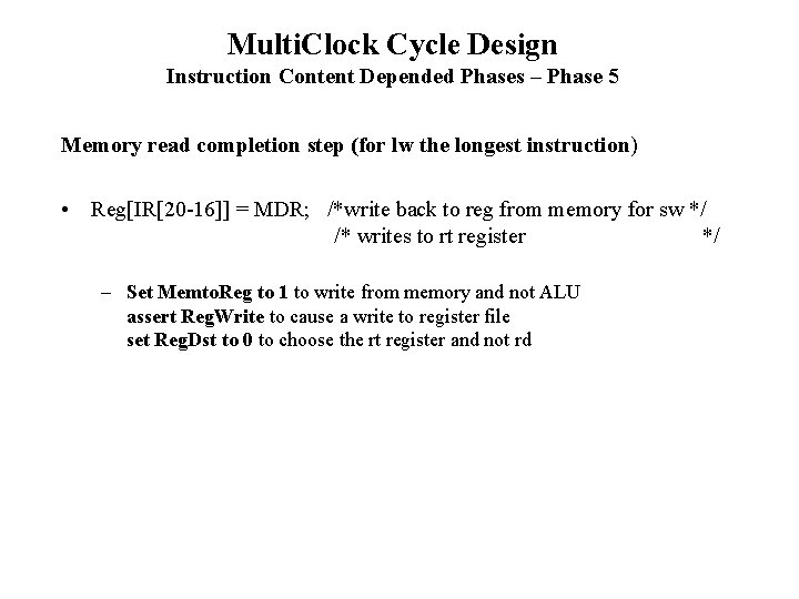
Multi. Clock Cycle Design Instruction Content Depended Phases – Phase 5 Memory read completion step (for lw the longest instruction) • Reg[IR[20 -16]] = MDR; /*write back to reg from memory for sw */ /* writes to rt register */ – Set Memto. Reg to 1 to write from memory and not ALU assert Reg. Write to cause a write to register file set Reg. Dst to 0 to choose the rt register and not rd

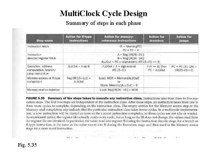
Multi. Clock Cycle Design Summary of steps in each phase Fig. 5. 35

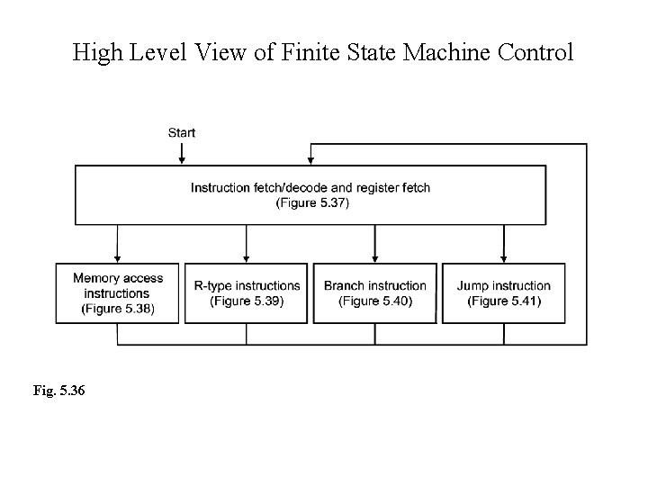
High Level View of Finite State Machine Control Fig. 5. 36

Instruction Fetch & Decode Fig. 5. 37

Memory Reference Instructions Fig. 5. 38

R-type Instruction Fig. 5. 39

Branch and Jump Instruction Branch (beq) instruction Fig. 5. 40 jump instruction Fig. 5. 41

Complete State Machine for Multi-cycle Controller (fig 5. 33) Fig. 5. 42

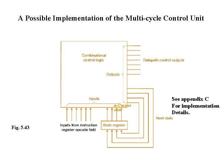
A Possible Implementation of the Multi-cycle Control Unit Current state Fig. 5. 43 See appendix C For implementation Details.