The Processor Data Path Control Chapter 5 Part
- Slides: 24

The Processor Data Path & Control Chapter 5 Part 1 - Introduction and Single Clock Cycle Design N. Guydosh 2/29/04

• Starting point: Introduction – The specification of the MIPS instruction set drives the design of the hardware. – Will restrict design to integer type instructions – Arithmetic element design from chapter 4. • Identify common functions to all instructions, and within instruction classes – easy to do in a RISC architecture • – Instruction fetch – Access one or more registers – Use ALU Asserted signals – a high or low level of a signal which implies a logically “true” condition … an “action” level. The text will only assert a logically high level, ie. , a “ 1”. • Clocking – – Assume “edge triggered” clocking (as opposed to level sensitive). A storage circuit or flip-flop stores a value on the clock transition edge. Model is flip-flops with combinational logic between them Propagation delay through combinations logic between storage elements determines clock cycle length. – Single clock cycle vs. multi-clock cycle design approach

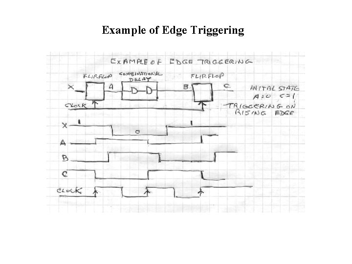
Example of Edge Triggering

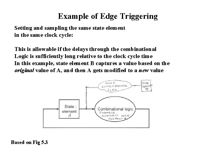
Example of Edge Triggering Setting and sampling the same state element in the same clock cycle: This is allowable if the delays through the combinational Logic is sufficiently long relative to the clock cycle time In this example, state element B captures a value based on the original value of A, and then A gets modified to a new value Based on Fig 5. 3

Single vs Multi-clock Cycle Design • Start out with a single “long” clock cycle for each instruction. – Entire instruction gets executed in a single clock pulse – Controller is pure combinational logic – Design is simple – You would think that a single clock cycle per instruction execution would give us super high performance – but not so: Slowest instruction determines speed of all instructions. – Ultimately we will go with a multi-clock cycle design – let each instruction run as fast is it could go – bottle neck is now not the slowest instruction, but the slowest “phase of execution” within an instruction – many instructions may never have this phase – penalize only those instructions employing the “slow phases” • Because various phases of the instructions need the same hardware resource, & all is needed at the same time (clock pulse) – Some hardware is redundant – another disadvantage of single phase Examples: 2 memories: instruction and data memory 2 adders and an ALU

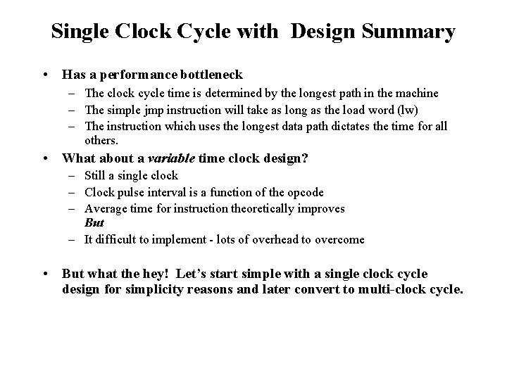
Single Clock Cycle with Design Summary • Has a performance bottleneck – The clock cycle time is determined by the longest path in the machine – The simple jmp instruction will take as long as the load word (lw) – The instruction which uses the longest data path dictates the time for all others. • What about a variable time clock design? – Still a single clock – Clock pulse interval is a function of the opcode – Average time for instruction theoretically improves But – It difficult to implement - lots of overhead to overcome • But what the hey! Let’s start simple with a single clock cycle design for simplicity reasons and later convert to multi-clock cycle.

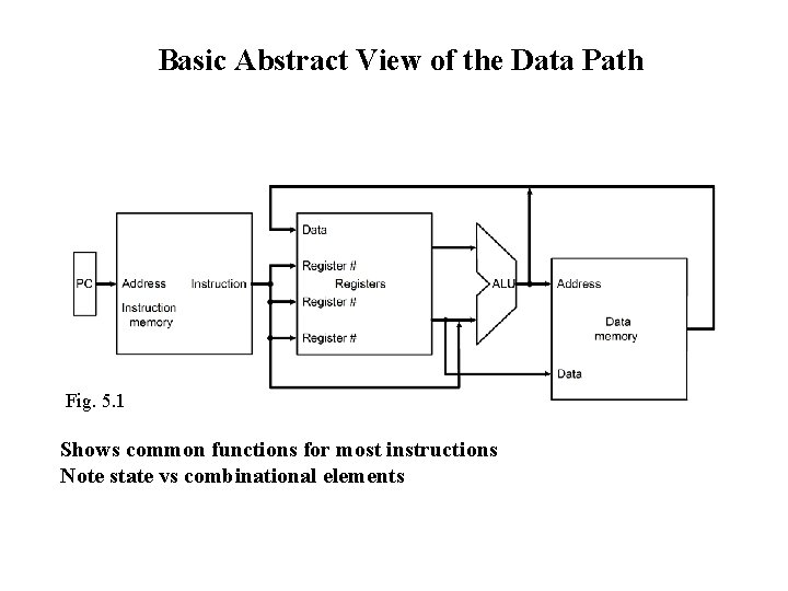
Basic Abstract View of the Data Path Fig. 5. 1 Shows common functions for most instructions Note state vs combinational elements

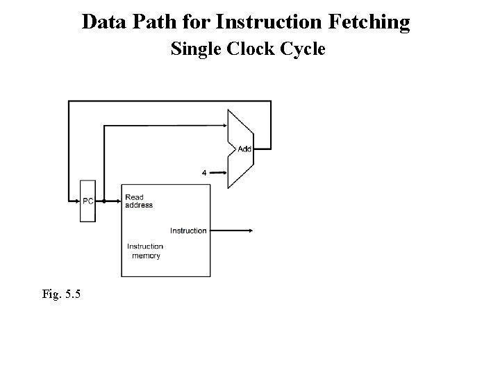
Data Path for Instruction Fetching Single Clock Cycle Fig. 5. 5

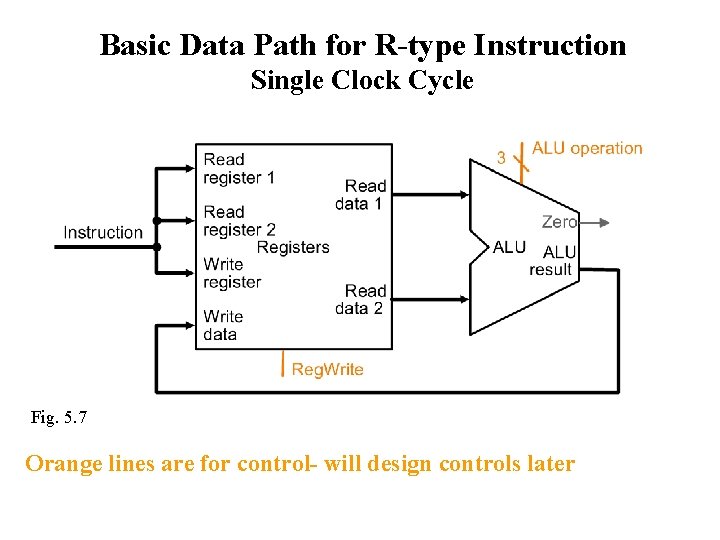
Basic Data Path for R-type Instruction Single Clock Cycle Fig. 5. 7 Orange lines are for control- will design controls later

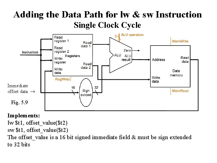
Adding the Data Path for lw & sw Instruction Single Clock Cycle Immediate offset data Fig. 5. 9 Implements: lw $t 1, offset_value($t 2) sw $t 1, offset_value($t 2) The offset_value is a 16 bit signed immediate field & must be sign extended to 32 bits

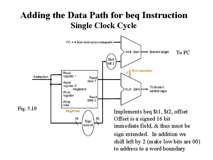
Adding the Data Path for beq Instruction Single Clock Cycle To PC Fig. 5. 10 Implements beq $t 1, $t 2, offset Offset is a signed 16 bit immediate field, & thus must be sign extended. In addition we shift left by 2 (make low bits are 00) to address to a word boundary

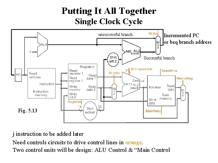
Putting It All Together Single Clock Cycle unsuccessful branch Incremented PC or beq branch address Successful branch Fig. 5. 13 j instruction to be added later Need controls circuits to drive control lines in orange. Two control units will be design: ALU Control & “Main Control

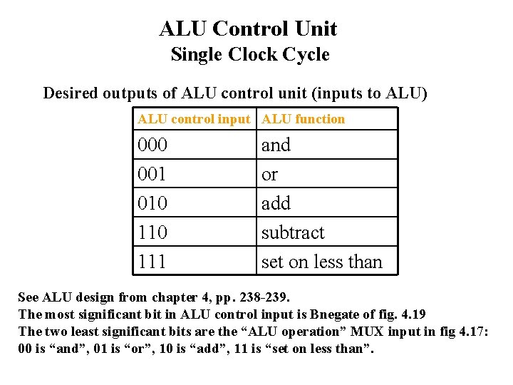
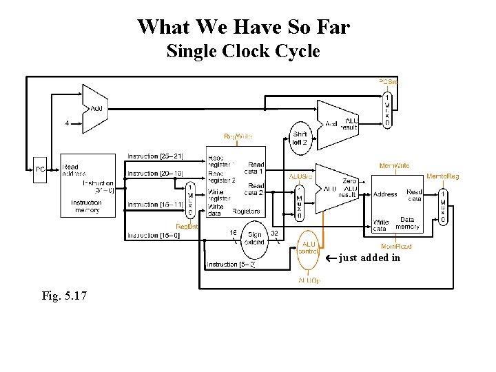
ALU Control Unit Single Clock Cycle Desired outputs of ALU control unit (inputs to ALU) ALU control input ALU function 000 001 010 111 and or add subtract set on less than See ALU design from chapter 4, pp. 238 -239. The most significant bit in ALU control input is Bnegate of fig. 4. 19 The two least significant bits are the “ALU operation” MUX input in fig 4. 17: 00 is “and”, 01 is “or”, 10 is “add”, 11 is “set on less than”.

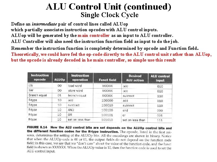
ALU Control Unit (continued) Single Clock Cycle Define an intermediate pair of control lines called ALUop which partially associates instruction opcodes with ALU control inputs. ALUop will be generated by the main controller as an input to ALU controller. ALU Controller will also need the instruction function field as input to do the job. Remember the instruction function is completely determined by opcode and Function field. Theoretically, we could have fed the op-code directly to the ALU control unit rather than ALUop, but the opcode is already decoded in he main controller, so simple use this result

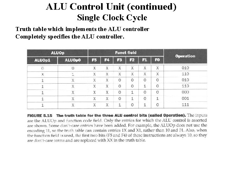
ALU Control Unit (continued) Single Clock Cycle Truth table which implements the ALU controller Completely specifies the ALU controller.

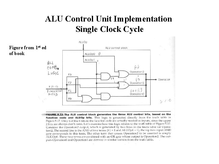
ALU Control Unit Implementation Single Clock Cycle Figure from 1 st ed of book

What We Have So Far Single Clock Cycle just added in Fig. 5. 17

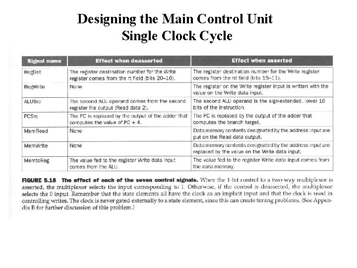
Designing the Main Control Unit Single Clock Cycle

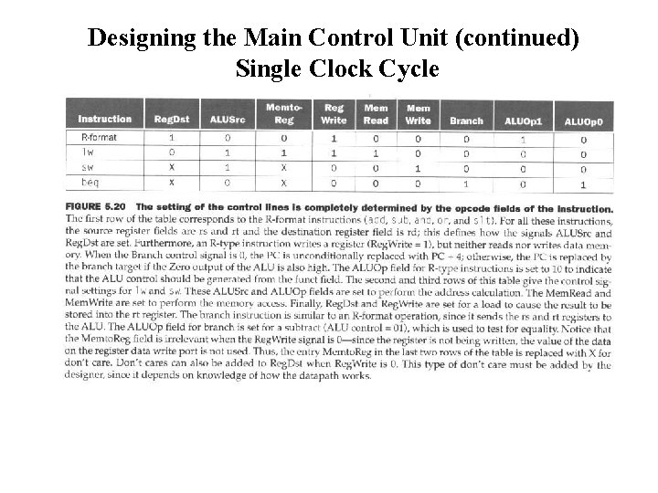
Designing the Main Control Unit (continued) Single Clock Cycle

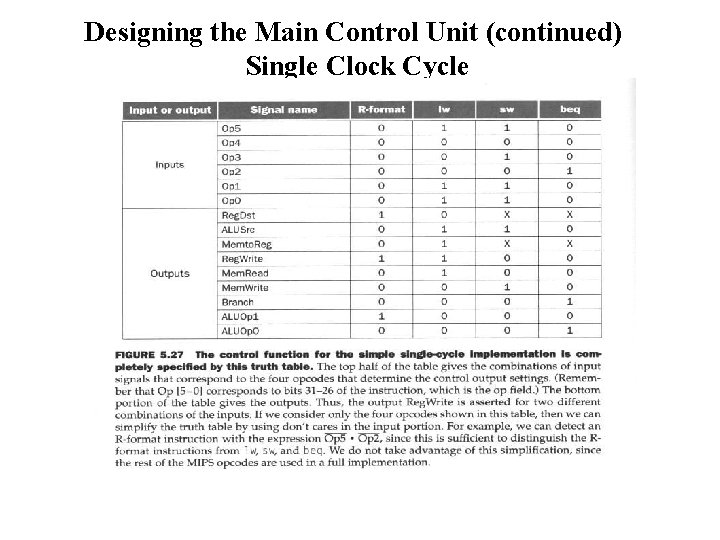
Designing the Main Control Unit (continued) Single Clock Cycle

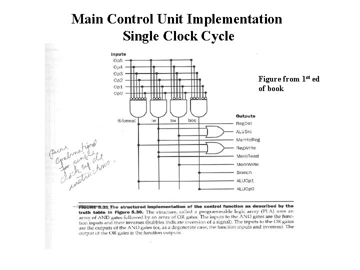
Main Control Unit Implementation Single Clock Cycle Figure from 1 st ed of book

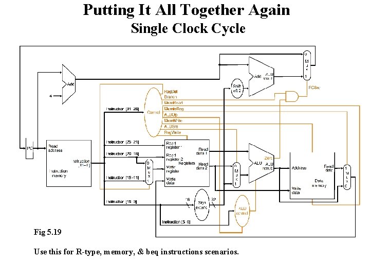
Putting It All Together Again Single Clock Cycle Fig 5. 19 Use this for R-type, memory, & beq instructions scenarios.

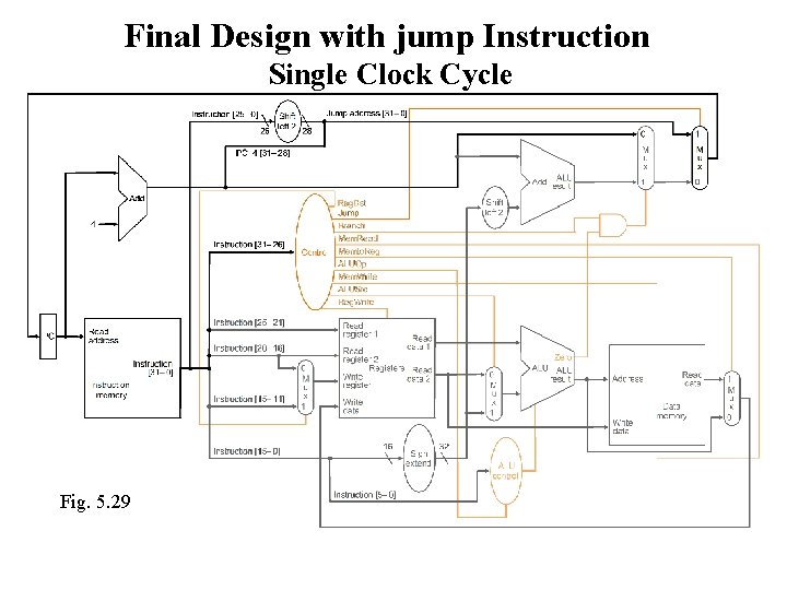
Addition of the Unconditional Jump Single Clock Cycle • We now add one more op code to our single cycle design: – Op code 2: “j” – The format is op field 28 -31 is a “ 2” – Remaining 26 low bits is the immediate target address • The full 32 bit target address is computed by concatenating: – – Upper 4 bits of PC+4 26 bit immediate field of the jump instruction Bits 00 in the lowest positions (word boundary) See text chapter 3, p. 150 • An additional control line from the main controller will have to be generated to select this “new” instruction • A two bit shifter is also added to get the two low order zeros

Final Design with jump Instruction Single Clock Cycle Fig. 5. 29