SUPERCONDUCTING THIN FILMS FOR SRF CAVITIES Stuart Wilde
- Slides: 23

SUPERCONDUCTING THIN FILMS FOR SRF CAVITIES Stuart Wilde STFC Daresbury Laboratory and Loughborough University Dr Reza Valizadeh and Dr Oleg Malyshev STFC Daresbury Laboratory Dr Boris Chesca Loughborough University

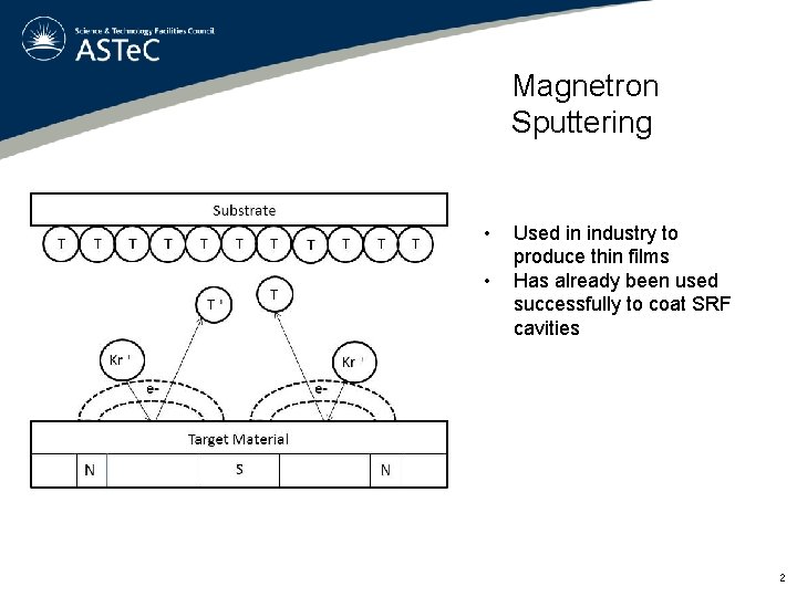
Magnetron Sputtering • • Used in industry to produce thin films Has already been used successfully to coat SRF cavities 2

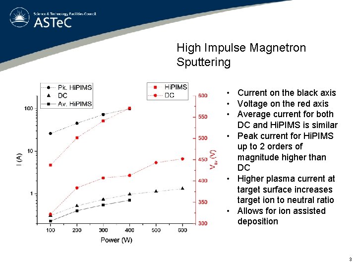
High Impulse Magnetron Sputtering • Current on the black axis • Voltage on the red axis • Average current for both DC and Hi. PIMS is similar • Peak current for Hi. PIMS up to 2 orders of magnitude higher than DC • Higher plasma current at target surface increases target ion to neutral ratio • Allows for ion assisted deposition 3

Experiment: To analyse the morphological and superconducting properties of Hi. PIMS films with changing temperature and / or DC substrate bias • Samples were deposited at room temperature, 500 °C, 700 °C and 800 °C • Films deposited with either a grounded substrate or substrate biased to -20, -50, -80, -100 and -120 V DC at each temperature • Films then analysed using XRD, SEM, EBSD, and DC SQUID magnetometry (support for XRD and DC SQUID provided by G. B. G. Stenning at STFC ISIS Laboratory) 4

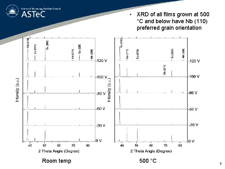
Hi. PIMS niobium on copper • Niobium thin films were deposited on polycrystalline Cu • Constant Hi. PIMS settings • Pulse width of 100 μs • Repetition rate of 200 Hz • Average current of 600 m. A • Peak current of 40 A • Kr sputter gas constant at 500 m. Torr 5

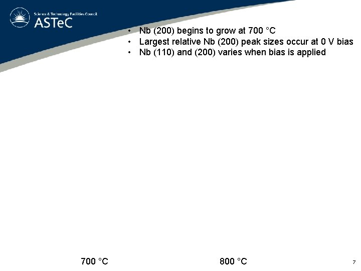
• XRD of all films grown at 500 °C and below have Nb (110) preferred grain orientation Room temp 500 °C 6

• Nb (200) begins to grow at 700 °C • Largest relative Nb (200) peak sizes occur at 0 V bias • Nb (110) and (200) varies when bias is applied 700 °C 800 °C 7

Lattice Constant • Lattice Constant was calculated to be longest for RT and 500 °C • Shorter lattice constants at highest temperatures 8

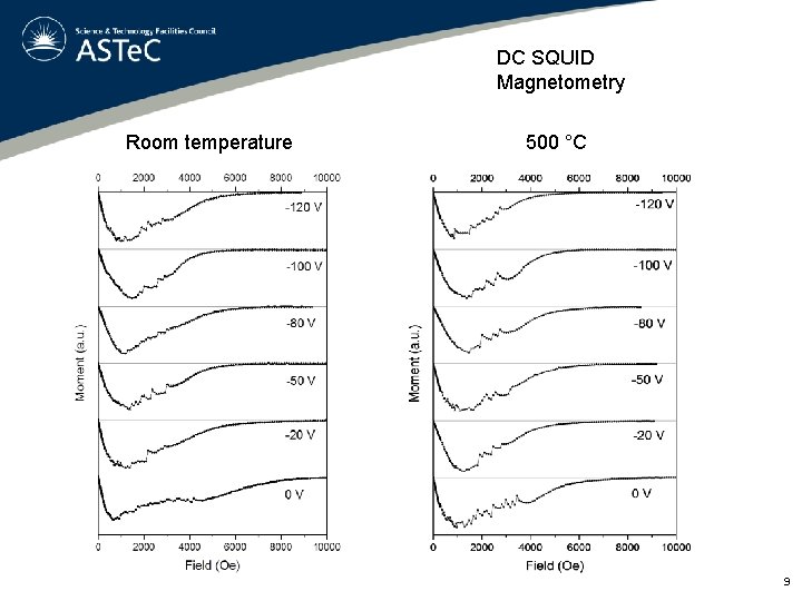
DC SQUID Magnetometry Room temperature 500 °C 9

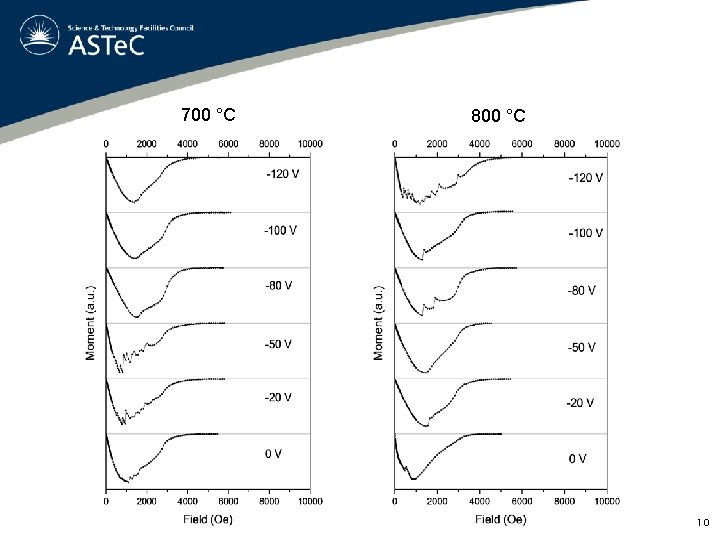
700 °C 800 °C 10

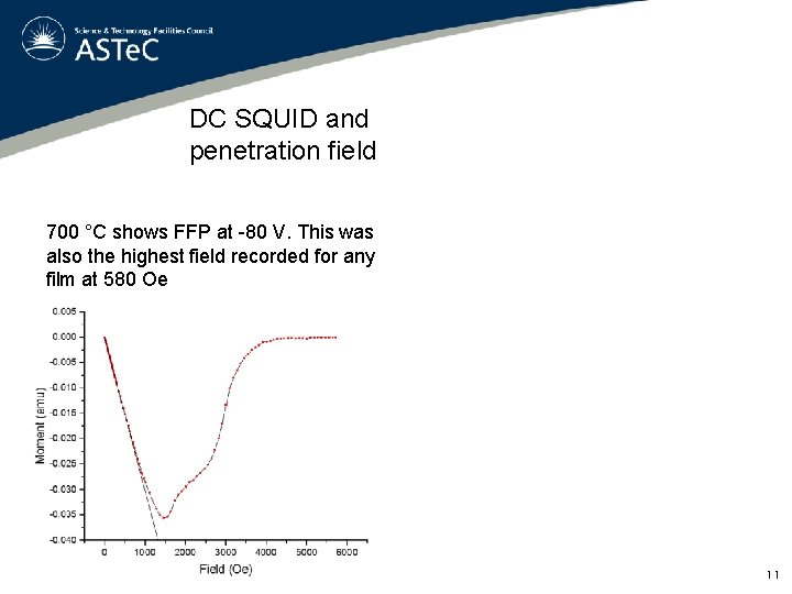
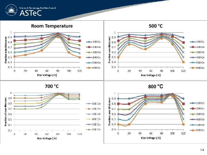
DC SQUID and penetration field 700 °C shows FFP at -80 V. This was also the highest field recorded for any film at 580 Oe 11

Summary showing peak at 80 / 100 V DC Bias 12

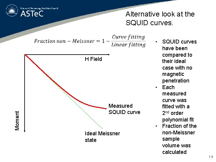
Alternative look at the SQUID curves. Moment H Field Measured SQUID curve Ideal Meissner state • SQUID curves have been compared to their ideal case with no magnetic penetration • Each measured curve was fitted with a 2 nd order polynomial fit • Fraction of the non-Meissner sample volume was calculated 13

14

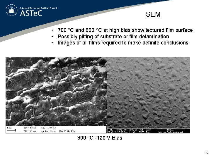
SEM • 700 °C and 800 °C at high bias show textured film surface • Possibly pitting of substrate or film delamination • Images of all films required to make definite conclusions 800 °C -120 V Bias 15

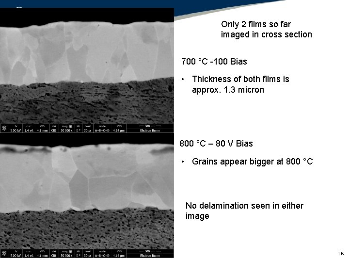
Only 2 films so far imaged in cross section 700 °C -100 Bias • Thickness of both films is approx. 1. 3 micron 800 °C – 80 V Bias • Grains appear bigger at 800 °C No delamination seen in either image 16

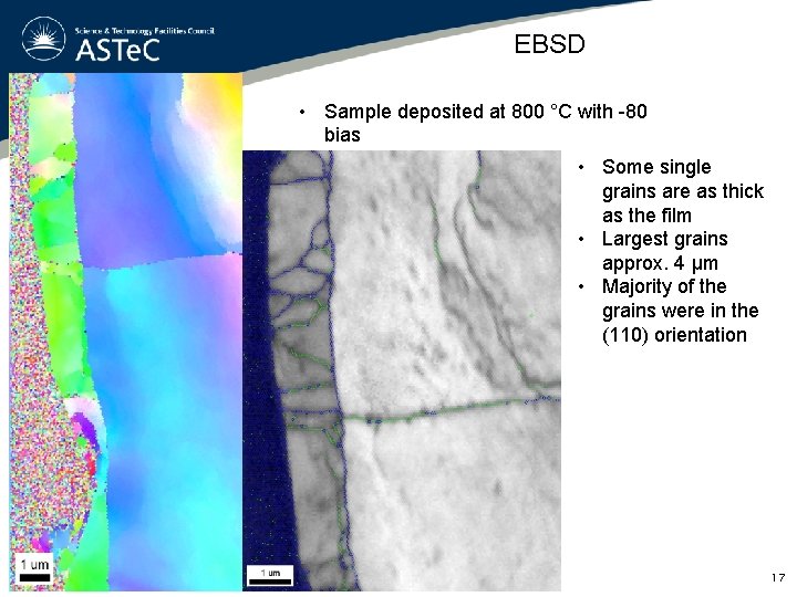
EBSD • Sample deposited at 800 °C with -80 bias • Some single grains are as thick as the film • Largest grains approx. 4 μm • Majority of the grains were in the (110) orientation 17

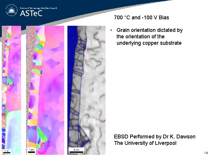
700 °C and -100 V Bias • Grain orientation dictated by the orientation of the underlying copper substrate EBSD Performed by Dr K. Dawson The University of Liverpool 18

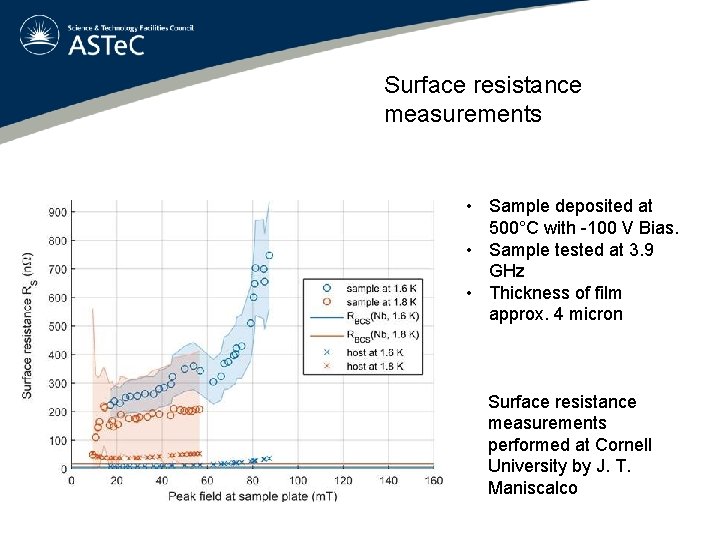
Surface resistance measurements • Sample deposited at 500°C with -100 V Bias. • Sample tested at 3. 9 GHz • Thickness of film approx. 4 micron Surface resistance measurements performed at Cornell University by J. T. Maniscalco

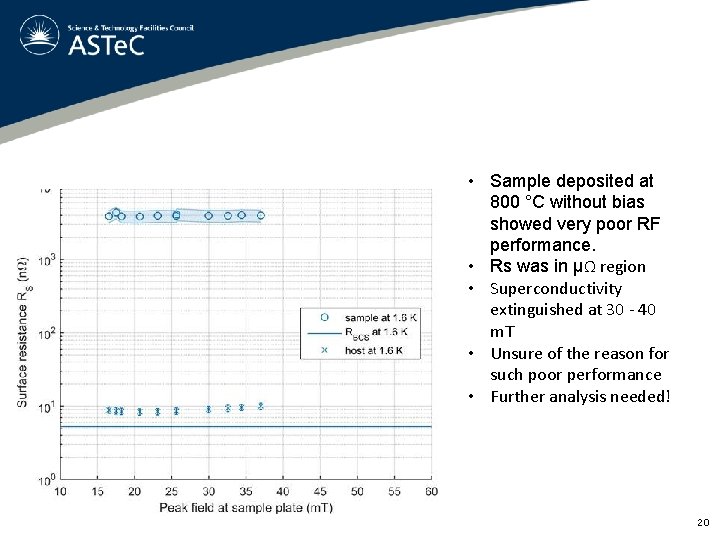
• Sample deposited at 800 °C without bias showed very poor RF performance. • Rs was in μΩ region • Superconductivity extinguished at 30 - 40 m. T • Unsure of the reason for such poor performance • Further analysis needed! 20

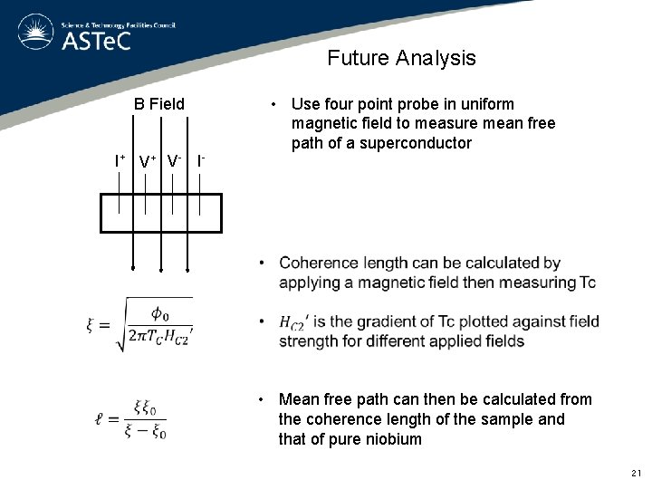
Future Analysis • Use four point probe in uniform magnetic field to measure mean free path of a superconductor B Field I+ V+ V- I- • Mean free path can then be calculated from the coherence length of the sample and that of pure niobium 21

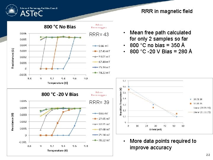
RRR in magnetic field Resistance (Ω) RRR= 43 • Mean free path calculated for only 2 samples so far • 800 °C no bias = 350 Å • 800 °C -20 V Bias = 280 Å RRR= 39 • More data points required to improve accuracy 22

Acknowledgments • • Reza Valizadeh Oleg Malyshev Gavin Stenning Shrikant Pattalwar Ninad Pattalwar Adrian Hannah Boris Chesca Karl Dawson 23