MATERIAL AND SURFACE ASPECTS IN SRF TECHNOLOGY SECOND
- Slides: 47
MATERIAL AND SURFACE ASPECTS IN SRF TECHNOLOGY SECOND PART : SURFACE CHEMISTRY Lectures on SRF 2018 C. Z. Antoine
ATOMIC DIFFUSION AT PLAY INTERACTION WITH SUBCRYSTALLINE STRUCTURE NON LOCAL TO LOCAL EFFECTS IN SC 2018 Lectures CZ. Antoine - Material & Surface Part II | PAGE 2
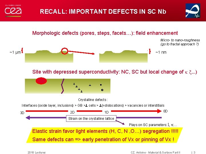
RECALL: IMPORTANT DEFECTS IN SC Nb Morphologic defects (pores, steps, facets…): field enhancement Micro- to nano-roughness (go to fractal approach ? ) ~1 nm ~1 µm Site with depressed superconductivity: NC, SC but local change of k x. . . ) . ° Crystalline defects : Interfaces (oxide layer, inclusions) > GB > cells > (=dislocations) > vacancies or interstitials 2 D 3 D 1 D 0 D Strain on the crystalline lattice Plays on SC parameters: l, k. . . Elastic strain favor light elements (H, C, N , O…) segregation !!!!! Same defects can => early penetration of Vx or pinning of Vx ! 2018 Lectures CZ. Antoine - Material & Surface Part II | 3
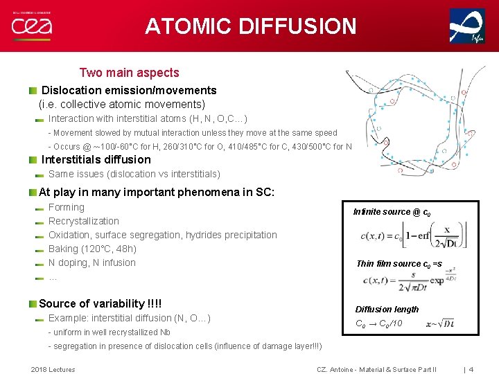
ATOMIC DIFFUSION Two main aspects Dislocation emission/movements (i. e. collective atomic movements) Interaction with interstitial atoms (H, N, O, C…) - - Movement slowed by mutual interaction unless they move at the same speed - - Occurs @ ~-100/-60°C for H, 260/310°C for O, 410/485°C for C, 430/500°C for N Interstitials diffusion Same issues (dislocation vs interstitials) At play in many important phenomena in SC: Forming Recrystallization Oxidation, surface segregation, hydrides precipitation Baking (120°C, 48 h) N doping, N infusion … Infinite source @ c 0 Thin film source c 0 =s Source of variability !!!! Diffusion length Example: interstitial diffusion (N, O…) C 0 → C 0 /10 - - uniform in well recrystallized Nb - - segregation in presence of dislocation cells (influence of damage layer!!!) 2018 Lectures CZ. Antoine - Material & Surface Part II | 4
SURFACE OXIDE : AN IMPORTANT 2 D DEFECT 2018 Lectures CZ. Antoine - Material & Surface Part II | PAGE 5
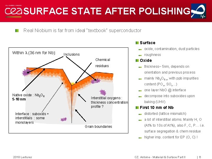
SURFACE STATE AFTER POLISHING Real Niobium is far from ideal “textbook” superconductor Surface Within l (36 nm for Nb): oxide, contamination, dust particles Inclusions roughness Chemical residues Oxide thickness~ 5 nm, depends on orientation and previous process mainly Nb 2 O 5 -x, with ppb impurities content (POx, SOx…) one layer Nb. O @ interface Native oxide : Nb 2 O 5 5 -10 nm Interstitial oxygens : thickness concentration profile ? decompose into suboxides upon baking (UHV) First 10 nm of Nb distorted (lattice mismatch) Interface : suboxids + interstitials : some monolayers a lot of interstitial atoms. Mainly H, O Grain boundaries (At% to 10 s of At%), also F, C, P… i. e. surface segregation & chem residue higher imp. content for EP (O, C) ! 2018 Lectures CZ. Antoine - Material & Surface Part II | 6
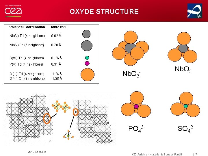
OXYDE STRUCTURE Valence/Coordination ionic radii Nb(V) Td (4 neighbors) 0. 62 Å Nb(V)Oh (6 neighbors) 0. 78 Å S(VI) Td (4 neighbors) 0. 26 Å P(V) Td (4 neighbors) 0. 31 Å O(-II) Td (4 neighbors) O(-II) Oh (8 neighbors) 1. 24 Å 1. 28 Å Nb. O 3 - PO 432018 Lectures Nb. O 2 SO 42 - CZ. Antoine - Material & Surface Part II | 7
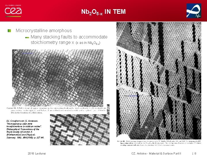
Nb 2 O 5 -x IN TEM Microcrystalline amorphous Many stacking faults to accommodate stoichiometry range x (x as in Nb 2 O 5 -x) E. S. Crawford and J. S. Anderson, "Homogeneous solid state transformations in niobium oxides". Philosophical Transactions of the Royal Society of London A (Mathematical-and-Physical. Sciences), 1982. 304(1485): p. 327 -64. 2018 Lectures CZ. Antoine - Material & Surface Part II | 8
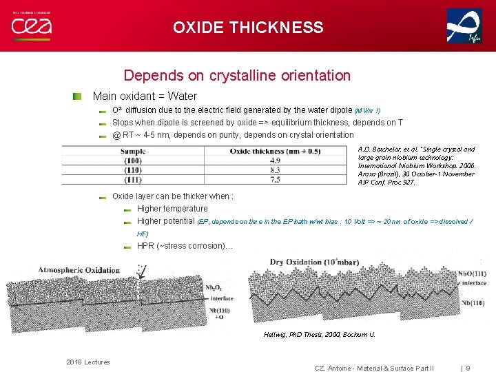
OXIDE THICKNESS Depends on crystalline orientation Main oxidant = Water O 2 - diffusion due to the electric field generated by the water dipole (MV/m !) Stops when dipole is screened by oxide => equilibrium thickness, depends on T @ RT ~ 4 -5 nm, depends on purity, depends on crystal orientation A. D. Batchelor, et al. "Single crystal and large grain niobium technology: International Niobium Workshop. 2006. Araxa (Brazil), 30 October-1 November AIP Conf. Proc 927. Oxide layer can be thicker when : Higher temperature Higher potential (EP, depends on time in the EP bath w/wt bias : 10 Volt => ~ 20 nm of oxide => dissolved / HF) HPR (~stress corrosion)… Diffusion barrier Hellwig, Ph. D Thesis, 2000, Bochum U. 2018 Lectures CZ. Antoine - Material & Surface Part II | 9
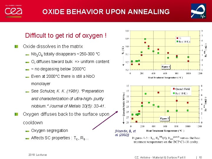
OXIDE BEHAVIOR UPON ANNEALING Difficult to get rid of oxygen ! Oxide dissolves in the matrix Nb 2 O 5 totally disappears ~250 -300 °C Oi diffuses toward bulk => uniform content ~ no degassing below 2000°C Even at 2000°C there is still a Nb. O monolayer See Schulze, K. K. (1981). "Preparation and characterization of ultra-high- purity niobium. " Journal of Metals 33(5): 33 -41. Oxygen diffuses back to the surface upon cooldown Oxygen segregation Affects SC properties : TC, RS… 2018 Lectures [Visentin, B. , et al. (2002)] CZ. Antoine - Material & Surface Part II | 10
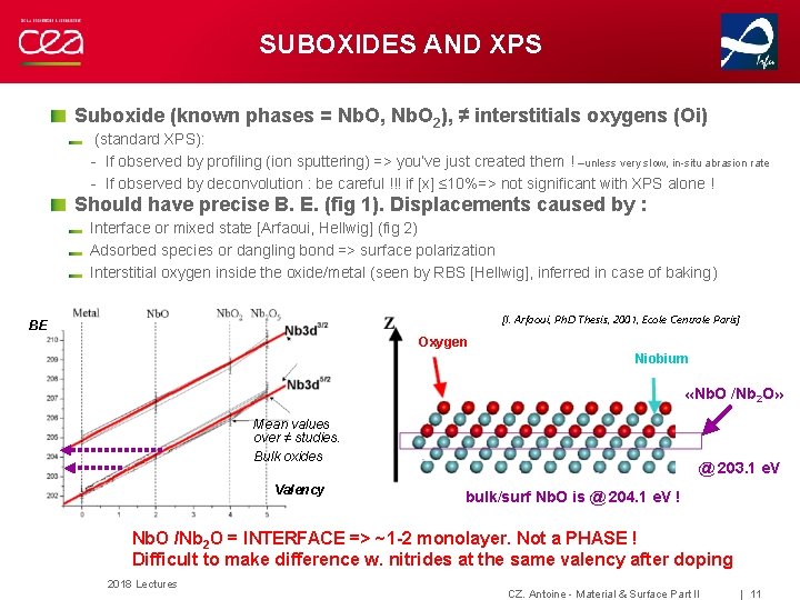
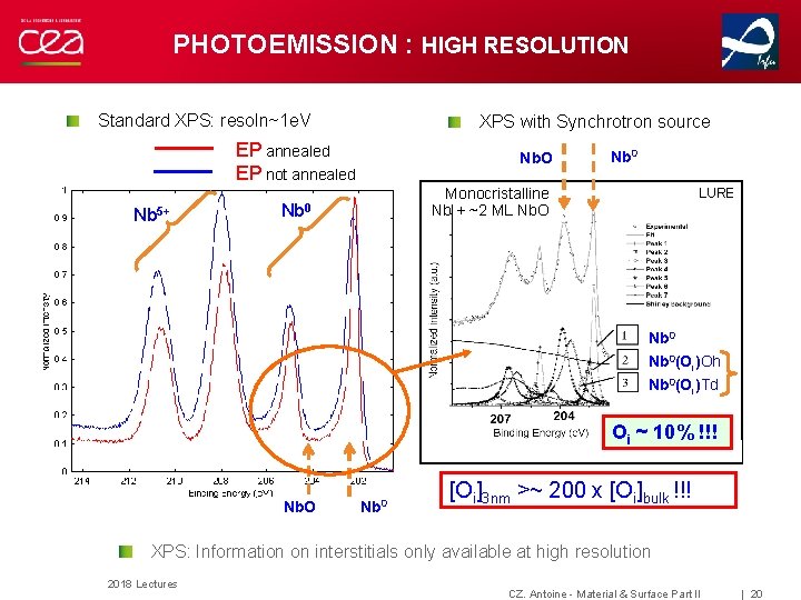
SUBOXIDES AND XPS Suboxide (known phases = Nb. O, Nb. O 2), ≠ interstitials oxygens (Oi) (standard XPS): - If observed by profiling (ion sputtering) => you’ve just created them ! –unless very slow, in-situ abrasion rate - If observed by deconvolution : be careful !!! if [x] ≤ 10%=> not significant with XPS alone ! Should have precise B. E. (fig 1). Displacements caused by : Interface or mixed state [Arfaoui, Hellwig] (fig 2) Adsorbed species or dangling bond => surface polarization Interstitial oxygen inside the oxide/metal (seen by RBS [Hellwig], inferred in case of baking) [I. Arfaoui, Ph. D Thesis, 2001, Ecole Centrale Paris] BE Oxygen Niobium «Nb. O /Nb 2 O» Mean values over ≠ studies. Bulk oxides Valency @ 203. 1 e. V bulk/surf Nb. O is @ 204. 1 e. V ! Nb. O /Nb 2 O = INTERFACE => ~1 -2 monolayer. Not a PHASE ! Difficult to make difference w. nitrides at the same valency after doping 2018 Lectures CZ. Antoine - Material & Surface Part II | 11
SURFACE SEGREGATION 2018 Lectures CZ. Antoine - Material & Surface Part II | PAGE 12
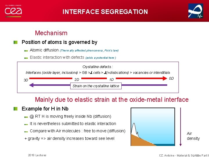
INTERFACE SEGREGATION Mechanism Position of atoms is governed by Atomic diffusion (Thermally affected phenomena, Fick’s law) Elastic interaction with defects (adds a potential term) Crystalline defects : Interfaces (oxide layer, inclusions) > GB > cells > (=dislocations) > vacancies or interstitials 2 D 3 D 1 D 0 D Strain on the crystalline lattice Mainly due to elastic strain at the oxide-metal interface Example for H in Nb @ RT H is moving freely inside Nb (diffusion) It is nevertheless submitted to elastic interaction Compare with Air molecules : free to move (diffusion) + gravity => air density increases toward see level 2018 Lectures Air density | 13 CZ. Antoine - Material & Surface Part II
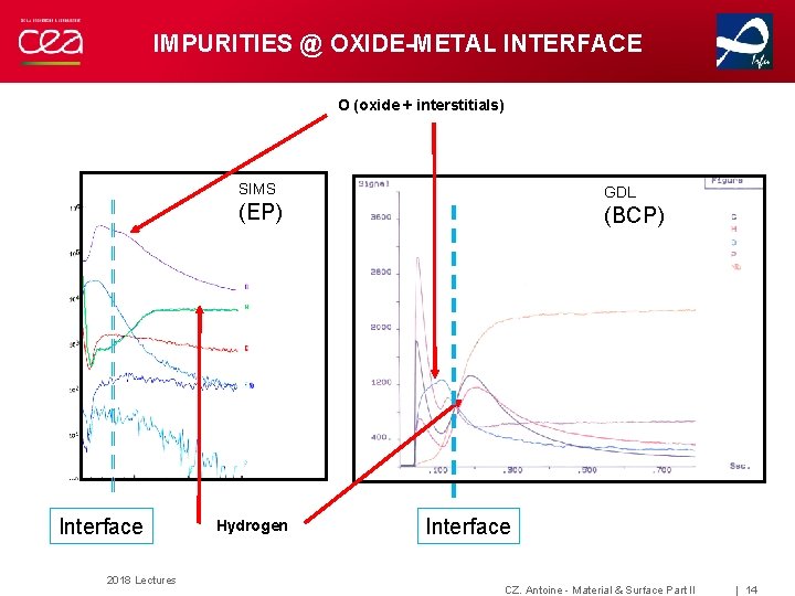
IMPURITIES @ OXIDE-METAL INTERFACE O (oxide + interstitials) SIMS GDL (EP) (BCP) H Interface 2018 Lectures Hydrogen Interface CZ. Antoine - Material & Surface Part II | 14
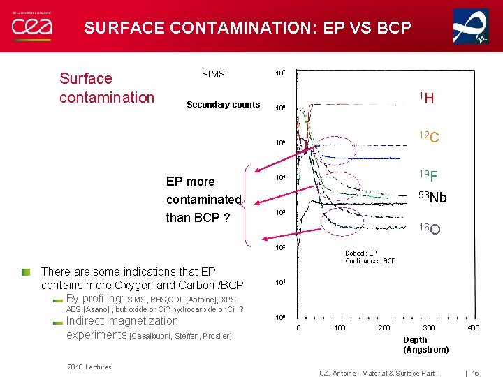
SURFACE CONTAMINATION: EP VS BCP Surface contamination SIMS Secondary counts EP more contaminated than BCP ? 107 1 H 106 105 12 C 104 19 F 93 Nb 103 16 O 102 There are some indications that EP contains more Oxygen and Carbon /BCP By profiling: SIMS, RBS, GDL [Antoine], XPS, AES [Asano] , but oxide or Oi? hydrocarbide or Ci ? Indirect: magnetization experiments [Casalbuoni, Steffen, Proslier] 2018 Lectures 101 100 0 100 200 300 400 Depth (Angstrom) CZ. Antoine - Material & Surface Part II | 15
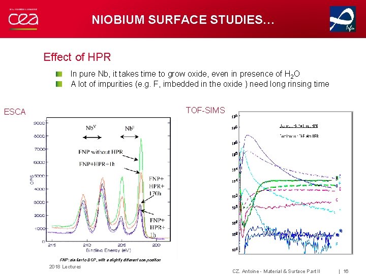
NIOBIUM SURFACE STUDIES… Effect of HPR In pure Nb, it takes time to grow oxide, even in presence of H 2 O A lot of impurities (e. g. F, imbedded in the oxide ) need long rinsing time TOF-SIMS ESCA FNP: similar to BCP, with a slightly different composition 2018 Lectures CZ. Antoine - Material & Surface Part II | 16
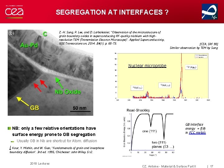
SEGREGATION AT INTERFACES ? Z. -H. Sung, P. Lee, and D. Larbalestier, "Observation of the microstructure of grain boundary oxides in superconducting RF-quality niobium with highresolution TEM (Transmission Electron Microscope)". Applied Superconductivity, IEEE Transactions on, 2014. 24(1): p. 68 -73. [CZA, SRF 98] Similar observation by TEM by Sung Nuclear microprobe NB: only a few relative orientations have surface energy prone to GB segregation GB Interface energy = f(q) in FCC metals Usually GB in Nb are shortcut for Atom. diffusion I. Kaur, Y. Mishin, and W. Gust, "Fundamentals of grain and interphase boundary diffusion". 3 rd ed. 1995, Chichester: John Wiley. 512. 2018 Lectures CZ. Antoine - Material & Surface Part II | 17
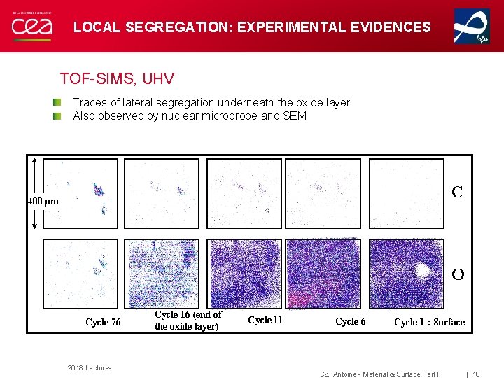
LOCAL SEGREGATION: EXPERIMENTAL EVIDENCES TOF-SIMS, UHV Traces of lateral segregation underneath the oxide layer Also observed by nuclear microprobe and SEM C 400 µm O Cycle 76 2018 Lectures Cycle 16 (end of the oxide layer) Cycle 11 Cycle 6 Cycle 1 : Surface CZ. Antoine - Material & Surface Part II | 18
INTERSTITIAL OXYGEN AND BAKING • • 2018 Lectures O = MAIN IMPURITY IN Nb O = MODEL FOR N OR C BEHAVIOR IN Nb (SEE § ON DOPING) CZ. Antoine - Material & Surface Part II | PAGE 19
PHOTOEMISSION : HIGH RESOLUTION Standard XPS: resoln~1 e. V XPS with Synchrotron source EP annealed EP not annealed Nb 5+ Nb. O Nb 0 Monocristalline Nb + ~2 ML Nb. O Nb 0 LURE Nb 0(Oi)Oh Nb 0(Oi)Td Oi ~ 10% !!! Nb. O Nb 0 [Oi]3 nm >~ 200 x [Oi]bulk !!! XPS: Information on interstitials only available at high resolution 2018 Lectures CZ. Antoine - Material & Surface Part II | 20
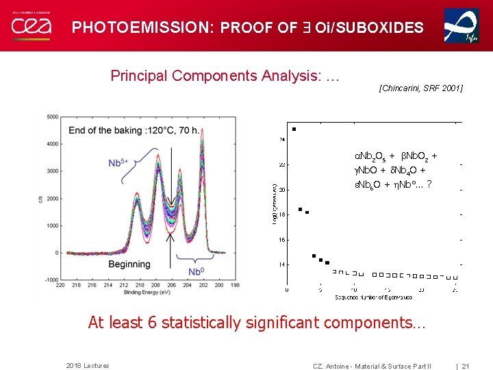
PHOTOEMISSION: PROOF OF Oi/SUBOXIDES Principal Components Analysis: … [Chincarini, SRF 2001] a. Nb 2 O 5 + b. Nb. O 2 + g. Nb. O + d. Nb 4 O + e. Nb 6 O + h. Nb°… ? At least 6 statistically significant components… 2018 Lectures CZ. Antoine - Material & Surface Part II | 21
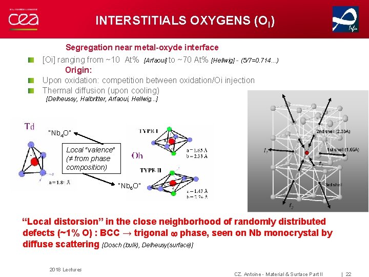
INTERSTITIALS OXYGENS (OI) Segregation near metal-oxyde interface [Oi] ranging from ~10 At% [Arfaoui] to ~70 At% [Hellwig] - (5/7=0. 714…) Origin: Upon oxidation: competition between oxidation/Oi injection Thermal diffusion (upon cooling) [Delheussy, Halbritter, Arfaoui, Hellwig. . . ] “Nb 4 O” Local “valence” (≠ from phase composition) “Nb 6 O” “Local distorsion” in the close neighborhood of randomly distributed defects (~1% O) : BCC → trigonal w phase, seen on Nb monocrystal by diffuse scattering [Dosch (bulk), Delheusy(surface)] 2018 Lectures CZ. Antoine - Material & Surface Part II | 22
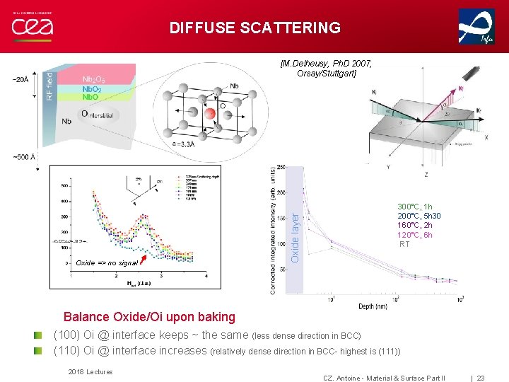
DIFFUSE SCATTERING Oxide => no signal Oxide layer [M. Delheusy, Ph. D 2007, Orsay/Stuttgart] 300°C, 1 h 200°C, 5 h 30 160°C, 2 h 120°C, 6 h RT Balance Oxide/Oi upon baking (100) Oi @ interface keeps ~ the same (less dense direction in BCC) (110) Oi @ interface increases (relatively dense direction in BCC- highest is (111)) 2018 Lectures CZ. Antoine - Material & Surface Part II | 23
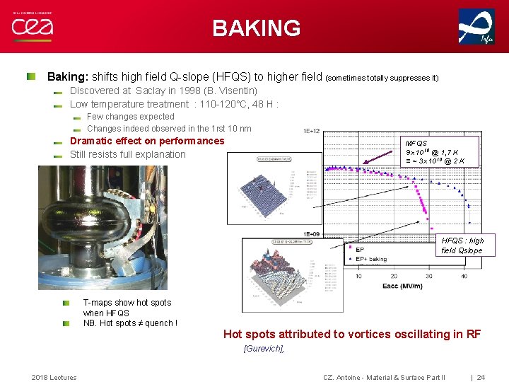
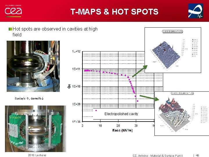
BAKING Baking: shifts high field Q-slope (HFQS) to higher field (sometimes totally suppresses it) Discovered at Saclay in 1998 (B. Visentin) Low temperature treatment : 110 -120°C, 48 H : Few changes expected Changes indeed observed in the 1 rst 10 nm Dramatic effect on performances Still resists full explanation MFQS 9 x 10¹⁰ @ 1, 7 K ≡ ~ 3 x 10¹⁰ @ 2 K HFQS : high field Qslope T-maps show hot spots when HFQS NB. Hot spots ≠ quench ! Hot spots attributed to vortices oscillating in RF [Gurevich], 2018 Lectures CZ. Antoine - Material & Surface Part II | 24
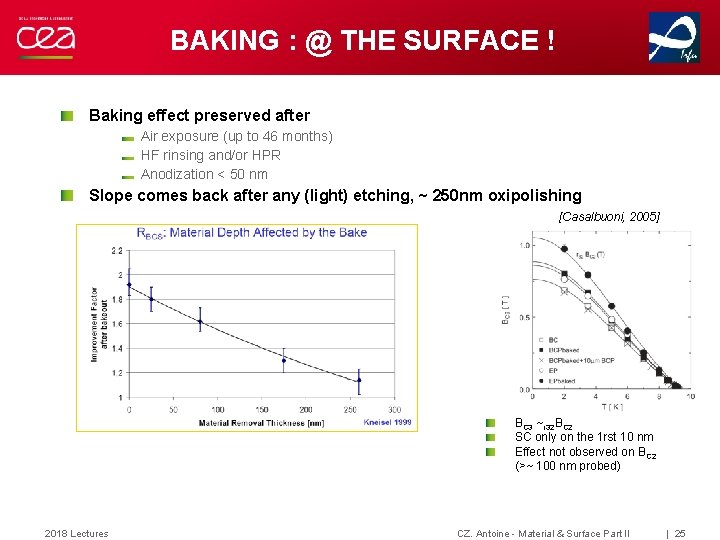
BAKING : @ THE SURFACE ! Baking effect preserved after Air exposure (up to 46 months) HF rinsing and/or HPR Anodization < 50 nm Slope comes back after any (light) etching, ~ 250 nm oxipolishing [Casalbuoni, 2005] BC 3 ~r 32 BC 2 SC only on the 1 rst 10 nm Effect not observed on BC 2 (>~ 100 nm probed) 2018 Lectures CZ. Antoine - Material & Surface Part II | 25
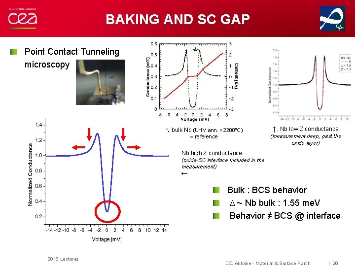
BAKING AND SC GAP Point Contact Tunneling microscopy ↑. bulk Nb (UHV ann. >2200°C) = reference ↑. Nb low Z conductance (measurement deep, past the oxide layer) Nb high Z conductance (oxide-SC interface included in the measurement) ← Bulk : BCS behavior D ~ Nb bulk : 1. 55 me. V Behavior ≠ BCS @ interface 2018 Lectures CZ. Antoine - Material & Surface Part II | 26
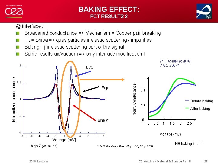
BAKING EFFECT: PCT RESULTS 2 @ interface : Broadened conductance => Mechanism = Cooper pair breaking Fit = Shiba => quasiparticles inelastic scattering / impurities Baking : ↓ inelastic scattering part of the signal Same results air/vacuum => only interface modification ! [T. Proslier et al, IIT, ANL, 2007] Exp Shiba* Norm. Conductance BCS 0. 1 _ Before baking _ After baking 0. 5 0 0 0. 5 1 1. 5 2 2. 5 Voltage (m. V) high Z (w. oxide) 2018 Lectures * H. Shiba Prog. Theo. Phys. 50, 50 (1973); NB baking in air ! CZ. Antoine - Material & Surface Part II | 27
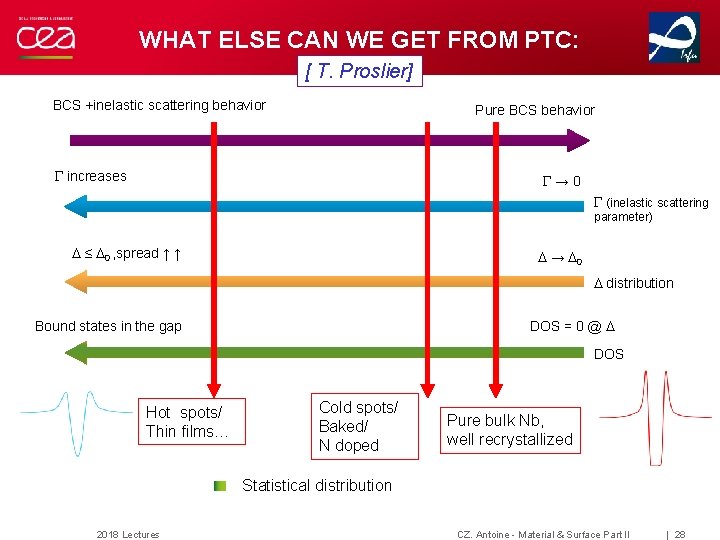
WHAT ELSE CAN WE GET FROM PTC: [ T. Proslier] BCS +inelastic scattering behavior Pure BCS behavior G increases G → 0 G (inelastic scattering parameter) D ≤ D 0 , spread ↑ ↑ D → D 0 D distribution Bound states in the gap DOS = 0 @ D DOS Hot spots/ Thin films… Cold spots/ Baked/ N doped Pure bulk Nb, well recrystallized Statistical distribution 2018 Lectures CZ. Antoine - Material & Surface Part II | 28
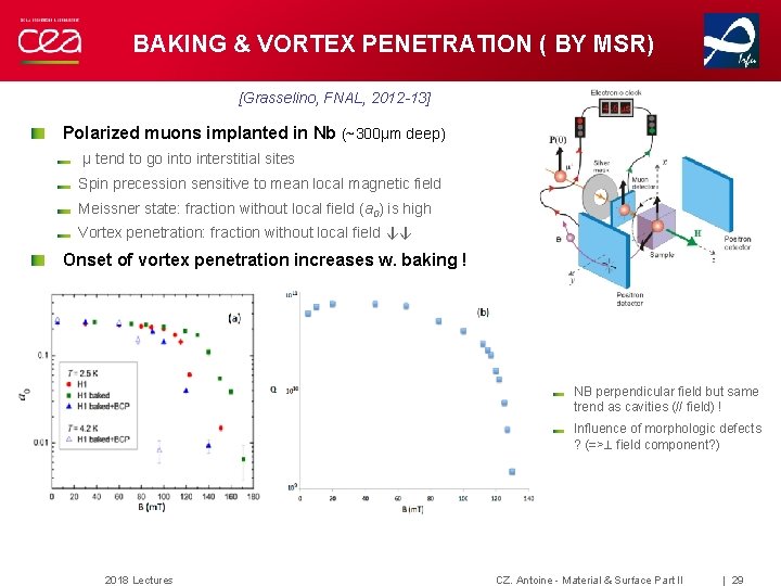
BAKING & VORTEX PENETRATION ( BY ΜSR) [Grasselino, FNAL, 2012 -13] Polarized muons implanted in Nb (~300µm deep) µ tend to go interstitial sites Spin precession sensitive to mean local magnetic field Meissner state: fraction without local field (a 0) is high Vortex penetration: fraction without local field ↓↓ Onset of vortex penetration increases w. baking ! NB perpendicular field but same trend as cavities (// field) ! Influence of morphologic defects ? (=> field component? ) 2018 Lectures CZ. Antoine - Material & Surface Part II | 29
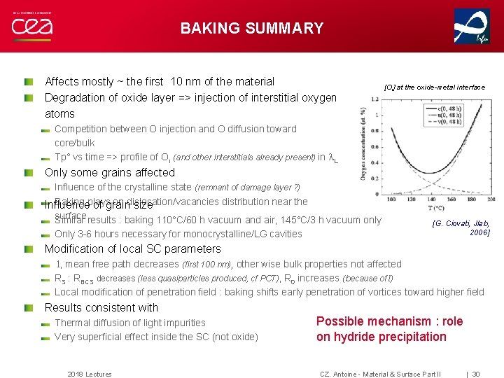
BAKING SUMMARY Affects mostly ~ the first 10 nm of the material Degradation of oxide layer => injection of interstitial oxygen atoms [Oi] at the oxide-metal interface Competition between O injection and O diffusion toward core/bulk Tp° vs time => profile of Oi (and other interstitials already present) in l. L Only some grains affected Influence of the crystalline state (remnant of damage layer ? ) Baking plays on dislocation/vacancies distribution near the Influence of grain size surface Similar results : baking 110°C/60 h vacuum and air, 145°C/3 h vacuum only Only 3 -6 hours necessary for monocrystalline/LG cavities [G. Ciovati, Jlab, 2006] Modification of local SC parameters l, mean free path decreases (first 100 nm), other wise bulk properties not affected RS : RBCS decreases (less quasiparticles produced, cf PCT), R 0 increases (because of l) Local modification of penetration field : baking shifts early penetration of vortices toward higher field Results consistent with Thermal diffusion of light impurities Very superficial effect inside the SC (not oxide) 2018 Lectures Possible mechanism : role on hydride precipitation CZ. Antoine - Material & Surface Part II | 30
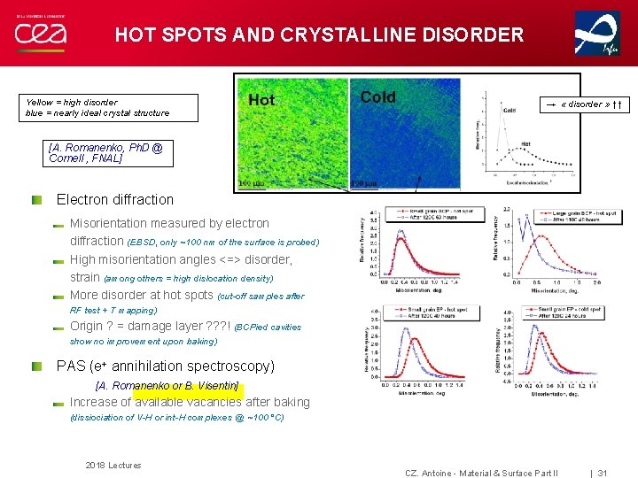
HOT SPOTS AND CRYSTALLINE DISORDER Yellow = high disorder blue = nearly ideal crystal structure → « disorder » ↑↑ [A. Romanenko, Ph. D @ Cornell , FNAL] Electron diffraction Misorientation measured by electron diffraction (EBSD, only ~100 nm of the surface is probed) High misorientation angles <=> disorder, strain (among others = high dislocation density) More disorder at hot spots (cut-off samples after RF test + T mapping) Origin ? = damage layer ? ? ? ! (BCPied cavities show no improvement upon baking) PAS (e+ annihilation spectroscopy) [A. Romanenko or B. Visentin] Increase of available vacancies after baking (dissiociation of V-H or int-H complexes @ ~100 °C) 2018 Lectures CZ. Antoine - Material & Surface Part II | 31
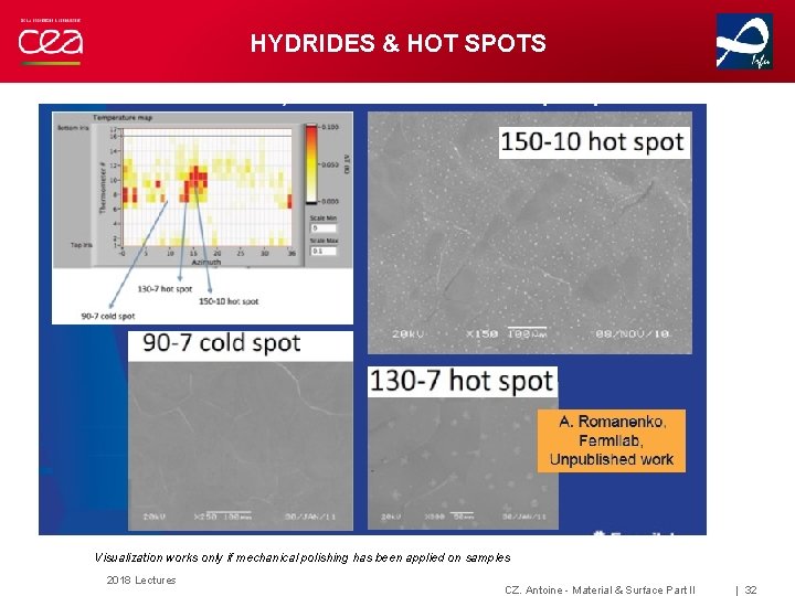
HYDRIDES & HOT SPOTS Visualization works only if mechanical polishing has been applied on samples 2018 Lectures CZ. Antoine - Material & Surface Part II | 32
HYDRIDES 2018 Lectures CZ. Antoine - Material & Surface Part II | PAGE 34
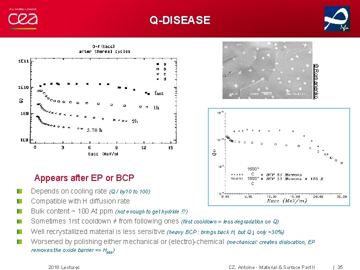
Q-DISEASE © Romanenko ERDA : ~30 nm depth resolution Appears after EP or BCP 1500° C Depends on cooling rate (Q / by 10 to 100) Compatible with H diffusion rate Bulk content ~ 100 At ppm (not enough to get hydride !? ) Sometimes 1 rst cooldown ≠ from following ones (first cooldown = less degradation on Q) Well recrystallized material is less sensitive (heavy BCP : brings back H, but Q ↓ only ~30%) Worsened by polishing either mechanical or (electro)-chemical (mechanical: creates dislocation, EP removes the oxide barrier => Hads) 2018 Lectures CZ. Antoine - Material & Surface Part II | 35
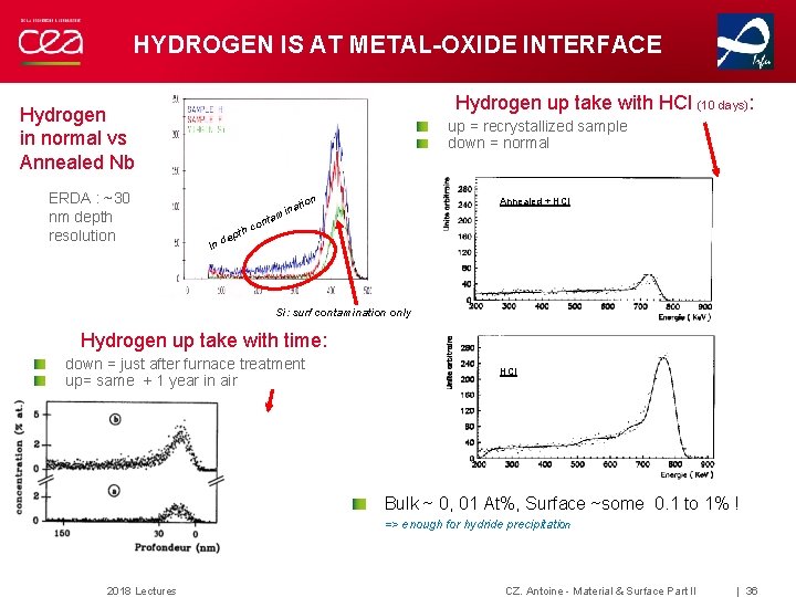
HYDROGEN IS AT METAL-OXIDE INTERFACE Hydrogen up take with HCl (10 days): Hydrogen in normal vs Annealed Nb ERDA : ~30 nm depth resolution up = recrystallized sample down = normal tion Annealed + HCl a min a nt co h t ep In d Si: surf contamination only Hydrogen up take with time: down = just after furnace treatment up= same + 1 year in air HCl Bulk ~ 0, 01 At%, Surface ~some 0. 1 to 1% ! => enough for hydride precipitation 2018 Lectures CZ. Antoine - Material & Surface Part II | 36
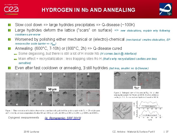
HYDROGEN IN Nb AND ANNEALING Slow cool down => large hydrides precipitates => Q-disease (~100 K) Large hydrides deform the lattice (“scars” on surface) => new dislocations, explain why following cooldowns are worse Worsened by polishing either mechanical or (electro)-chemical (mechanical: creates dislocation, EP removes the oxide barrier => Hads) Annealing (600°C, 7 -10 h) or (800°C, 2 h) => Q-disease cured Some degassing, but there is still a lot of H inside Nb (H comes back @ interface) Main effect = recrystallization : less trapping sites fro H (that’s why recrystallized cavities are less sensitive) Even after fast cooldown or annealing, still hydrides (but less, smaller: no Q-Disease) Cryogenic measurements 2018 Lectures [A. Romanenko, SRF 2013] CZ. Antoine - Material & Surface Part II | 37
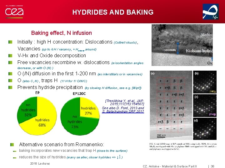
HYDRIDES AND BAKING Baking effect, N infusion Initially : high H concentration: Dislocations (Cottrell clouds), Vacancies (up to 6 H / vacancy, + Hiinterst around) V-Hx and Oxide decomposition Free vacancies recombine w. dislocations (misorientation angles decrease, or with O (N) ) O (/N) diffusion in the first 1 -200 nm (as interstitials or in vacancies) O (also C, N) , traps H (1! H for 1! O/N/C) Prevents hydride precipitation (by slowing H diffusion, see e. g. [Wipf]) [Trenikhina Y, et al, . JAP. 2015; 117(15): 154507] See also D. Ford, 2013 and S. Balachandran SRF 2017 Alternative scenario from Romanenko: baking incorporates new vacancies that trap H (close to the surface) reduces the size of hydrides (many smaller, closer hydrides => ↓ l ) 2018 Lectures CZ. Antoine - Material & Surface Part II | 38
N DOPING/INFUSION • • • 2018 Lectures O = MAIN IMPURITY IN Nb O, N, C = SIMILAR BEHAVIOR IN Nb Influence on hydride precipitates CZ. Antoine - Material & Surface Part II | PAGE 39
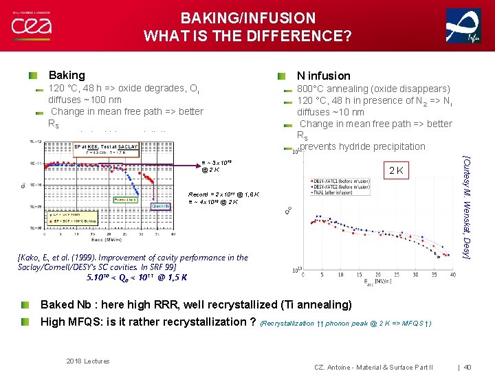
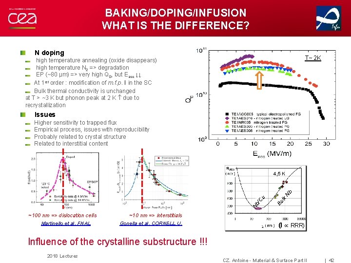
BAKING/INFUSION WHAT IS THE DIFFERENCE? Baking N infusion 120 °C, 48 h => oxide degrades, Oi diffuses ~100 nm Change in mean free path => better RS prevents hydride precipitation 800°C annealing (oxide disappears) 120 °C, 48 h in presence of N 2 => Ni diffuses ~10 nm Change in mean free path => better RS prevents hydride precipitation 2 K Record = 2 x 10¹¹ @ 1, 6 K ≡ ~ 4 x 10¹⁰ @ 2 K [Kako, E. , et al. (1999). Improvement of cavity performance in the Saclay/Cornell/DESY's SC cavities. In SRF 99] 5. 1010 < Q 0 < 1011 @ 1, 5 K [Curtesy M. Wenskat, Desy] ≡ ~ 3 x 10¹⁰ @ 2 K Baked Nb : here high RRR, well recrystallized (Ti annealing) High MFQS: is it rather recrystallization ? (Recrystallization ↑↑ phonon peak @ 2 K => MFQS ↑) 2018 Lectures CZ. Antoine - Material & Surface Part II | 40
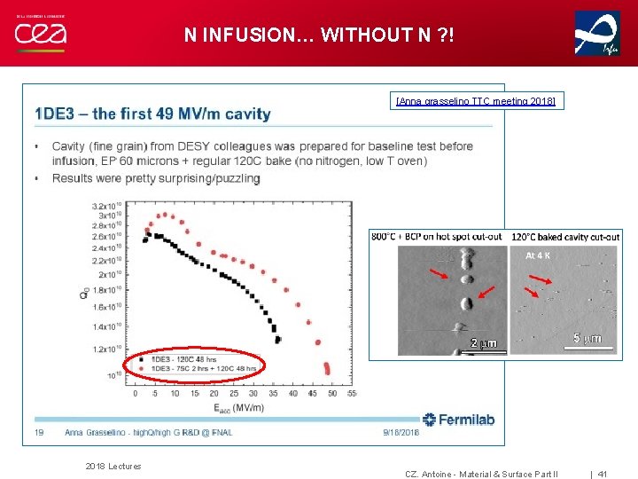
N INFUSION… WITHOUT N ? ! [Anna grasselino TTC meeting 2018] 2018 Lectures CZ. Antoine - Material & Surface Part II | 41
BAKING/DOPING/INFUSION WHAT IS THE DIFFERENCE? N doping T~ 2 K high temperature annealing (oxide disappears) high temperature N 2 => degradation EP (~80 µm) => very high Q 0, but Eacc ↓↓ At 1 rst order : modification of m. f. p. l in the SC Bulk thermal conductivity is unchanged at T > ~3 K but phonon peak at 2 K due to recrystallization Issues Higher sensitivity to trapped flux Empirical process, issues with reproducibility Probably related to crystal structure Related to interstitial content ~100 nm => dislocation cells Martinello et al, FNAL ~10 nm => interstitials Gonella et al, CORNELL U. lk Bu Nb /C u Nb 4, 5 K (l RRR) Influence of the crystalline substructure !!! 2018 Lectures CZ. Antoine - Material & Surface Part II | 42
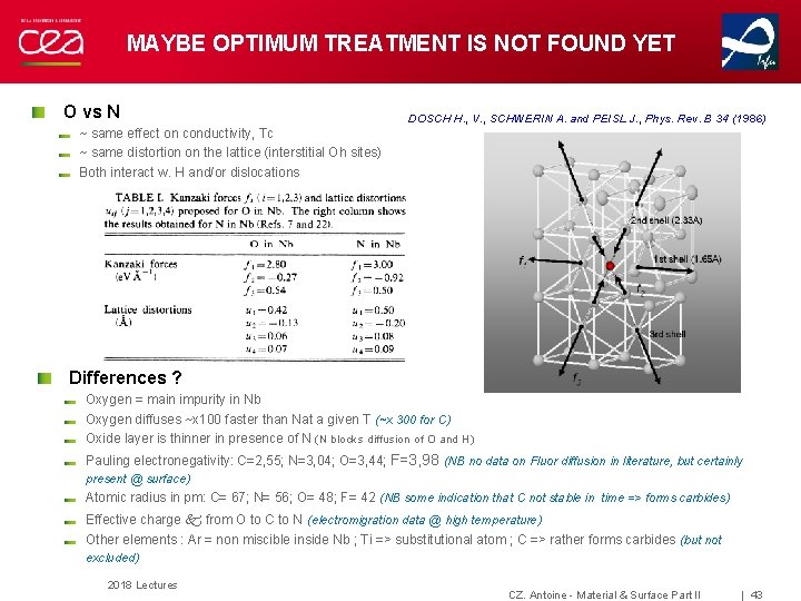
MAYBE OPTIMUM TREATMENT IS NOT FOUND YET O vs N DOSCH H. , V. , SCHWERIN A. and PEISL J. , Phys. Rev. B 34 (1986) ~ same effect on conductivity, Tc ~ same distortion on the lattice (interstitial Oh sites) Both interact w. H and/or dislocations Differences ? Oxygen = main impurity in Nb Oxygen diffuses ~x 100 faster than Nat a given T (~x 300 for C) Oxide layer is thinner in presence of N (N blocks diffusion of O and H) Pauling electronegativity: C=2, 55; N=3, 04; O=3, 44; F=3, 98 (NB no data on Fluor diffusion in literature, but certainly present @ surface) Atomic radius in pm: C= 67; N= 56; O= 48; F= 42 (NB some indication that C not stable in time => forms carbides) Effective charge from O to C to N (electromigration data @ high temperature) Other elements : Ar = non miscible inside Nb ; Ti => substitutional atom ; C => rather forms carbides (but not excluded) 2018 Lectures CZ. Antoine - Material & Surface Part II | 43
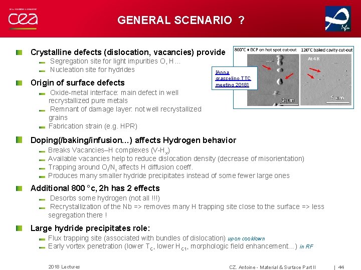
GENERAL SCENARIO ? Crystalline defects (dislocation, vacancies) provide Segregation site for light impurities O, H… Nucleation site for hydrides Origin of surface defects [Anna grasselino TTC meeting 2018] Oxide-metal interface: main defect in well recrystallized pure metals Remnant of damage layer: not well recrystallized grains Fabrication strain (e. g. HPR) Doping(/baking/infusion…) affects Hydrogen behavior Breaks Vacancies–H complexes (V-Hx) Available vacancies help to reduce dislocation density (decrease of misorientation) Trapping around Oi/Ni affects H diffusion coeff. Produces many smaller hydride precipitates instead of some fewer large ones Additional 800 °c, 2 h has 2 effects Desorbs some hydrogen (not all !!!) Recrystallization of the Nb => removes many H trapping site close to the surface => less segregation there ! Large hydride precipitates role: Flux trapping site (associated with bundles of dislocation) upon cooldown Early vortex penetration (lower TC, lower HC 1, morphologic field enhancement…) in RF 2018 Lectures CZ. Antoine - Material & Surface Part II | 44
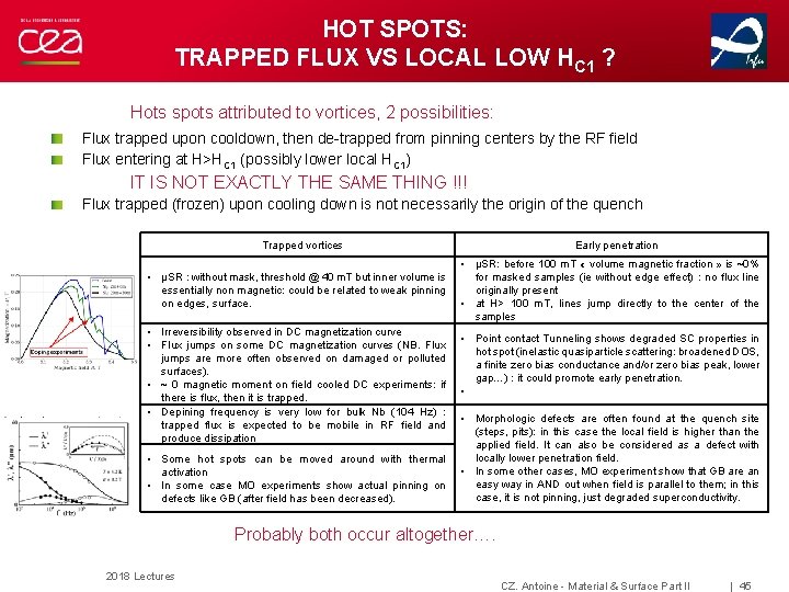
HOT SPOTS: TRAPPED FLUX VS LOCAL LOW HC 1 ? Hots spots attributed to vortices, 2 possibilities: Flux trapped upon cooldown, then de-trapped from pinning centers by the RF field Flux entering at H>HC 1 (possibly lower local HC 1) IT IS NOT EXACTLY THE SAME THING !!! Flux trapped (frozen) upon cooling down is not necessarily the origin of the quench Trapped vortices • µSR : without mask, threshold @ 40 m. T but inner volume is essentially non magnetic: could be related to weak pinning on edges, surface. • Irreversibility observed in DC magnetization curve • Flux jumps on some DC magnetization curves (NB. Flux jumps are more often observed on damaged or polluted surfaces). • ~ 0 magnetic moment on field cooled DC experiments: if there is flux, then it is trapped. • Depining frequency is very low for bulk Nb (104 Hz) : trapped flux is expected to be mobile in RF field and produce dissipation • Some hot spots can be moved around with thermal activation • In some case MO experiments show actual pinning on defects like GB (after field has been decreased). Early penetration • µSR: before 100 m. T « volume magnetic fraction » is ~0% for masked samples (ie without edge effect) : no flux line originally present • at H> 100 m. T, lines jump directly to the center of the samples • Point contact Tunneling shows degraded SC properties in hot spot (inelastic quasiparticle scattering: broadened DOS, a finite zero bias conductance and/or zero bias peak, lower gap…) : it could promote early penetration. • • Morphologic defects are often found at the quench site (steps, pits): in this case the local field is higher than the applied field. It can also be considered as a defect with locally lower penetration field. • In some other cases, MO experiment show that GB are an easy way in AND out when field is parallel to them; in this case, it is not pinning, just degraded superconductivity. Probably both occur altogether…. 2018 Lectures CZ. Antoine - Material & Surface Part II | 45
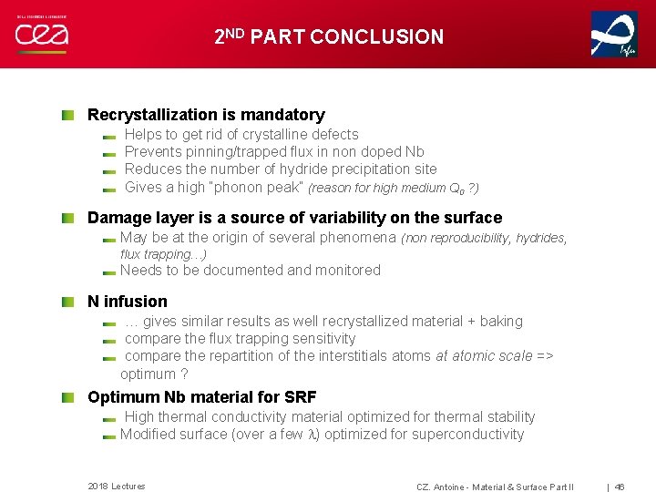
2 ND PART CONCLUSION Recrystallization is mandatory Helps to get rid of crystalline defects Prevents pinning/trapped flux in non doped Nb Reduces the number of hydride precipitation site Gives a high “phonon peak” (reason for high medium Q 0 ? ) Damage layer is a source of variability on the surface May be at the origin of several phenomena (non reproducibility, hydrides, flux trapping…) Needs to be documented and monitored N infusion … gives similar results as well recrystallized material + baking compare the flux trapping sensitivity compare the repartition of the interstitials atoms at atomic scale => optimum ? Optimum Nb material for SRF High thermal conductivity material optimized for thermal stability Modified surface (over a few l) optimized for superconductivity 2018 Lectures CZ. Antoine - Material & Surface Part II | 46
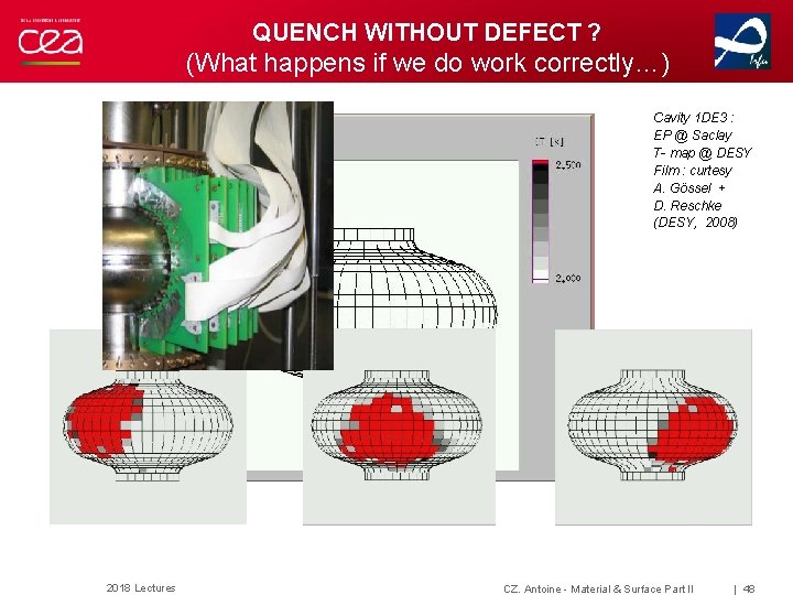
QUENCH WITHOUT DEFECT ? (What happens if we do work correctly…) Cavity 1 DE 3 : EP @ Saclay T- map @ DESY Film : curtesy A. Gössel + D. Reschke (DESY, 2008) 2018 Lectures CZ. Antoine - Material & Surface Part II | 48
T-MAPS & HOT SPOTS Hot spots are observed in cavities at high field Saclay’s ↑, Cornell’s↓ Electropolished cavity 2018 Lectures CZ. Antoine - Material & Surface Part II | 49