Microwave Kinetic Inductance Detectors for Xray Science Antonino





- Slides: 43

Microwave Kinetic Inductance Detectors for X-ray Science Antonino Miceli FNAL Research Techniques Seminar April 24, 2012

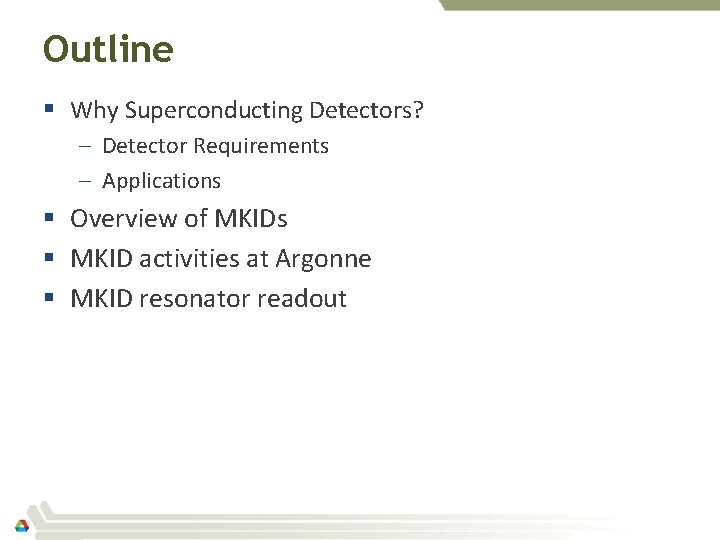
Outline § Why Superconducting Detectors? – Detector Requirements – Applications § Overview of MKIDs § MKID activities at Argonne § MKID resonator readout

Acknowledgements § § Tom Cecil (XSD Staff) Orlando Quaranta (Post-doc) Lisa Gades (XSD Staff) Outside Collaborators: – Professor Ben Mazin (UCSB) – MSD/UChicago TES Team (Novosad et al) – CNM Cleanroom Staff

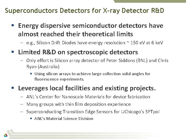
Superconductors Detectors for X-ray Detector R&D § Energy dispersive semiconductor detectors have almost reached their theoretical limits – e. g. , Silicon Drift Diodes have energy resolution ~ 150 e. V at 6 ke. V § Limited R&D on spectroscopic detectors – Only effort is Silicon array detector of Peter Siddons (BNL) and Chris Ryan (Australia) • Using silicon arrays to achieve large collection solid angles for fluorescence experiments. § Leverages local facilities and existing projects. – ANL’s Center for Nanoscale Materials for device fabrication – Many groups with thin film deposition experience – Superconducting Transition Edge Sensors for UChicago’s SPTpol • ANL’s Material Science Division

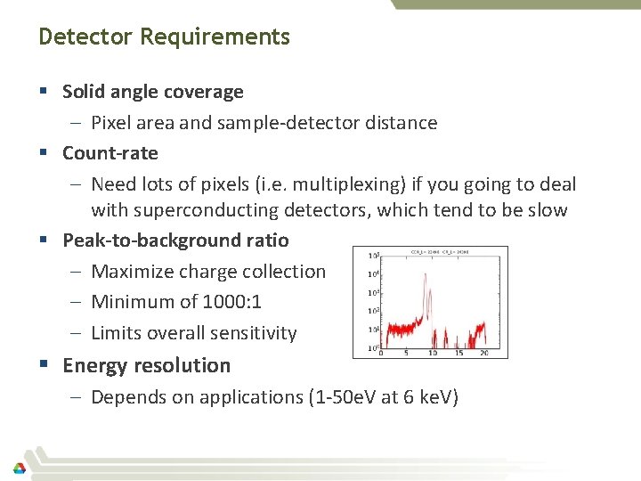
Detector Requirements § Solid angle coverage – Pixel area and sample-detector distance § Count-rate – Need lots of pixels (i. e. multiplexing) if you going to deal with superconducting detectors, which tend to be slow § Peak-to-background ratio – Maximize charge collection – Minimum of 1000: 1 – Limits overall sensitivity § Energy resolution – Depends on applications (1 -50 e. V at 6 ke. V)

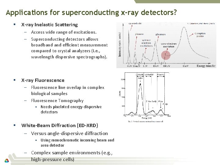
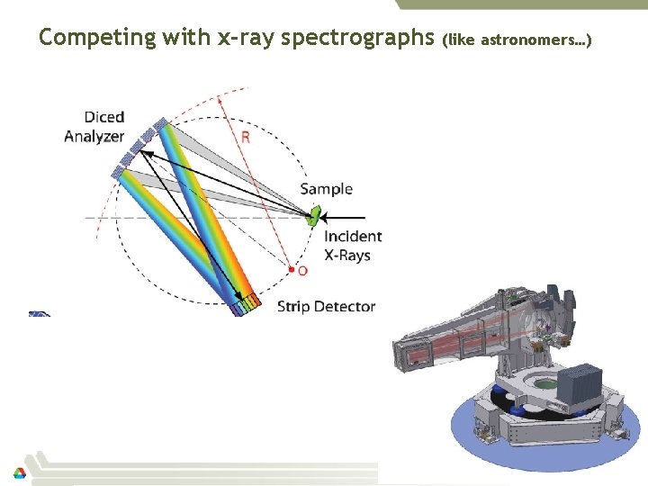
Applications for superconducting x-ray detectors? § X-ray Inelastic Scattering – Access wide range of excitations. – Superconducting detectors allows broadband efficient measurement compared to crystal analyzers (i. e. , wavelength dispersive spectrographs). § X-ray Fluorescence – Fluorescence line overlap in complex biological samples – Fluorescence Tomography • Needs pixelated energy-dispersive detectors § White-Beam Diffraction (ED-XRD) – Versus angle-dispersive diffraction • Using monochromatic incoming beam and area detector – Complex sample environments (e. g. , high-pressure cells)

Competing with x-ray spectrographs (like astronomers…)

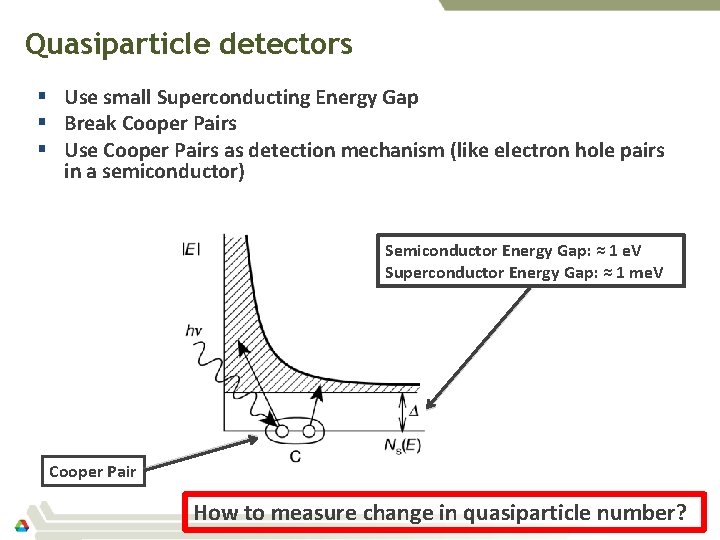
Quasiparticle detectors § Use small Superconducting Energy Gap § Break Cooper Pairs § Use Cooper Pairs as detection mechanism (like electron hole pairs in a semiconductor) Semiconductor Energy Gap: ≈ 1 e. V Superconductor Energy Gap: ≈ 1 me. V Cooper Pair How to measure change in quasiparticle number?

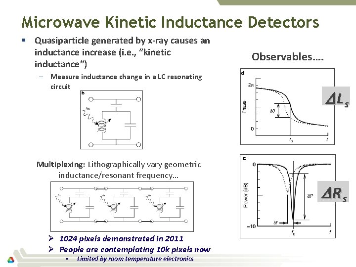
Microwave Kinetic Inductance Detectors § Quasiparticle generated by x-ray causes an inductance increase (i. e. , “kinetic inductance”) – Measure inductance change in a LC resonating circuit Observables…. DLs Multiplexing: Lithographically vary geometric inductance/resonant frequency… DRs Ø 1024 pixels demonstrated in 2011 Ø People are contemplating 10 k pixels now • Limited by room temperature electronics

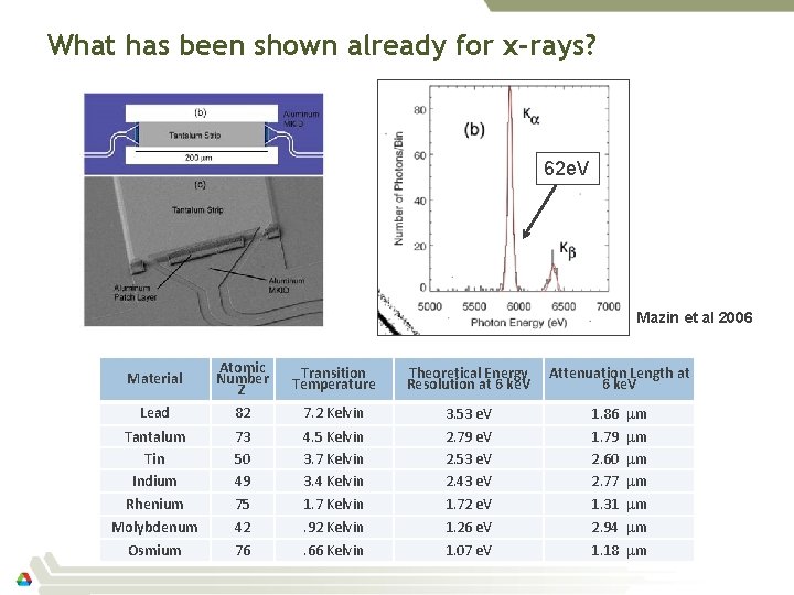
What has been shown already for x-rays? 62 e. V Mazin et al 2006 Material Atomic Number Z Transition Temperature Theoretical Energy Resolution at 6 ke. V Lead 82 7. 2 Kelvin Tantalum Tin Indium Rhenium 73 50 49 75 4. 5 Kelvin 3. 7 Kelvin 3. 4 Kelvin 1. 7 Kelvin 3. 53 e. V 2. 79 e. V 2. 53 e. V 2. 43 e. V 1. 72 e. V 1. 86 1. 79 2. 60 2. 77 1. 31 Molybdenum 42 . 92 Kelvin 1. 26 e. V 2. 94 mm Osmium 76 . 66 Kelvin 1. 07 e. V 1. 18 mm Attenuation Length at 6 ke. V mm mm mm

MKIDs @ Argonne for synchrotrons § The goal is moderate energy resolution (< 20 e. V) with good count rate capabilities (> 200 kcps) (i. e. , ~200 -500 pixels) § Leverages Argonne’s micro/nano-fab facilities (CNM) and superconductivity expertise (MSD); Astronomical TES bolometer program(MSD & UChicago). § Three Main Aspects: 1. Device Fabrication Ø Fabrication is completely in-house Ø Relatively “simple”… patterning of metal (deposition, photolithography, etching) Ø Film quality is very important! Ø Initially aim a simple device, then progress to more complex designs (e. g. , membranesuspended) Ø Dedicated deposition system on order. 2. Cryogenics and Device Characterization Ø We are mostly limited by how fast we can test devices. 3. Readout electronics Ø Initially the analog readout for characterization. Ø Digital FPGA-based array readout in the near future.

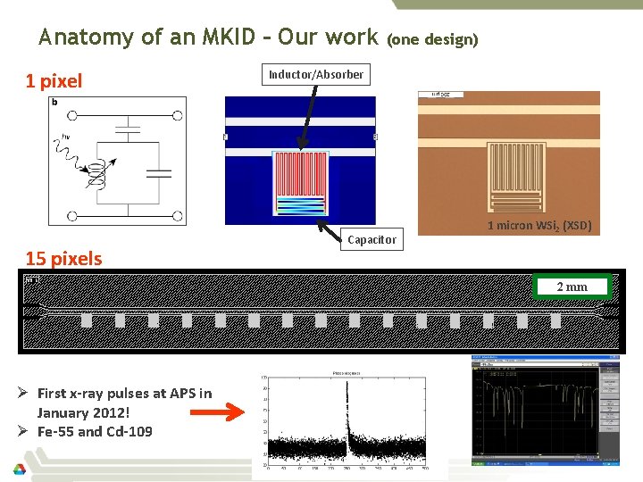
Anatomy of an MKID – Our work 1 pixel 15 pixels (one design) Inductor/Absorber Capacitor 1 micron WSi 2 (XSD) 2 mm Ø First x-ray pulses at APS in January 2012! Ø Fe-55 and Cd-109

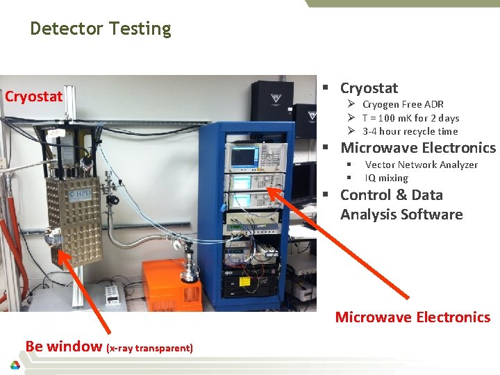
Detector Testing Cryostat § Cryostat Ø Cryogen Free ADR Ø T = 100 m. K for 2 days Ø 3 -4 hour recycle time § Microwave Electronics § § Vector Network Analyzer IQ mixing § Control & Data Analysis Software Microwave Electronics Be window (x-ray transparent)

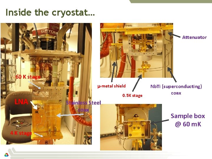
Inside the cryostat… Attenuator 60 K stage m-metal shield LNA 4 K stage 0. 5 K stage Stainless Steel coax Nb. Ti (superconducting) coax Sample box @ 60 m. K

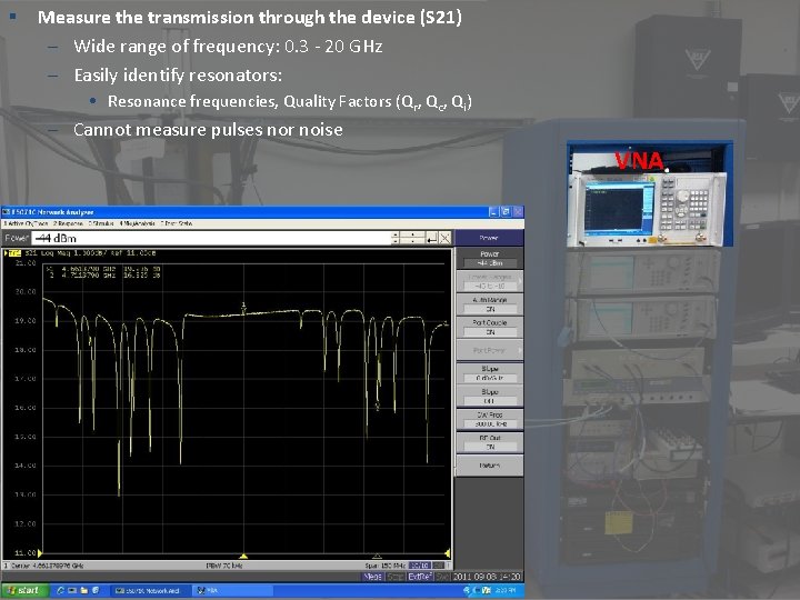
§ Measure the transmission through the device (S 21) – Wide range of frequency: 0. 3 - 20 GHz – Easily identify resonators: • Resonance frequencies, Quality Factors (Qr, Qc, Qi) – Cannot measure pulses nor noise VNA

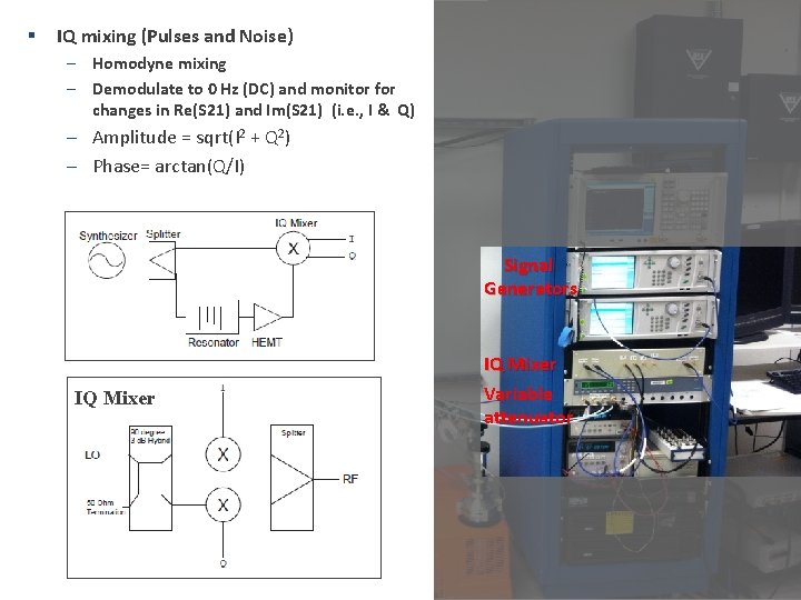
§ IQ mixing (Pulses and Noise) – Homodyne mixing – Demodulate to 0 Hz (DC) and monitor for changes in Re(S 21) and Im(S 21) (i. e. , I & Q) – Amplitude = sqrt(I 2 + Q 2) – Phase= arctan(Q/I) Signal Generators IQ Mixer Variable attenuator

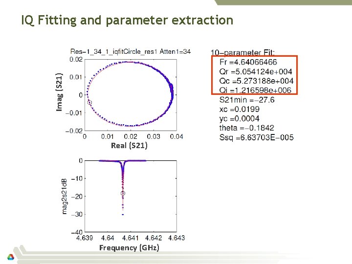
Imag (S 21) IQ Fitting and parameter extraction Real (S 21) Frequency (GHz)

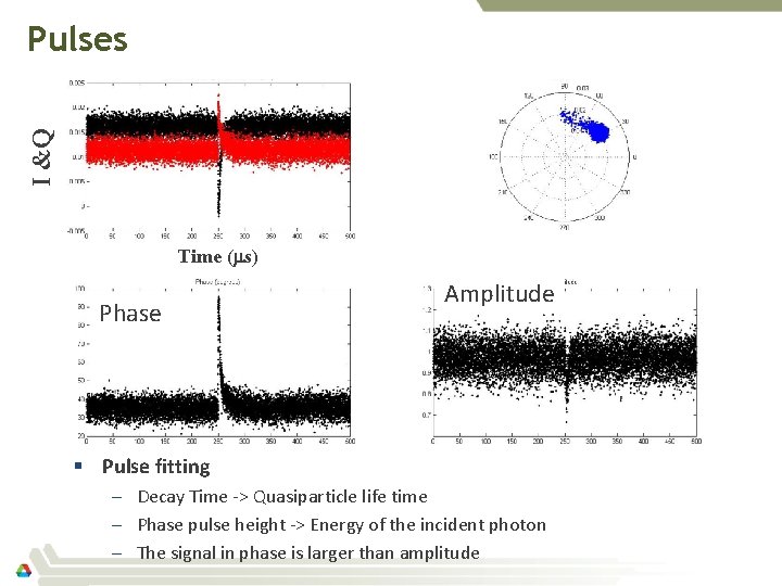
I &Q Pulses Time (ms) Phase Amplitude § Pulse fitting – Decay Time -> Quasiparticle life time – Phase pulse height -> Energy of the incident photon – The signal in phase is larger than amplitude

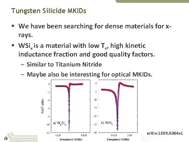
Tungsten Silicide MKIDs § We have been searching for dense materials for xrays. § WSix is a material with low Tc, high kinetic inductance fraction and good quality factors. – Similar to Titanium Nitride – Maybe also be interesting for optical MKIDs. ar. Xiv: 1203. 5064 v 1

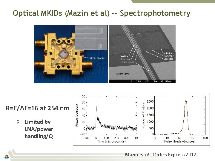
Optical MKIDs (Mazin et al) -- Spectrophotometry R=E/ΔE=16 at 254 nm Ø Limited by LNA/power handling/Q Mazin et al. , Optics Express 2012

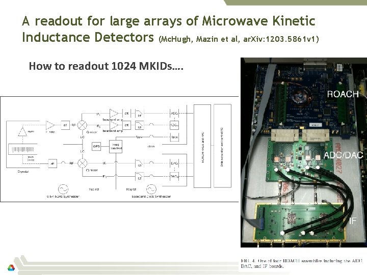
A readout for large arrays of Microwave Kinetic Inductance Detectors (Mc. Hugh, Mazin et al, ar. Xiv: 1203. 5861 v 1) How to readout 1024 MKIDs….

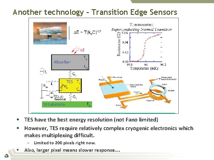
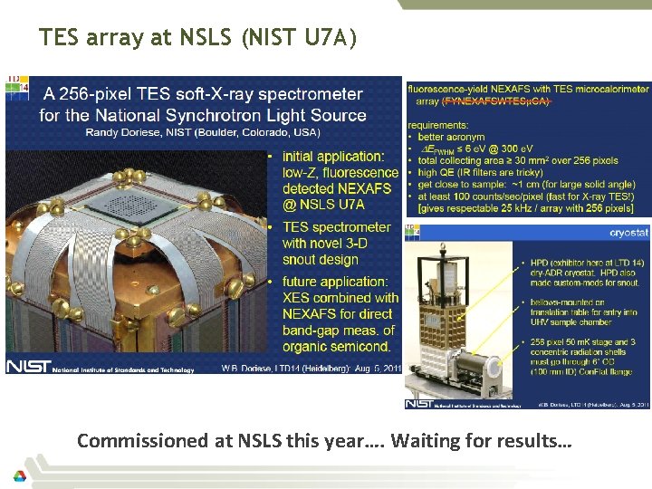
Another technology – Transition Edge Sensors § TES have the best energy resolution (not Fano limited) § However, TES require relatively complex cryogenic electronics which makes multiplexing difficult. – Limited to 200 pixels right now. § Also, larger pixel means slower response….

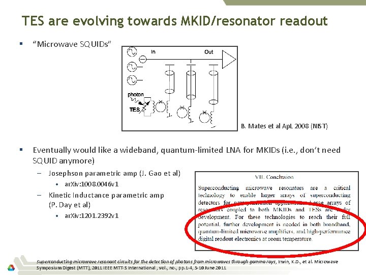
TES are evolving towards MKID/resonator readout § “Microwave SQUIDs” B. Mates et al Ap. L 2008 (NIST) § Eventually would like a wideband, quantum-limited LNA for MKIDs (i. e. , don’t need SQUID anymore) – Josephson parametric amp (J. Gao et al) • ar. Xiv: 1008. 0046 v 1 – Kinetic Inductance parametric amp (P. Day et al) • ar. Xiv: 1201. 2392 v 1 Superconducting microwave resonant circuits for the detection of photons from microwaves through gamma rays, Irwin, K. D. , et al. Microwave Symposium Digest (MTT), 2011 IEEE MTT-S International , vol. , no. , pp. 1 -4, 5 -10 June 2011

Conclusions § Superconducting detector development has started at the APS. – Testing infrastructure (cryo, electronics, analysis software) is complete. – Now focusing on device fabrication and iterating on designs § MKIDs are a path towards high count rates and higher solid angle coverage. – Has the potential to provide a very unique capability (detector/instrument) for the APS. § MKIDs are a relatively young technology and there is room for R&D. § Thank you!

The End

Extra Slides

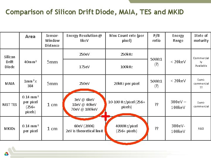
Comparison of Silicon Drift Diode, MAIA, TES and MKID Area Silicon Drift Diode 40 mm 2 MAIA 1 mm 2 x 384 NIST TES 0. 14 mm 2 per pixel (256+ pixels) MKIDs mm 2 0. 14 per pixel Sensor. Window Distance 5 mm Energy Resolution @ 6 ke. V Max Count rate (per pixel) 250 e. V 250 k. Hz 175 e. V 100 k. Hz P/B ratio 5000: 1 (? ) Energy Range State of maturity < 20 ke. V Commercial ly Available < 20 ke. V Semicommercial ? ? 5 mm 250 e. V 20 k. Hz per pixel 5000: 1 (? ) 1 cm 3 e. V @ 6 ke. V 18 e. V @ 40 ke. V 70 e. V @ 100 ke. V 10 -100 Hz/pixel (256+ pixels) ? ? 300 e. V – 100 ke. V Semicommercial 1 cm 60 e. V (2006) 2 e. V is theoretical limit 4000 Hz/pixel (256+ pixels) ? ? 300 e. V 100 ke. V R&D +

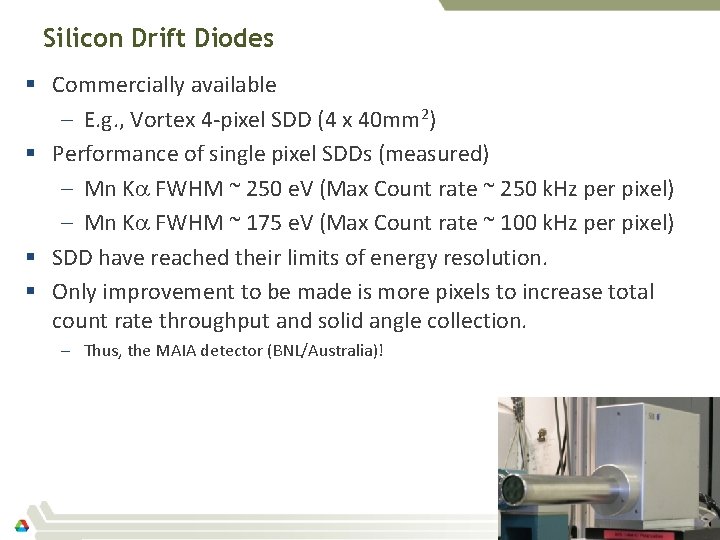
Silicon Drift Diodes § Commercially available – E. g. , Vortex 4 -pixel SDD (4 x 40 mm 2) § Performance of single pixel SDDs (measured) – Mn Ka FWHM ~ 250 e. V (Max Count rate ~ 250 k. Hz per pixel) – Mn Ka FWHM ~ 175 e. V (Max Count rate ~ 100 k. Hz per pixel) § SDD have reached their limits of energy resolution. § Only improvement to be made is more pixels to increase total count rate throughput and solid angle collection. – Thus, the MAIA detector (BNL/Australia)!


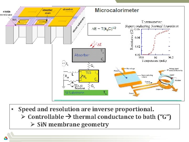
• Speed and resolution are inverse proportional. Ø Controllable thermal conductance to bath (“G”) Ø Si. N membrane geometry

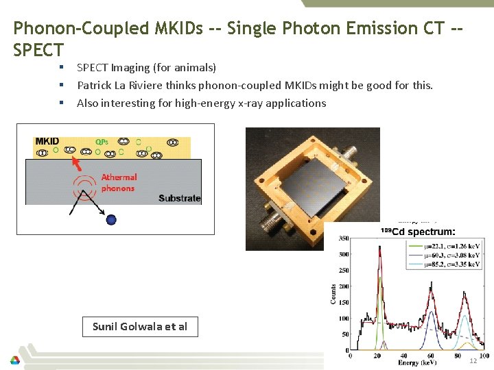
Phonon-Coupled MKIDs -- Single Photon Emission CT -SPECT § § § SPECT Imaging (for animals) Patrick La Riviere thinks phonon-coupled MKIDs might be good for this. Also interesting for high-energy x-ray applications Sunil Golwala et al

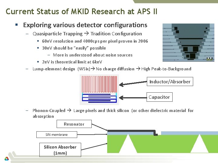
Current Status of MKID Research at APS II § Exploring various detector configurations – Quasiparticle Trapping Tradition Configuration • 60 e. V resolution and 4000 cps per pixel proven in 2006 • 30 e. V should be “easily” possible – More is understood about noise sources • 2 e. V is theoretical limit at 6 ke. V – Lump-element design (WSix) No charge diffusion High Peak-to-Background Inductor/Absorber Capacitor – Phonon-Coupled Large pixels and thick silicon (or other dielectric material for absorption Resonator Si. N membrane Silicon Absorber (1 mm)

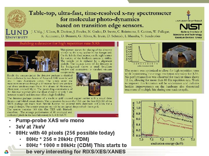
• Pump-probe XAS w/o mono • 3 e. V at 7 ke. V • 80 Hz with 40 pixels (256 possible today) • 80 Hz * 256 = 20 k. Hz (TDM) • 80 Hz * 1000 = 80 k. Hz (CDM) This starts to be very interesting for RIXS/XES/XANES

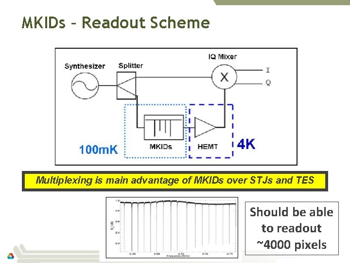
MKIDs – Readout Scheme Multiplexing is main advantage of MKIDs over STJs and TES Should be able to readout ~4000 pixels

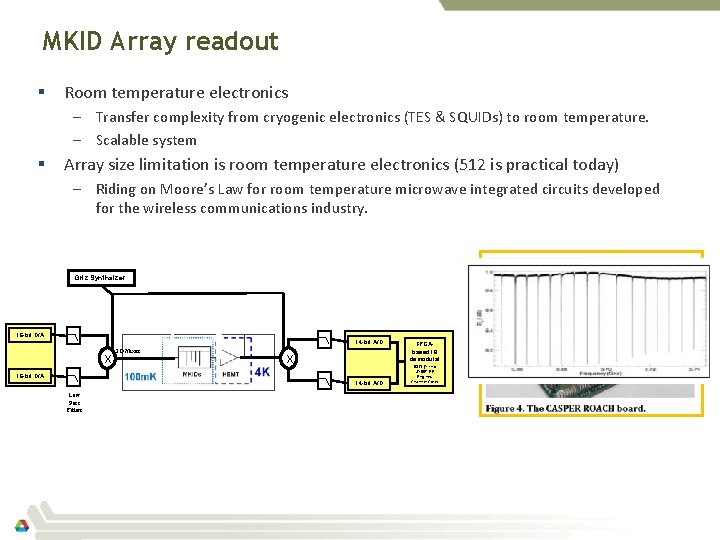
MKID Array readout § Room temperature electronics – Transfer complexity from cryogenic electronics (TES & SQUIDs) to room temperature. – Scalable system § Array size limitation is room temperature electronics (512 is practical today) – Riding on Moore’s Law for room temperature microwave integrated circuits developed for the wireless communications industry. GHz Synthsizer 16 -bit D/A 14 -bit A/D X IQ Mixer X 16 -bit D/A 14 -bit A/D Low Pass Filters FPGAbased IQ demodulat ion (Xilinx SX 95 T RF Engines Channel Core)

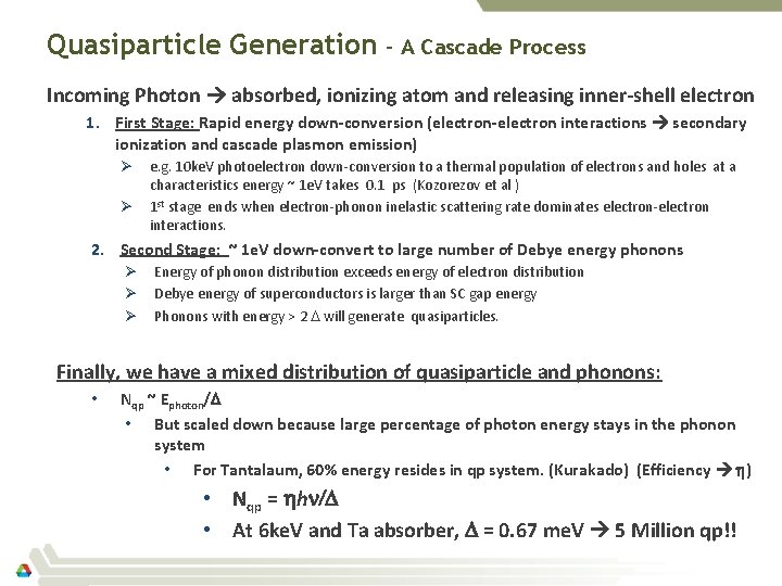
Quasiparticle Generation – A Cascade Process Incoming Photon absorbed, ionizing atom and releasing inner-shell electron 1. First Stage: Rapid energy down-conversion (electron-electron interactions secondary ionization and cascade plasmon emission) Ø Ø e. g. 10 ke. V photoelectron down-conversion to a thermal population of electrons and holes at a characteristics energy ~ 1 e. V takes 0. 1 ps (Kozorezov et al ) 1 st stage ends when electron-phonon inelastic scattering rate dominates electron-electron interactions. 2. Second Stage: ~ 1 e. V down-convert to large number of Debye energy phonons Ø Ø Ø Energy of phonon distribution exceeds energy of electron distribution Debye energy of superconductors is larger than SC gap energy Phonons with energy > 2 D will generate quasiparticles. Finally, we have a mixed distribution of quasiparticle and phonons: • Nqp ~ Ephoton/D • But scaled down because large percentage of photon energy stays in the phonon system • For Tantalaum, 60% energy resides in qp system. (Kurakado) (Efficiency h) • Nqp = hhn/D • At 6 ke. V and Ta absorber, D = 0. 67 me. V 5 Million qp!!

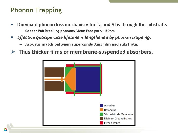
Phonon Trapping § Dominant phonon loss mechanism for Ta and Al is through the substrate. – Copper Pair breaking phonons Mean Free path ~ 50 nm § Effective quasiparticle lifetime is lengthened by phonon trapping. – Acoustic match between superconducting film and substrate. Ø Thus thicker films or membrane-suspended absorbers.

Two major classes of Superconducting Detectors § Thermal Detectors (i. e. , Transition Edge Sensors) § Quasiparticle Detectors

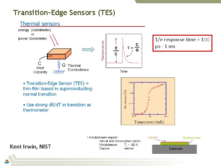
Transition-Edge Sensors (TES) 1/e response time = 100 μs - 1 ms Kent Irwin, NIST

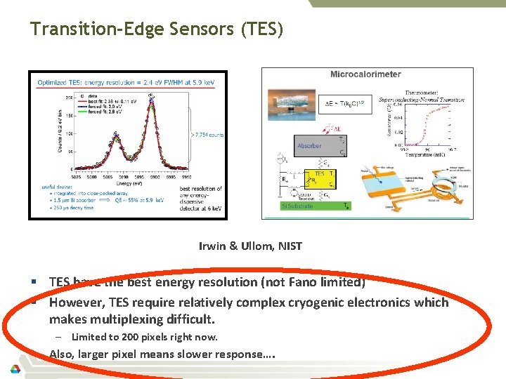
Transition-Edge Sensors (TES) Irwin & Ullom, NIST § TES have the best energy resolution (not Fano limited) § However, TES require relatively complex cryogenic electronics which makes multiplexing difficult. – Limited to 200 pixels right now. § Also, larger pixel means slower response….

TES array at NSLS (NIST U 7 A) Commissioned at NSLS this year…. Waiting for results…

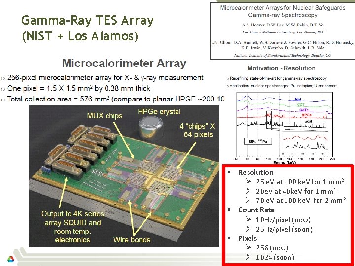
Gamma-Ray TES Array (NIST + Los Alamos) § Resolution Ø 25 e. V at 100 ke. V for 1 mm 2 Ø 20 e. V at 40 ke. V for 1 mm 2 Ø 70 e. V at 100 ke. V for 2 mm 2 § Count Rate Ø 10 Hz/pixel (now) Ø 25 Hz/pixel (soon) § Pixels Ø 256 (now) Ø 1024 (soon)