Landscape for SRF Thin Films Larry Phillips July
- Slides: 16

Landscape for SRF Thin Films Larry Phillips July 18, 2012

WHY THIN FILMS • • • Cost is the only driver Lower cost enables many new applications Future applications of SRF linacs for which cost is a driver: ILC, or LEP 3, ADS, medical, light sources, …. Of these, an ADS proton linac is most fascinating; it will be the first major industrial accelerator market in the world, giving potential companies two valuable opportunities: 1. They will see a large ongoing market 2. They can not only own the technology, but own as well their own internal resources for innovation to compete in that market.

WHY DO THIN FILMS LOWER COST? - Thin film niobium cavity substrates are of highly formable metals, such as copper or aluminum. - Enables integration of many system functions in a single low-cost structure, i. e. an aluminum casting. - Integrated functions: • Cavity RF surface definition • High thermal conductivity substrate • Helium vessel • Cryogenic manifold with heat exchanger • Cavity stiffening, and many more……….

CAST CAVITY IMPLICATIONS - High precision and stability compared to sheet metal - Field flatness and cell alignment built in. - No variation in cavity length from field flatness tuning - Very small tuning range required (small local perturbation or reactive tuner) - Not sensitive to helium pressure variations - Insensitive to Lorentz force detuning

CAST CAVITY IMPLICATIONS cont. - No microphonics - No financial and environmental cost burden from acids - Lower RF power consumption–no need for microphonic head room.

II. Where are we on the road to high quality thin film cavities? - What went wrong in the past? Why Q-drop? - What were the visible differences between bulk niobium and niobium made with conventional magnetron sputtering? - The only visible differences were loose, voided surface structure and low RRR, which were well known features of magnetron sputtering of high melting point metals. But this was all that was available at the time.

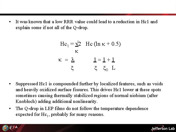
• It was known that a low RRR value could lead to a reduction in Hc 1 and explain some if not all of the Q-drop. Hc 1 = 2 Hc (ln + 0. 5) = 1=1+1 0 L • Suppressed Hc 1 is compounded further by localized features, such as voids and heavily oxidized surface fissures. This drives Hc 1 lower at these spots sometimes causing thermally stabilized regions of normal niobium (after Knobloch) adding additional nonlinearity. • The Q-drop in LEP films do not follow the temperature dependence expected for Hc 1, probably for many reasons.

At JLab a new effort was launched with two main features: 1. A new niobium deposition process was developed using “energetic condensation” with a niobium ECR plasma in vacuum. (Thesis of Genfa Wu) 2. The process would be developed using small samples by correlating: a) Deposition parameters b) Film microstructure c) SRF performance A great value was placed on the development of an understanding before trying to make cavities.

III. Where things are today. After much work, how do films made by “energetic condensation” and magnetron sputtering compare today? A. Conventional Magnetron Sputtering - 10 <RRR<25 - Surface voids are sources of B field enhancement.

B. Energetic Condensation • An extensive map of deposition parameters, film structure, substrate temperature, and RRR has been developed • Films made today having 200 <RRR <400 can be made repetitively on many substrate materials, including copper • Smooth, dense films are obtained • This effort has been highly successful!!!!!! • If the depression of Hc 1 and field enhancement by surface features were dominating Q drop, these problems are solved. • But what else might be there?

IV. Unknown Problems In addition to the known problems with conventional magnetron sputtering, are there any hidden causes of Q-drop waiting to be discovered? and what might they be? 1. RF residual resistance- not understood - Few measurements exist on energetically condensed films—not yet conclusive— more to come. 2. SRF surface and copper substrate are only ~1 micron apart separated by straight grain boundaries along columnar films.

IV. Unknown Problems – cont. Diffusion within grain boundaries can be 104 – 105 higher than surface diffusion. Typical substrate temperatures for copper are Ts/Tm~0. 5 3. Surface oxidation—unknown effect on niobium films. Easy solutions to known “Unknown Problems” - Diffusion barrier between substrate and film - Dielectric diffusion barrier on RF surface, or plasma oxidized Nb 2 05 –no sub oxides.

V. Three Future Tasks 1. Understand the physics of residual RF surface impedance and its dependence on deposition parameters for thin Nb films 2. Refine small sample Rs measuring process. The development of both niobium films and ML films will depend on this. A higher rate of sample testing is needed. The calorimetric cavity process with high resolution are especially valuable for RF residual resistivity studies.

3. Fiber growth films - In recent years much attention has been given to hetero epitaxial growth modes. This makes sense since there is much to learn quickly about the effect of deposition parameters on crystal quality, for instance, by growing large crystals on wellcharacterized substrates. Fiber growth is the default mode when depositing on an amorphous surface. Grains having crystal planes with the lowest surface energy exposed to the incident flux will grow faster and “pinch out” competing grains, resulting in grain diameters of fixed column size after the competition is complete.

To use this growth mode, the average grain diameter at the RF surface much be large enough that Hc 1 is not affected by grain boundary scattering. - Why bother? - From a manufacturing point of view this, would be the simplest and least critical process, given the caveat of grain size. - the only starting surface requirement is that it be clean and smooth. - initial “ion stitching” increases shear strength at the substrate interface and allows a greater film thickness. - An extra thick amorphous layer at substrate provides a diffusion barrier for free and more.

CONCLUSIONS • High quality niobium films can be produced using energetic condensation techniques • Thin film cavity/linac structures have very large cost reduction potential over conventional bulk niobium structures • Such low structure costs will drive the economic optimum to lower real estate gradients and lower volt per dollar values • Thank you on behalf of the JLAB thin film group.