SRF ACCELERATING CAVITIES RD SRF MULTILAYERS INVESTIGATIONS G
- Slides: 12

SRF ACCELERATING CAVITIES R&D: SRF MULTILAYERS INVESTIGATIONS G. Martinet, C. Baumier (IPN), F. Fortuna (CSNSM) C. Antoine (Irfu) 12 September 2013 1

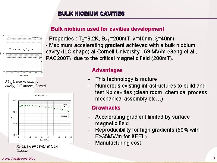
BULK NIOBIUM CAVITIES Bulk niobium used for cavities development - Properties : TC=9. 2 K, BC 1=200 m. T, λ=40 nm, ξ=40 nm - Maximum accelerating gradient achieved with a bulk niobium cavity (ILC shape) at Cornell University : 59 MV/m (Geng et al. , PAC 2007) due to the critical magnetic field (200 m. T). Advantages Single cell re-entrant cavity, ILC shape, Cornell - This technology is mature - Numerous existing infrastructures to build and test Nb cavities (clean room, chemical process, mechanical assembly etc…) Drawbacks XFEL 9 -cell cavity at CEA Saclay mardi 7 septembre 2021 - Accelerating gradient limited by surface magnetic field - Reproducibility for high gradients (60% with E>35 MV/m for XFEL) - Manufacturing cost 3

SUPERCONDUCTING LAYERS ON COPPER Superconducting layer on copper as first alternative Layer of thickness 3 -5µm is sputtered on copper substrate already use for several facilities (Soleil, LEP 200, ALPI) Advantages: - manufacturing cost reduction - Better RF performances at low field - Better stability (thermal, mechanic, magnetic. . ) Issues - Anomalous losses increase roughly at medium field (15 MV/m) - Limited to coat simple shape Other solutions must be investigated 13 September 2013 4

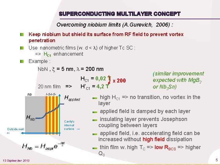
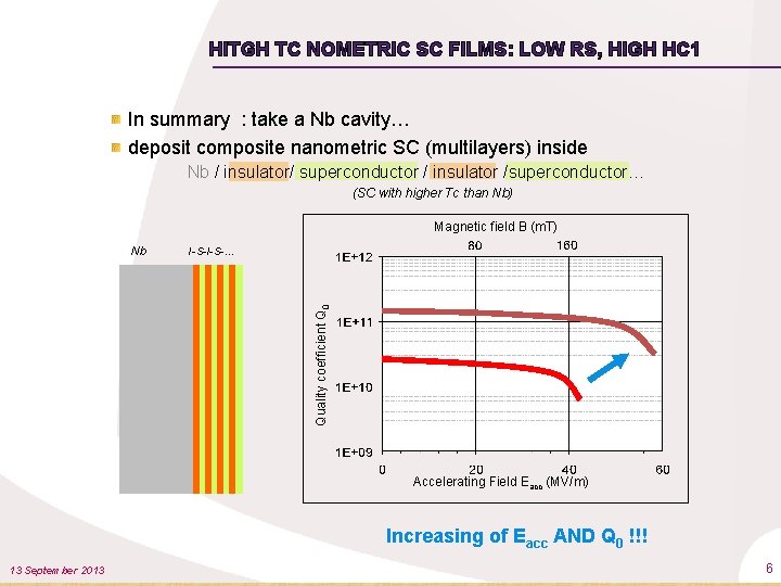
SUPERCONDUCTING MULTILAYER CONCEPT Overcoming niobium limits (A. Gurevich, 2006) : Keep niobium but shield its surface from RF field to prevent vortex penetration Use nanometric films (w. d < l) of higher Tc SC : => HC 1 enhancement Example : Nb. N , x = 5 nm, l = 200 nm 20 nm film => Nb HNb Outside wall 13 September 2013 I-S- Happlied Cavity's internal surface → HC 1 = 0, 02 T x 200 H’C 1 = 4, 2 T (similar improvement expected with Mg. B 2 or Nb 3 Sn) high HC 1 => no transition, no vortex in the layer applied field is damped by each layer insulating layer prevents Josephson coupling between layers applied field, i. e. accelerating field can be increased without high field dissipation thin film w. high TC => low RBCS => higher Q 0 5

HITGH TC NOMETRIC SC FILMS: LOW RS, HIGH HC 1 In summary : take a Nb cavity… deposit composite nanometric SC (multilayers) inside Nb / insulator/ superconductor / insulator /superconductor… (SC with higher Tc than Nb) Magnetic field B (m. T) I-S-… Quality coefficient Q 0 Nb Accelerating Field Eacc (MV/m) Increasing of Eacc AND Q 0 !!! 13 September 2013 6

P 2 IO SUPPORT: EXPERIMENTAL INVESTIGATION Produce reference multilayer samples CSNSM upgrades epitaxial set up with ECR source to produce (Nb. N/Al. N) on niobium substrate Characterize multilayer sample - Chemical and structure analysis at CSNSM - Magnetometric measurements at Irfu - RF Rs measurement at IPN 13 September 2013 7

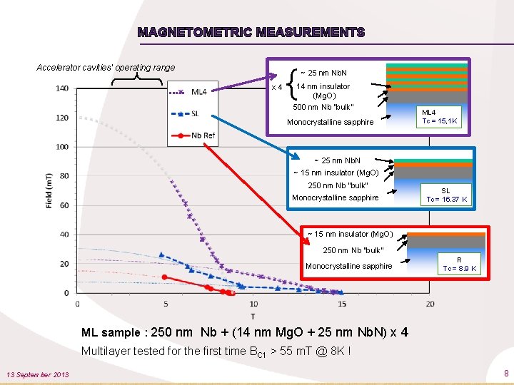
MAGNETOMETRIC MEASUREMENTS Accelerator cavities' operating range ~ 25 nm Nb. N x 4 14 nm insulator (Mg. O) 500 nm Nb “bulk” Monocrystalline sapphire ML 4 Tc = 15, 1 K ~ 25 nm Nb. N ~ 15 nm insulator (Mg. O) 250 nm Nb “bulk” Monocrystalline sapphire SL Tc = 16. 37 K ~ 15 nm insulator (Mg. O) 250 nm Nb “bulk” Monocrystalline sapphire R Tc = 8. 9 K ML sample : 250 nm Nb + (14 nm Mg. O + 25 nm Nb. N) x 4 Multilayer tested for the first time BC 1 > 55 m. T @ 8 K ! 13 September 2013 8

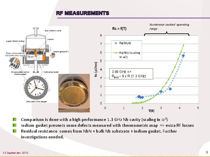
RF MEASUREMENTS Accelerator cavities' operating range 3. 88 GHz => RBCS~ 9 x R (1. 3 GHz) Comparison is done with a high performance 1. 3 GHz Nb cavity (scaling in w 2) Indium gasket presents some defects measured with thermometric map => extra RF losses Residual resistance comes from Nb. N + bulk Nb substrate + indium gasket. Further investigations needed. 13 September 2013 9

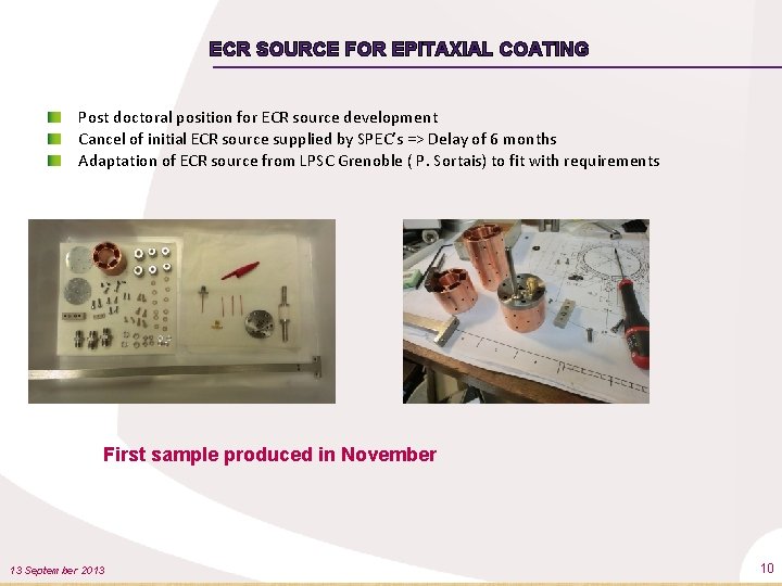
ECR SOURCE FOR EPITAXIAL COATING Post doctoral position for ECR source development Cancel of initial ECR source supplied by SPEC’s => Delay of 6 months Adaptation of ECR source from LPSC Grenoble ( P. Sortais) to fit with requirements First sample produced in November 13 September 2013 10

CONCLUSIONS AND PERSPECTIVES 13 September 2013 • ML structures seem to be a promising way to go beyond Nb for accelerator cavities • Renewed activity on bulk-like Nb films (cost issues) and high HSH SC e. g. Nb 3 Sn or Nb. N (higher performances) • Look for higher Q 0, not only Eacc ! • P 2 IO allowed enforcing experimental investigation on SC multilyayers for SRF applications 11

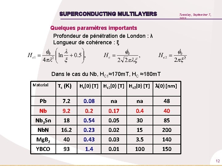
SUPERCONDUCTING MULTILAYERS Tuesday, September 7, 2021 Quelques paramètres importants Profondeur de pénétration de London : λ Longueur de cohérence : ξ Dans le cas du Nb, HC 1≈170 m. T, HC ≈180 m. T Material Tc (K) Hc(0) [T] Hc 1(0) [T] Hc 2(0) [T] (0) [nm] Pb 7. 2 0. 08 na na 48 Nb 9. 2 0. 17 0. 4 40 Nb 3 Sn 18 0. 54 0. 05 30 85 Nb. N 16. 2 0. 23 0. 02 15 200 Mg. B 2 40 0. 43 0. 03 3. 5 140 YBCO 93 1. 4 0. 01 100 150 12

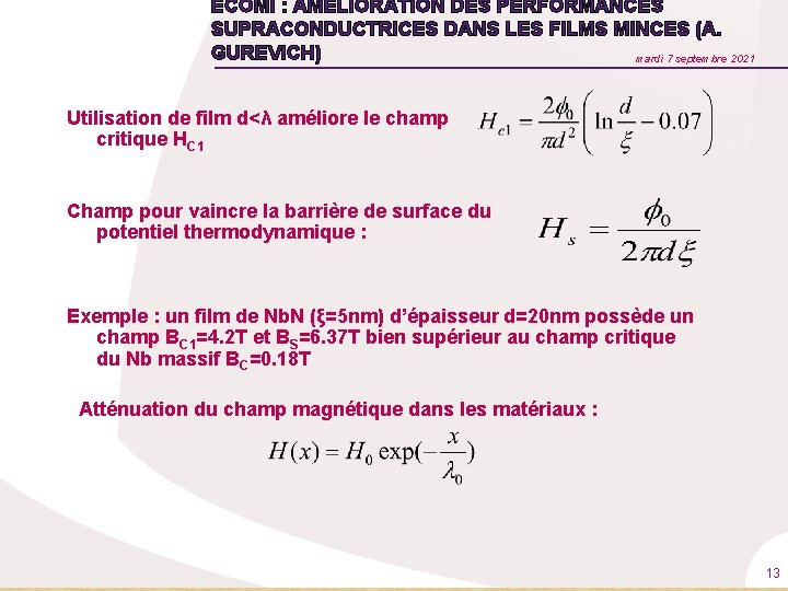
ECOMI : AMÉLIORATION DES PERFORMANCES SUPRACONDUCTRICES DANS LES FILMS MINCES (A. GUREVICH) mardi 7 septembre 2021 Utilisation de film d<λ améliore le champ critique HC 1 Champ pour vaincre la barrière de surface du potentiel thermodynamique : Exemple : un film de Nb. N (ξ=5 nm) d’épaisseur d=20 nm possède un champ BC 1=4. 2 T et BS=6. 37 T bien supérieur au champ critique du Nb massif BC=0. 18 T Atténuation du champ magnétique dans les matériaux : 13