Status of the ASD preamp for MDT RO
![ADC vs. run-down current code: improved Max. width: 170+-50 ns ADC pulse width[ns] ch ADC vs. run-down current code: improved Max. width: 170+-50 ns ADC pulse width[ns] ch](https://slidetodoc.com/presentation_image/164aeec54d94cc37e4dca8c3a204d631/image-20.jpg)
![Power consumption vs. Vcc Power [m. W] • 600 • 550 • 500 • Power consumption vs. Vcc Power [m. W] • 600 • 550 • 500 •](https://slidetodoc.com/presentation_image/164aeec54d94cc37e4dca8c3a204d631/image-22.jpg)
![Peak at Monitor output [m. V] Gain matching between different ASDv 5 chips Input Peak at Monitor output [m. V] Gain matching between different ASDv 5 chips Input](https://slidetodoc.com/presentation_image/164aeec54d94cc37e4dca8c3a204d631/image-23.jpg)
- Slides: 29

Status of the ASD preamp for MDT R/O in Phase-II Preliminary Design Review, sept. , 05, 2017 Robert Richter, MPI Munich

People involved S. Abovyan, V. Danielyan, M. Fras, O. Kortner, H. Kroha, B. Weber*, Y. Zhao, RR Max-Planck-Institute for Physics, Munich A. Baschirotto, M. de Matteis, F. Resta University of Milano-Bicocca C. Valderanis LMU Munich * 05 -sept-2017 now at the INTEL corporation, Germany PDR of the ASDv 6 chip for MDT Readout R. Richter 2

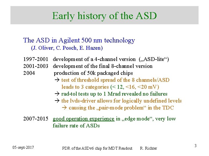
Early history of the ASD The ASD in Agilent 500 nm technology (J. Oliver, C. Posch, E. Hazen) 1997 -2001 development of a 4 -channel version („ASD-lite“) 2001 -2003 development of the final 8 -channel version 2004 production of 50 k packaged chips test of threshold spread of the 8 channels/ASD leads to 3 categories (< 12, <16, <20 m. V) rad-tol tests up to 1 Mrad revealed no failures the lvds-driver allows for logically undefined levels causing the „pair-mode problem“ in the TDC 2007 -2015 good operation experience in „edge mode“, very low failure rate of ASDs 05 -sept-2017 PDR of the ASDv 6 chip for MDT Readout R. Richter 3

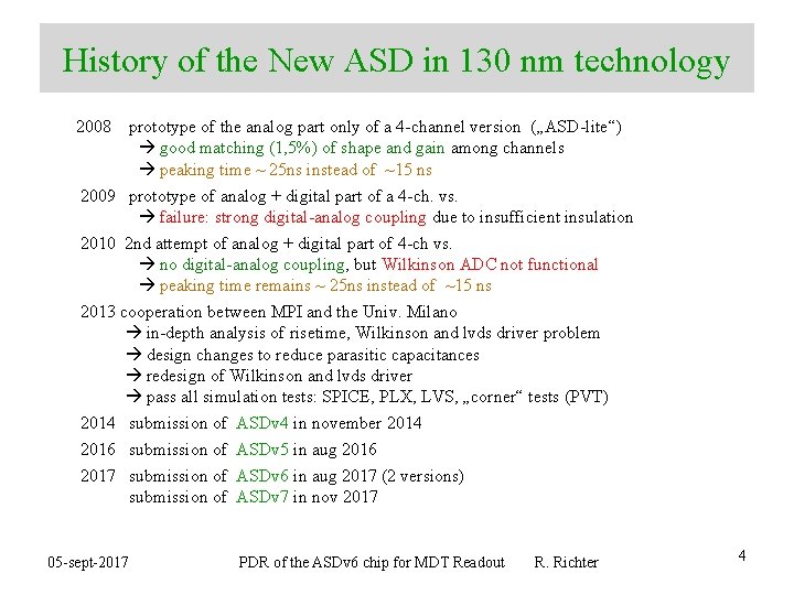
History of the New ASD in 130 nm technology 2008 prototype of the analog part only of a 4 -channel version („ASD-lite“) good matching (1, 5%) of shape and gain among channels peaking time ~ 25 ns instead of ~15 ns 2009 prototype of analog + digital part of a 4 -ch. vs. failure: strong digital-analog coupling due to insufficient insulation 2010 2 nd attempt of analog + digital part of 4 -ch vs. no digital-analog coupling, but Wilkinson ADC not functional peaking time remains ~ 25 ns instead of ~15 ns 2013 cooperation between MPI and the Univ. Milano in-depth analysis of risetime, Wilkinson and lvds driver problem design changes to reduce parasitic capacitances redesign of Wilkinson and lvds driver pass all simulation tests: SPICE, PLX, LVS, „corner“ tests (PVT) 2014 submission of ASDv 4 in november 2014 2016 submission of ASDv 5 in aug 2016 2017 submission of ASDv 6 in aug 2017 (2 versions) submission of ASDv 7 in nov 2017 05 -sept-2017 PDR of the ASDv 6 chip for MDT Readout R. Richter 4

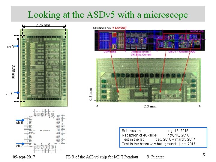
Looking at the ASDv 5 with a microscope 2. 26 mm ch 0 3. 38 mm ch 7 ch 0 ch 7 05 -sept-2017 Submission: aug, 15, 2016 Reception of 40 chips: nov, 10, 2016 Test in the lab: dec, 2016 – march, 2017 Test in the beam w. g-background: june, 2017 PDR of the ASDv 6 chip for MDT Readout R. Richter 5

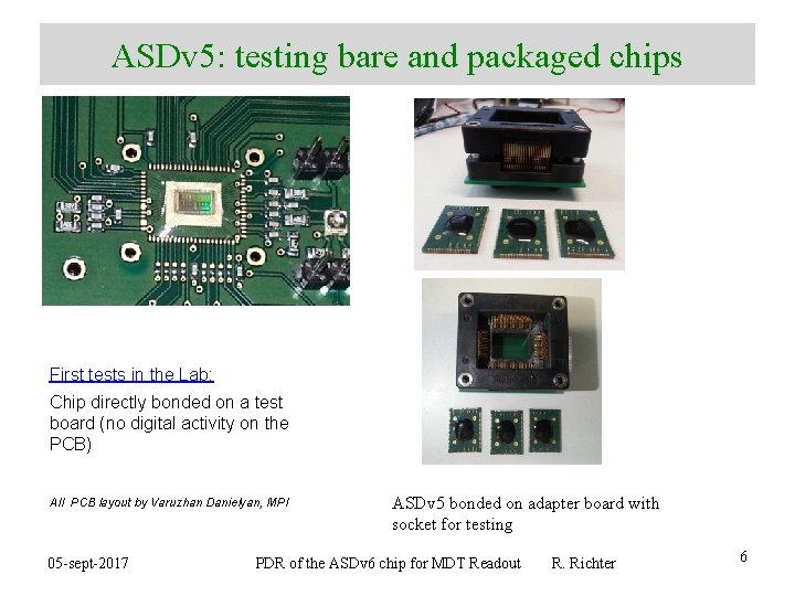
ASDv 5: testing bare and packaged chips First tests in the Lab: Chip directly bonded on a test board (no digital activity on the PCB) All PCB layout by Varuzhan Danielyan, MPI 05 -sept-2017 ASDv 5 bonded on adapter board with socket for testing PDR of the ASDv 6 chip for MDT Readout R. Richter 6

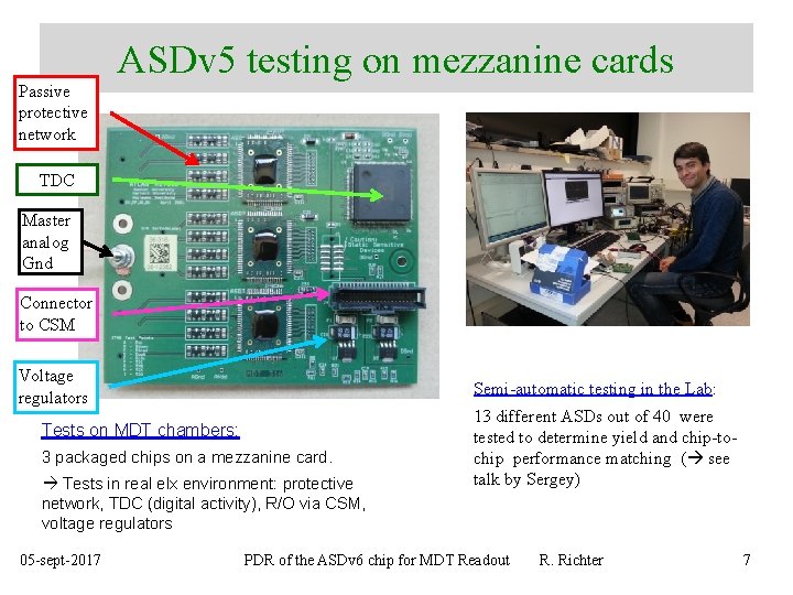
ASDv 5 testing on mezzanine cards Passive protective network TDC Master analog Gnd Connector to CSM Voltage regulators Semi-automatic testing in the Lab: Tests on MDT chambers: 3 packaged chips on a mezzanine card. Tests in real elx environment: protective network, TDC (digital activity), R/O via CSM, voltage regulators 05 -sept-2017 13 different ASDs out of 40 were tested to determine yield and chip-tochip performance matching ( see talk by Sergey) PDR of the ASDv 6 chip for MDT Readout R. Richter 7

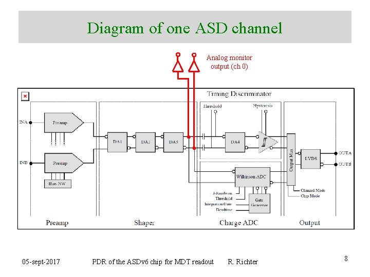
Diagram of one ASD channel Analog monitor output (ch 0) 05 -sept-2017 PDR of the ASDv 6 chip for MDT readout R. Richter 8

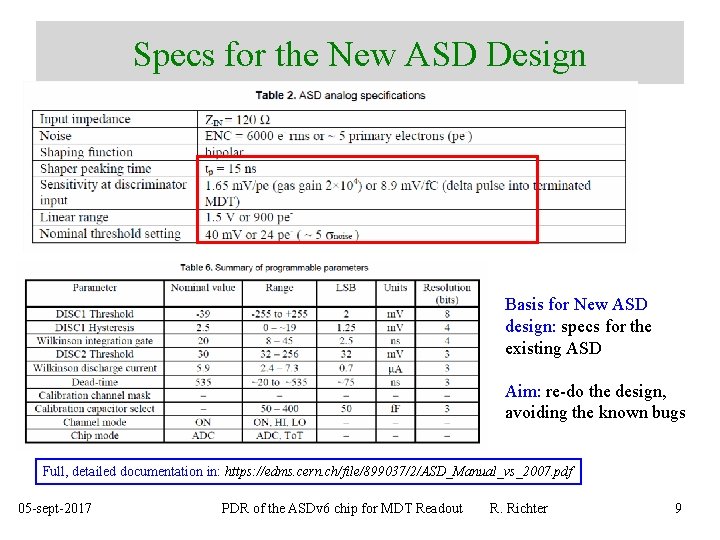
Specs for the New ASD Design Basis for New ASD design: specs for the existing ASD Aim: re-do the design, avoiding the known bugs Full, detailed documentation in: https: //edms. cern. ch/file/899037/2/ASD_Manual_vs_2007. pdf 05 -sept-2017 PDR of the ASDv 6 chip for MDT Readout R. Richter 9

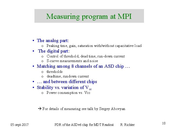
Measuring program at MPI • The analog part: o Peaking time, gain, saturation with/without capacitative load • The digital part: o Control of threshold, dead time, run-down current o S-curve measurements and noise • Matching among 8 channels of an ASD chip … o thresholds o deadtime, rundown current • … and between different chips • Stability vs. variation of Vcc o Power consumption vs. Vcc For details of measuring see talk by Sergey Abovyan 05 -sept-2017 PDR of the ASDv 6 chip for MDT Readout R. Richter 10

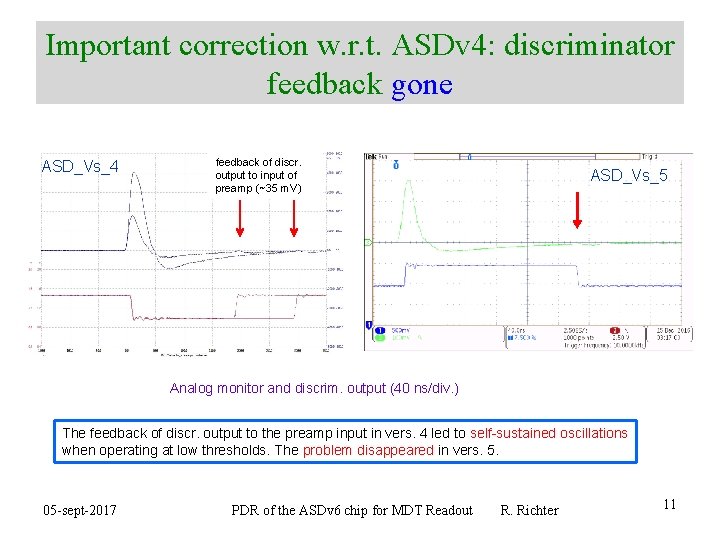
Important correction w. r. t. ASDv 4: discriminator feedback gone ASD_Vs_4 feedback of discr. output to input of preamp (~35 m. V) ASD_Vs_5 Analog monitor and discrim. output (40 ns/div. ) The feedback of discr. output to the preamp input in vers. 4 led to self-sustained oscillations when operating at low thresholds. The problem disappeared in vers. 5. 05 -sept-2017 PDR of the ASDv 6 chip for MDT Readout R. Richter 11

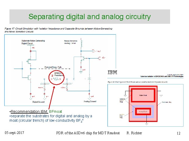
Separating digital and analog circuitry • Recommendation IBM: BFmoat • separate the substrates for digital and analog by a moat (circular trench) of low-conductivity BF 2+ 05 -sept-2017 PDR of the ASDv 6 chip for MDT Readout R. Richter 12

Peaking time, gain, linearity and saturation behaviour 05 -sept-2017 PDR of the ASDv 6 chip for MDT Readout R. Richter 13

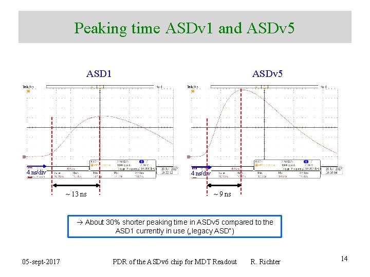
Peaking time ASDv 1 and ASDv 5 ASD 1 4 ns/div ASDv 5 Peaking time ASD 1 at 50 f. C 4 ns/div ~ 13 ns ~ 9 ns About 30% shorter peaking time in ASDv 5 compared to the ASD 1 currently in use („legacy ASD“) 05 -sept-2017 PDR of the ASDv 6 chip for MDT Readout R. Richter 14

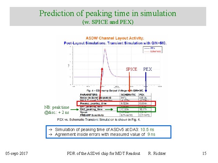
Prediction of peaking time in simulation (w. SPICE and PEX) SPICE PEX NB: peak time @disc. : + 2 ns Simulation of peaking time of ASDv 5 at DA 3: 10. 5 ns Agreement inside errors with measured value of 9 ns 05 -sept-2017 PDR of the ASDv 6 chip for MDT Readout R. Richter 15

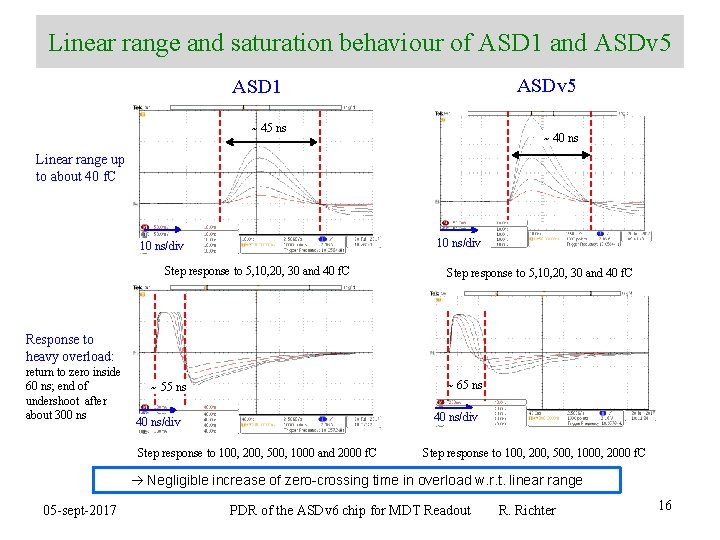
Linear range and saturation behaviour of ASD 1 and ASDv 5 ASD 1 ~ 45 ns ~ 40 ns Linear range up to about 40 f. C 10 ns/div Step response to 5, 10, 20, 30 and 40 f. C Response to heavy overload: return to zero inside 60 ns; end of undershoot after about 300 ns ~ 65 ns ~ 55 ns 40 ns/div Step response to 100, 200, 500, 1000 and 2000 f. C Step response to 100, 200, 500, 1000, 2000 f. C Negligible increase of zero-crossing time in overload w. r. t. linear range 05 -sept-2017 PDR of the ASDv 6 chip for MDT Readout R. Richter 16

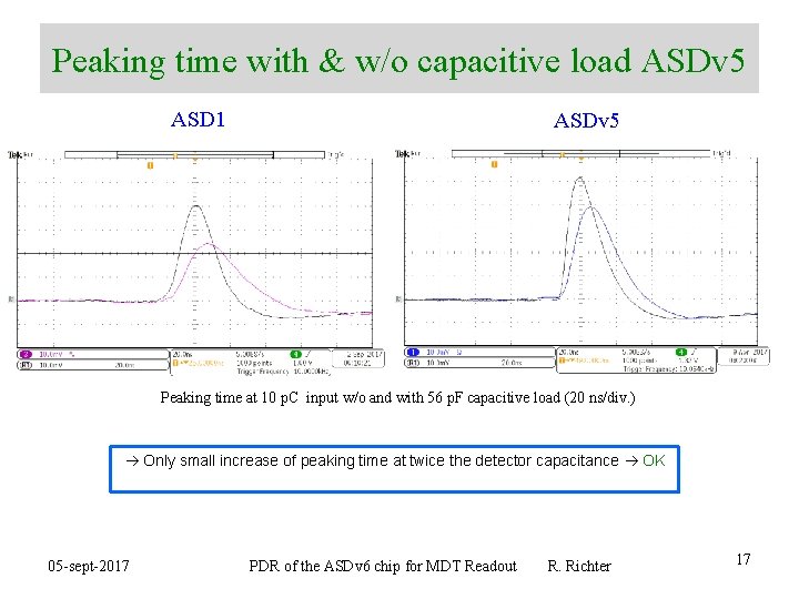
Peaking time with & w/o capacitive load ASDv 5 ASD 1 ASDv 5 Peaking time at 10 p. C input w/o and with 56 p. F capacitive load (20 ns/div. ) Only small increase of peaking time at twice the detector capacitance OK 05 -sept-2017 PDR of the ASDv 6 chip for MDT Readout R. Richter 17

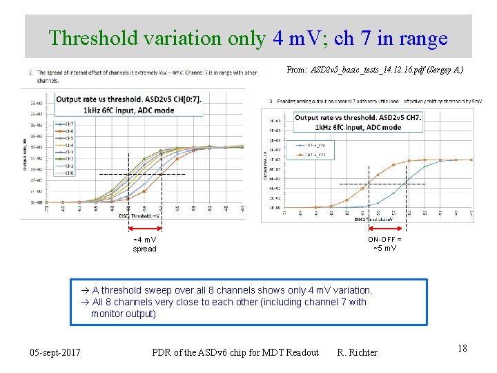
Threshold variation only 4 m. V; ch 7 in range From: ASD 2 v 5_basic_tests_14. 12. 16. pdf (Sergey A. ) ~4 m. V spread ON-OFF = ~5 m. V A threshold sweep over all 8 channels shows only 4 m. V variation. All 8 channels very close to each other (including channel 7 with monitor output) 05 -sept-2017 PDR of the ASDv 6 chip for MDT Readout R. Richter 18

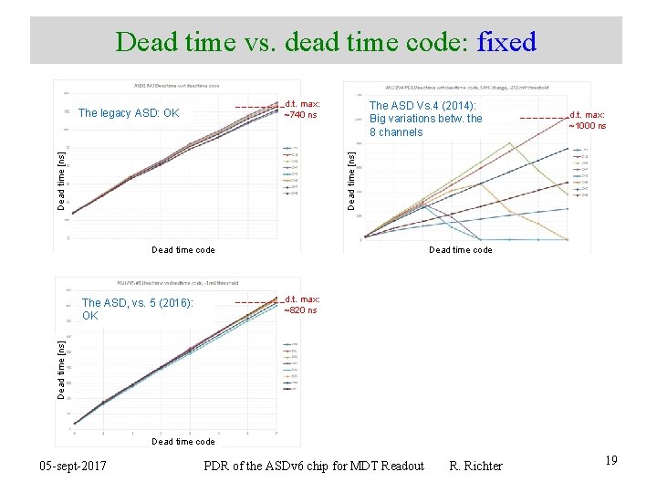
Dead time vs. dead time code: fixed d. t. max: ~740 ns The ASD Vs. 4 (2014): Big variations betw. the 8 channels d. t. max: ~1000 ns Dead time [ns] The legacy ASD: OK Dead time code d. t. max: ~820 ns Dead time [ns] The ASD, vs. 5 (2016): OK Dead time code 05 -sept-2017 PDR of the ASDv 6 chip for MDT Readout R. Richter 19
![ADC vs rundown current code improved Max width 17050 ns ADC pulse widthns ch ADC vs. run-down current code: improved Max. width: 170+-50 ns ADC pulse width[ns] ch](https://slidetodoc.com/presentation_image/164aeec54d94cc37e4dca8c3a204d631/image-20.jpg)
ADC vs. run-down current code: improved Max. width: 170+-50 ns ADC pulse width[ns] ch 0: 400 ns ADC pulse width[ns] ASD vs. 5 (2016): improved, but not perfect ASD vs. 4 (2014): large ch-to-ch spread ch 7: ? ? ? ch 0: 600 ns ch 4: 480 ns Max. width: 230+-50 ns Min. width: 90+-15 ns NEW Min. width: 110+-20 ns OLD Operating point 2: Run-down curr. code 90 -170 ns Run-down curr. code The legacy ASD: significant spread Max. width: 220+-40 ns ASD_Vs. 5 better than Vs. 4, but not OK: For corrections see next talk! ch 0, ch 7: 140+-10 ns Min. width: 90+-10 ns legacy Operating point 2: 100 -150 ns 05 -sept-2017 Run-down curr. code PDR of the ASDv 6 chip for MDT Readout R. Richter 20

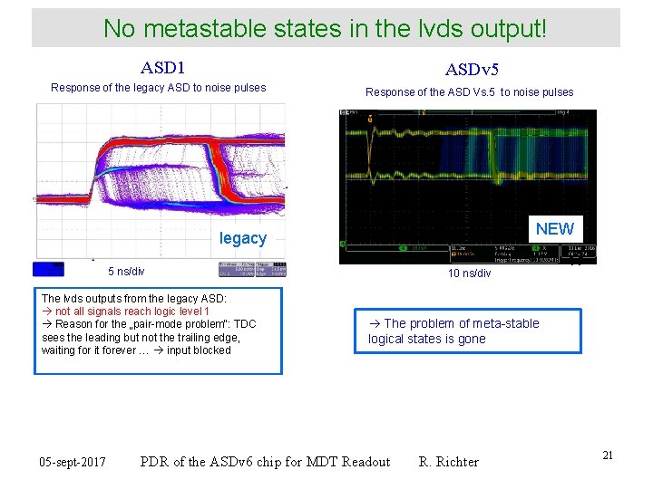
No metastable states in the lvds output! ASD 1 ASDv 5 Response of the legacy ASD to noise pulses Response of the ASD Vs. 5 to noise pulses NEW legacy 5 ns/div The lvds outputs from the legacy ASD: not all signals reach logic level 1 Reason for the „pair-mode problem“: TDC sees the leading but not the trailing edge, waiting for it forever … input blocked 05 -sept-2017 10 ns/div The problem of meta-stable logical states is gone PDR of the ASDv 6 chip for MDT Readout R. Richter 21
![Power consumption vs Vcc Power m W 600 550 500 Power consumption vs. Vcc Power [m. W] • 600 • 550 • 500 •](https://slidetodoc.com/presentation_image/164aeec54d94cc37e4dca8c3a204d631/image-22.jpg)
Power consumption vs. Vcc Power [m. W] • 600 • 550 • 500 • 450 • 400 • 350 • 300 • 250 3 operation points possible • 200 • 150 Infrared photo of ASDv 5 • 100 • 2. 4 • 2. 5 • 2. 6 • 2. 7 • 2. 8 • 2. 9 • 3. 0 • 3. 1 • 3. 2 • 3. 3 • 3. 4 Vcc [V] Further power reduction in analog part and lvds driver under study, to be submitted nov 2017 05 -sept-2017 PDR of the ASDv 6 chip for MDT Readout R. Richter 22
![Peak at Monitor output m V Gain matching between different ASDv 5 chips Input Peak at Monitor output [m. V] Gain matching between different ASDv 5 chips Input](https://slidetodoc.com/presentation_image/164aeec54d94cc37e4dca8c3a204d631/image-23.jpg)
Peak at Monitor output [m. V] Gain matching between different ASDv 5 chips Input charge [f. C] Good gain matching chip-to-chip: Voltage vs. input charge for 2 different chips (channel #7) More info about chip-to-chip matching in S. Abovyan‘s talk 05 -sept-2017 PDR of the ASDv 6 chip for MDT Readout R. Richter 23

ASDv 5: test of the tracking performance a) drift time distribution b) spatial resolution under Phase-II conditions 05 -sept-2017 PDR of the ASDv 6 chip for MDT Readout R. Richter 24

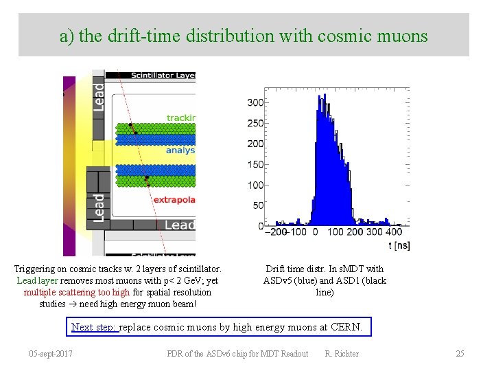
a) the drift-time distribution with cosmic muons Triggering on cosmic tracks w. 2 layers of scintillator. Lead layer removes most muons with p< 2 Ge. V; yet multiple scattering too high for spatial resolution studies need high energy muon beam! Drift time distr. In s. MDT with ASDv 5 (blue) and ASD 1 (black line) Next step: replace cosmic muons by high energy muons at CERN. 05 -sept-2017 PDR of the ASDv 6 chip for MDT Readout R. Richter 25

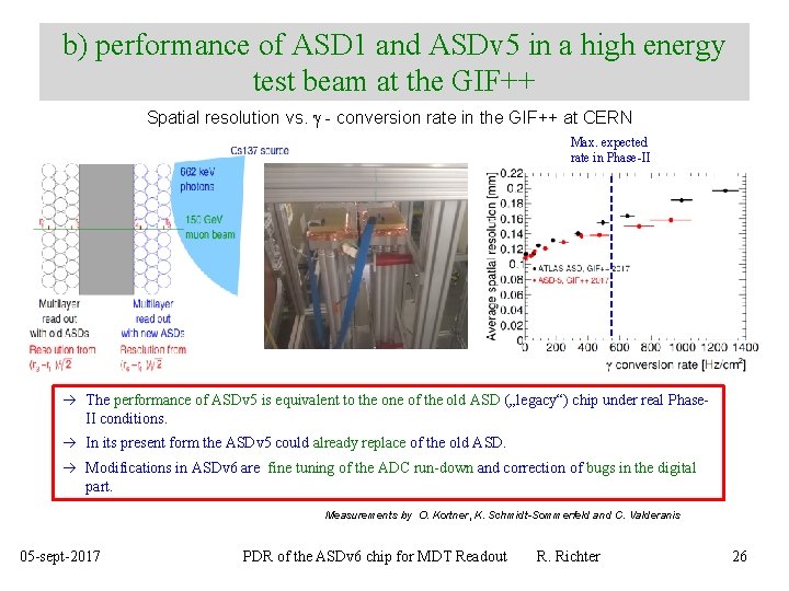
b) performance of ASD 1 and ASDv 5 in a high energy test beam at the GIF++ Spatial resolution vs. g - conversion rate in the GIF++ at CERN Max. expected rate in Phase-II The performance of ASDv 5 is equivalent to the one of the old ASD („legacy“) chip under real Phase. II conditions. In its present form the ASDv 5 could already replace of the old ASD. Modifications in ASDv 6 are fine tuning of the ADC run-down and correction of bugs in the digital part. Measurements by O. Kortner, K. Schmidt-Sommerfeld and C. Valderanis 05 -sept-2017 PDR of the ASDv 6 chip for MDT Readout R. Richter 26

Summary • The ASDv 5 is a chip which can be used for MDT R/O only minor modifications were needed for the aug 2017 submission • Sequence of submissions of ASDv 6 strongly influenced by MPW problem with MOSIS/GF: – ASDv 6, submitted aug 2017, improves control over the run-down current, but minimizing the risk of introducing new errors – 2 variants of ASDv 6 have been submitted, trying to reduce the power of lvds driver – A 3 rd variant will be submitted in nov 2017 to further reduce power consumption in the analog section • The results of the 3 submissions are expected by march 2018 • Measurements show good matching chip-to-chip for gain threshold deadtime etc. (not yet for ADC run-down current …) 05 -sept-2017 PDR of the ASDv 6 chip for MDT Readout R. Richter 27

Backup Slides 05 -sept-2017 PDR of the ASDv 6 chip for MDT Readout R. Richter 28

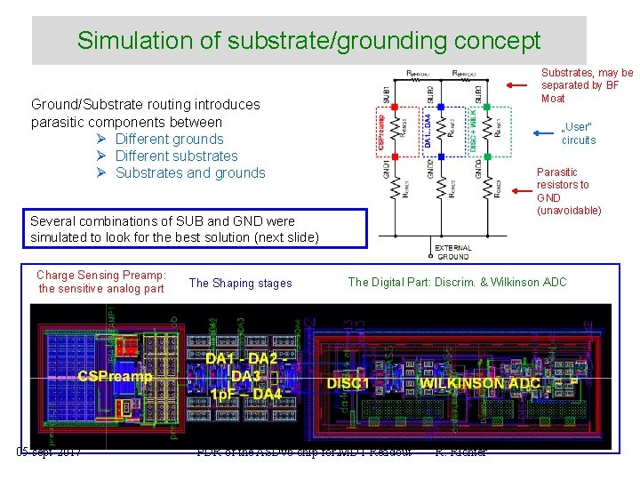
Simulation of substrate/grounding concept Substrates, may be separated by BF Moat Ground/Substrate routing introduces parasitic components between Ø Different grounds Ø Different substrates Ø Substrates and grounds „User“ circuits Parasitic resistors to GND (unavoidable) Several combinations of SUB and GND were simulated to look for the best solution (next slide) Charge Sensing Preamp: the sensitive analog part 05 -sept-2017 The Shaping stages The Digital Part: Discrim. & Wilkinson ADC PDR of the ASDv 6 chip for 29 MDT Readout R. Richter