Power Factor Correction Optimization Options Joel Turchi Agenda







- Slides: 57

Power Factor Correction Optimization Options Joel Turchi

Agenda q Introduction q Upgraded Control Algorithms q Interleaving Channels q The Bridgeless Option q Conclusions 2

Introduction 3

Basic PFC Definitions - Off-line Applications q The mains utility provides a sinusoidal voltage vline(t). q The shape and phase of iline(t) depend on the load. 4

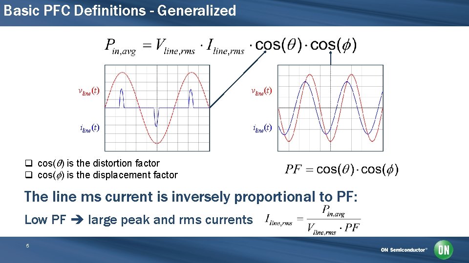
Basic PFC Definitions - Generalized vline(t) iline(t) q cos(q) is the distortion factor q cos(f) is the displacement factor The line ms current is inversely proportional to PF: Low PF large peak and rms currents 5

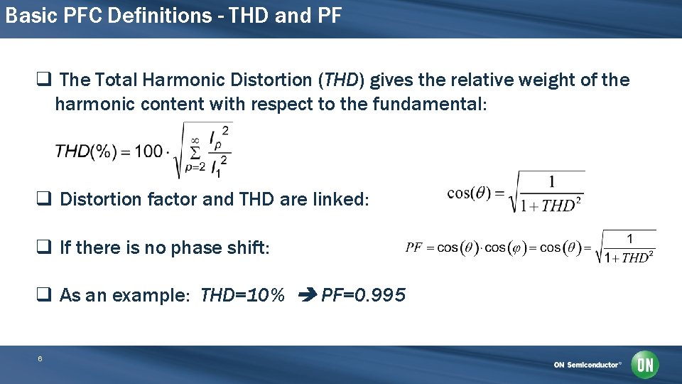
Basic PFC Definitions - THD and PF q The Total Harmonic Distortion (THD) gives the relative weight of the harmonic content with respect to the fundamental: q Distortion factor and THD are linked: q If there is no phase shift: q As an example: THD=10% PF=0. 995 6

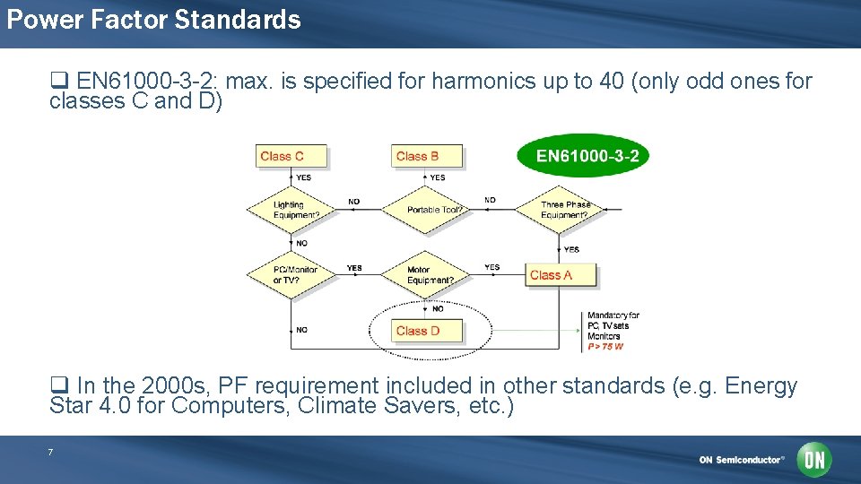
Power Factor Standards q EN 61000 -3 -2: max. is specified for harmonics up to 40 (only odd ones for classes C and D) q In the 2000 s, PF requirement included in other standards (e. g. Energy Star 4. 0 for Computers, Climate Savers, etc. ) 7

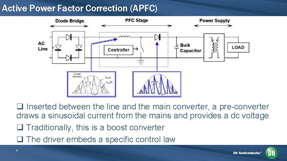
Active Power Factor Correction (APFC) q Inserted between the line and the main converter, a pre-converter draws a sinusoidal current from the mains and provides a dc voltage q Traditionally, this is a boost converter q The driver embeds a specific control law 8

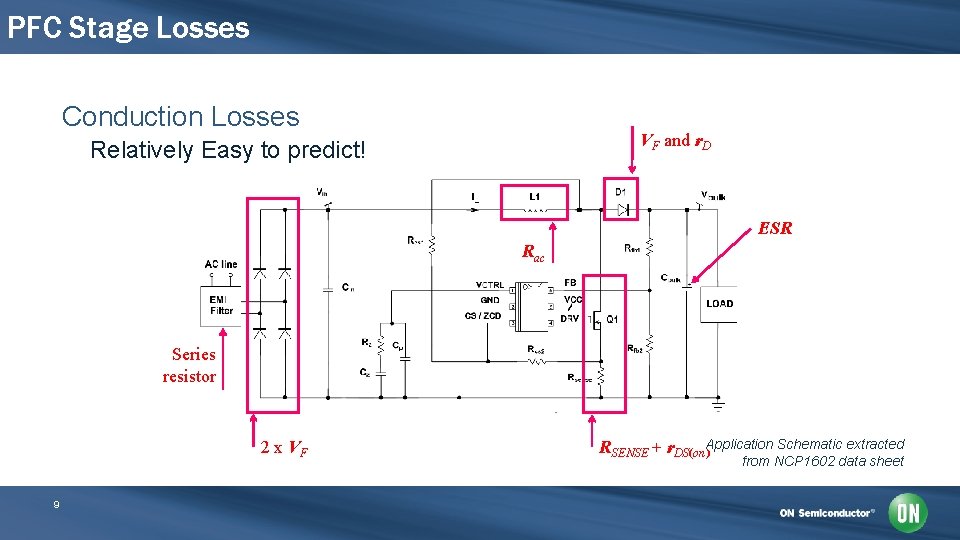
PFC Stage Losses Conduction Losses VF and r. D Relatively Easy to predict! ESR Rac Series resistor 2 x VF 9 RSENSE + r. DS(on)Application Schematic extracted from NCP 1602 data sheet

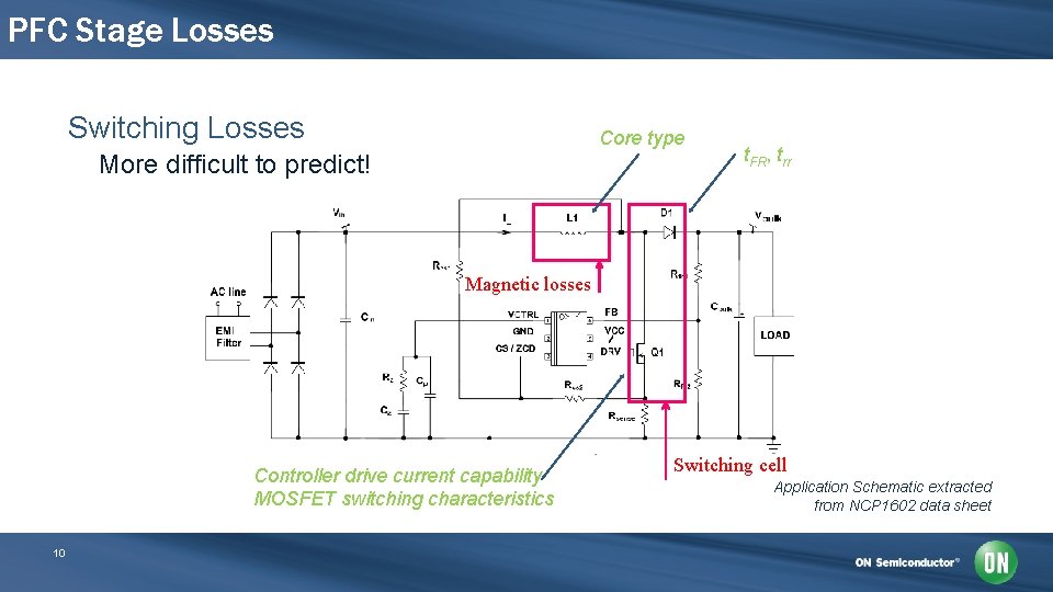
PFC Stage Losses Switching Losses Core type More difficult to predict! t. FR, trr Magnetic losses Controller drive current capability MOSFET switching characteristics 10 Switching cell Application Schematic extracted from NCP 1602 data sheet

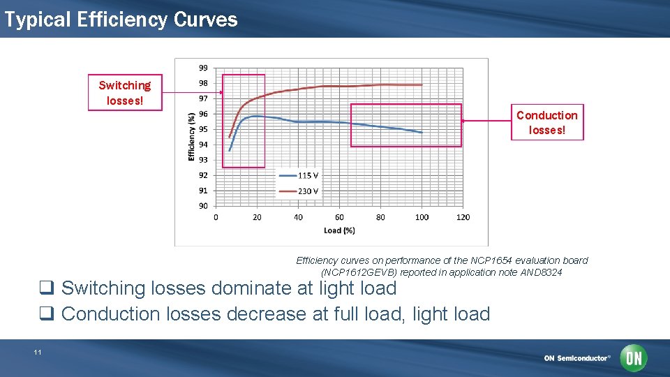
Typical Efficiency Curves Switching losses! Conduction losses! Efficiency curves on performance of the NCP 1654 evaluation board (NCP 1612 GEVB) reported in application note AND 8324 q Switching losses dominate at light load q Conduction losses decrease at full load, light load 11

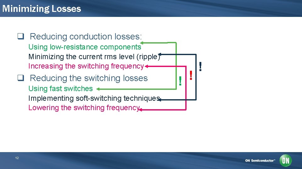
Minimizing Losses q Reducing conduction losses: Using low-resistance components Minimizing the current rms level (ripple) Increasing the switching frequency q Reducing the switching losses Using fast switches Implementing soft-switching techniques Lowering the switching frequency 12 ! ! !

Upgraded Control Algorithms 13

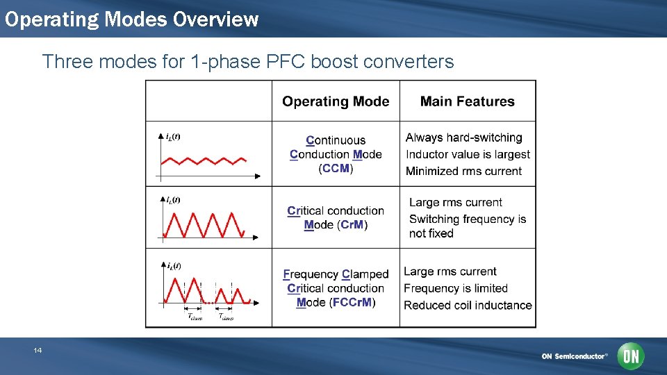
Operating Modes Overview Three modes for 1 -phase PFC boost converters 14

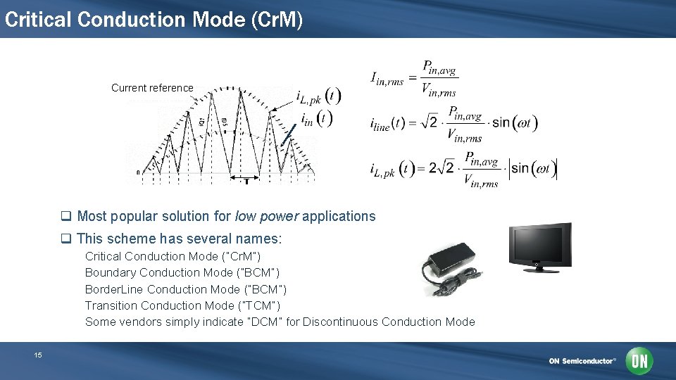
Critical Conduction Mode (Cr. M) Current reference q Most popular solution for low power applications q This scheme has several names: Critical Conduction Mode (“Cr. M”) Boundary Conduction Mode (“BCM”) Border. Line Conduction Mode (“BCM”) Transition Conduction Mode (“TCM”) Some vendors simply indicate “DCM” for Discontinuous Conduction Mode 15

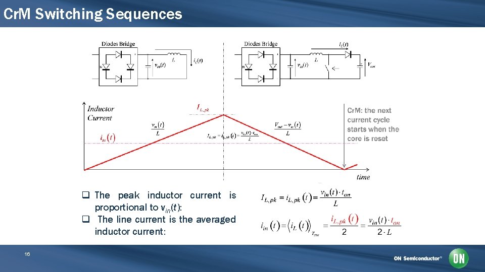
Cr. M Switching Sequences q The peak inductor current is proportional to vin(t): q The line current is the averaged inductor current: 16

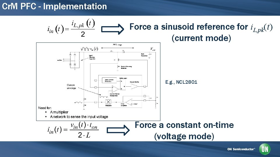
Cr. M PFC - Implementation Force a sinusoid reference for i. L, pk(t) (current mode) E. g. , NCL 2801 Force a constant on-time (voltage mode)

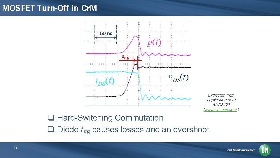
MOSFET Turn-Off in Cr. M 50 ns p(t) t. FR i. DS(t) v. DS(t) Extracted from application note AND 8123 (www. onsemi. com ) q Hard-Switching Commutation q Diode t. FR causes losses and an overshoot 18

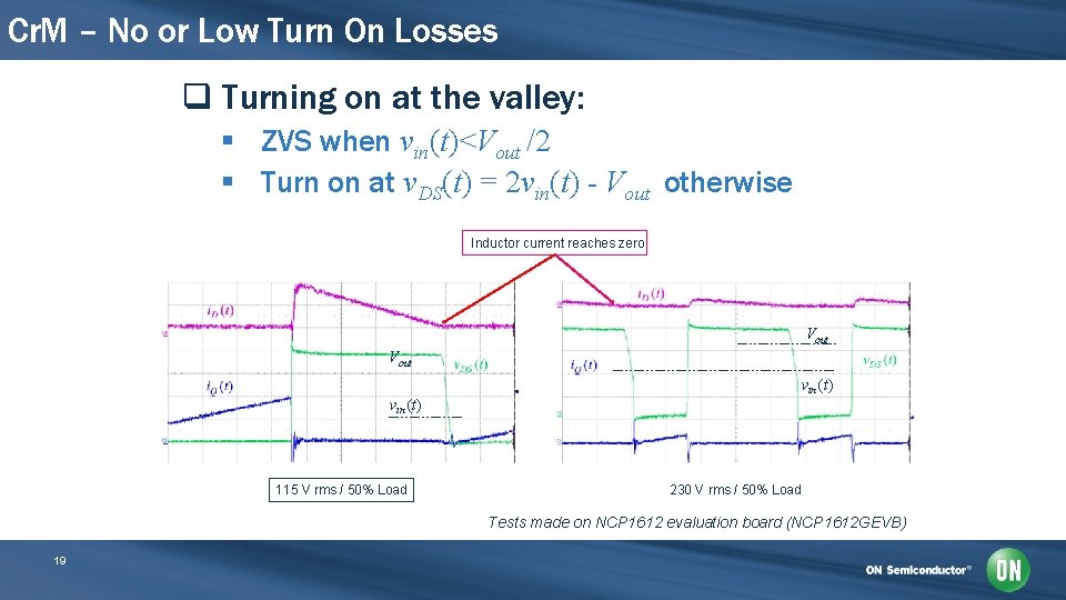
Cr. M – No or Low Turn On Losses q Turning on at the valley: § ZVS when vin(t)<Vout /2 § Turn on at v. DS(t) = 2 vin(t) - Vout otherwise Inductor current reaches zero Vout vin (t) 115 V rms / 50% Load 230 V rms / 50% Load Tests made on NCP 1612 evaluation board (NCP 1612 GEVB) 19

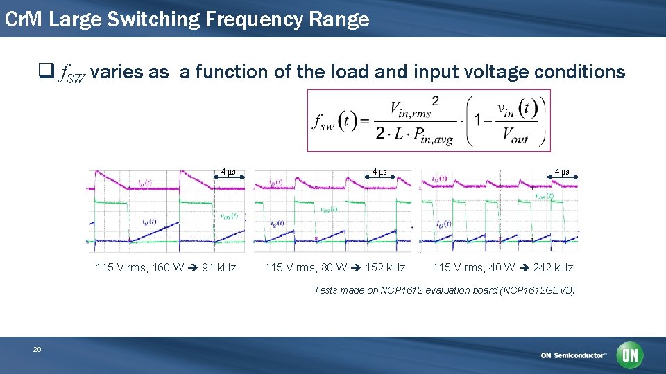
Cr. M Large Switching Frequency Range q f. SW varies as a function of the load and input voltage conditions 4 µs 115 V rms, 160 W 91 k. Hz 4 µs 115 V rms, 80 W 152 k. Hz 4 µs 115 V rms, 40 W 242 k. Hz Tests made on NCP 1612 evaluation board (NCP 1612 GEVB) 20

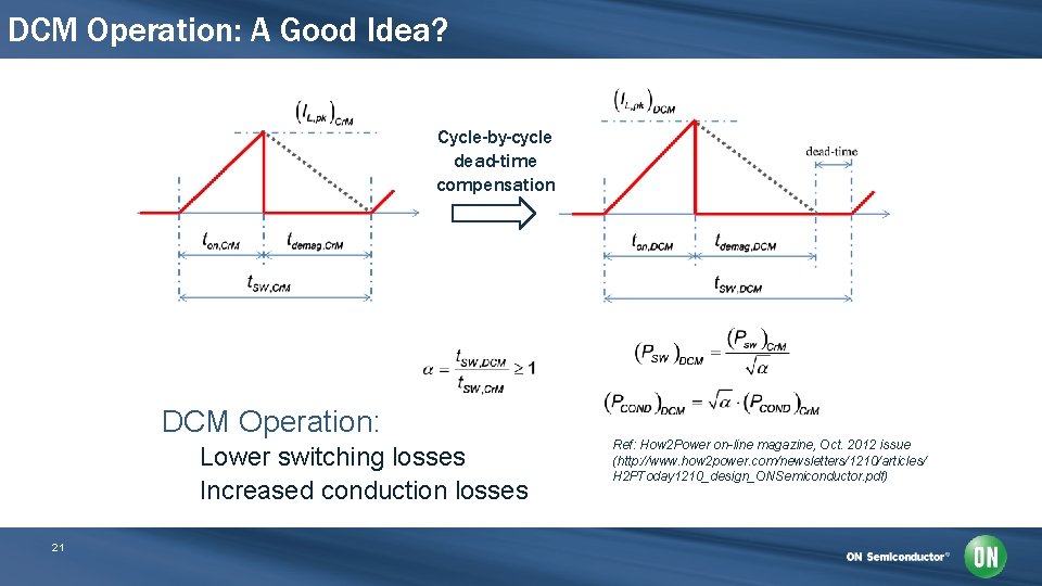
DCM Operation: A Good Idea? Cycle-by-cycle dead-time compensation DCM Operation: Lower switching losses Increased conduction losses 21 Ref: How 2 Power on-line magazine, Oct. 2012 issue (http: //www. how 2 power. com/newsletters/1210/articles/ H 2 PToday 1210_design_ONSemiconductor. pdf)

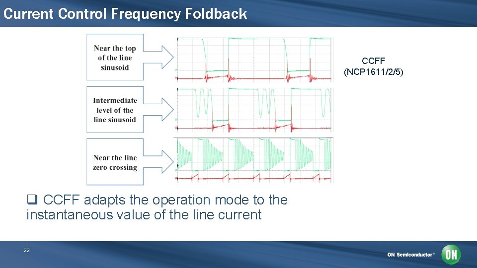
Current Control Frequency Foldback CCFF (NCP 1611/2/5) q CCFF adapts the operation mode to the instantaneous value of the line current 22

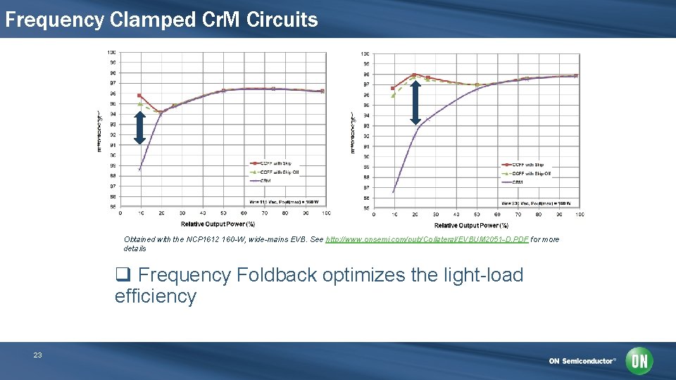
Frequency Clamped Cr. M Circuits Obtained with the NCP 1612 160 -W, wide-mains EVB. See http: //www. onsemi. com/pub/Collateral/EVBUM 2051 -D. PDF for more details q Frequency Foldback optimizes the light-load efficiency 23

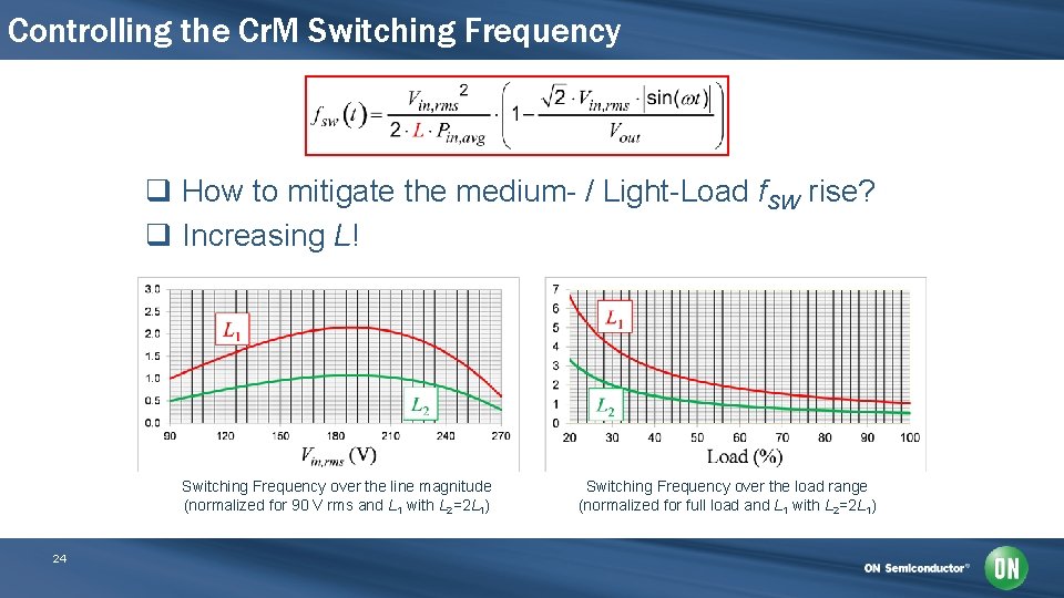
Controlling the Cr. M Switching Frequency q How to mitigate the medium- / Light-Load f. SW rise? q Increasing L! Switching Frequency over the line magnitude (normalized for 90 V rms and L 1 with L 2=2 L 1) 24 Switching Frequency over the load range (normalized for full load and L 1 with L 2=2 L 1)

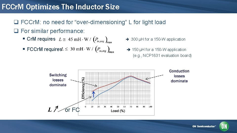
FCCr. M Optimizes The Inductor Size q FCCr. M: no need for “over-dimensioning” L for light load q For similar performance: § Cr. M requires 300 µH for a 150 -W application § FCCr. M requires 150 µH for a 150 -W application (e. g. , NCP 1631 evaluation board) or FC

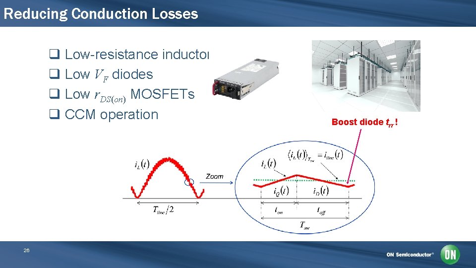
Reducing Conduction Losses q Low-resistance inductors q Low VF diodes q Low r. DS(on) MOSFETs q CCM operation 26 Boost diode trr !

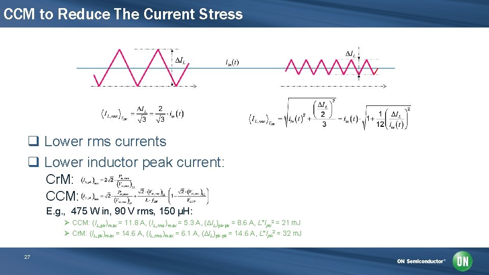
CCM to Reduce The Current Stress q Lower rms currents q Lower inductor peak current: Cr. M: CCM: E. g. , 475 W in, 90 V rms, 150 µH: Ø CCM: (IL, pk)max = 11. 8 A, (IL, rms)max = 5. 3 A, (DIL)pk-pk = 8. 6 A, L*Ipk 2 = 21 m. J Ø Cr. M: (IL, pk)max = 14. 6 A, (IL, rms)max = 6. 1 A, (DIL)pk-pk = 14. 6 A, L*Ipk 2 = 32 m. J 27

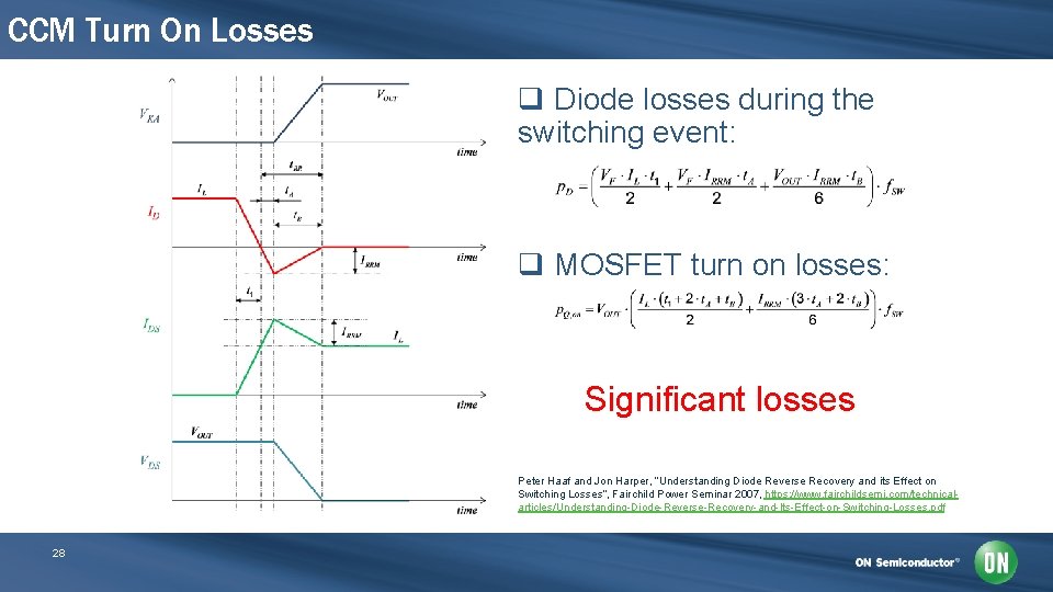
CCM Turn On Losses q Diode losses during the switching event: q MOSFET turn on losses: Significant losses Peter Haaf and Jon Harper, “Understanding Diode Reverse Recovery and its Effect on Switching Losses”, Fairchild Power Seminar 2007, https: //www. fairchildsemi. com/technicalarticles/Understanding-Diode-Reverse-Recovery-and-Its-Effect-on-Switching-Losses. pdf 28

PFC Magnitudes - Computation 29

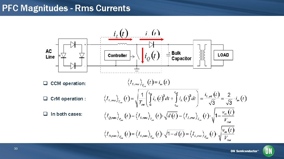
PFC Magnitudes - Rms Currents q CCM operation: q Cr. M operation : q In both cases: 30

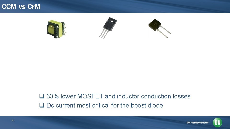
CCM vs Cr. M q 33% lower MOSFET and inductor conduction losses q Dc current most critical for the boost diode 31

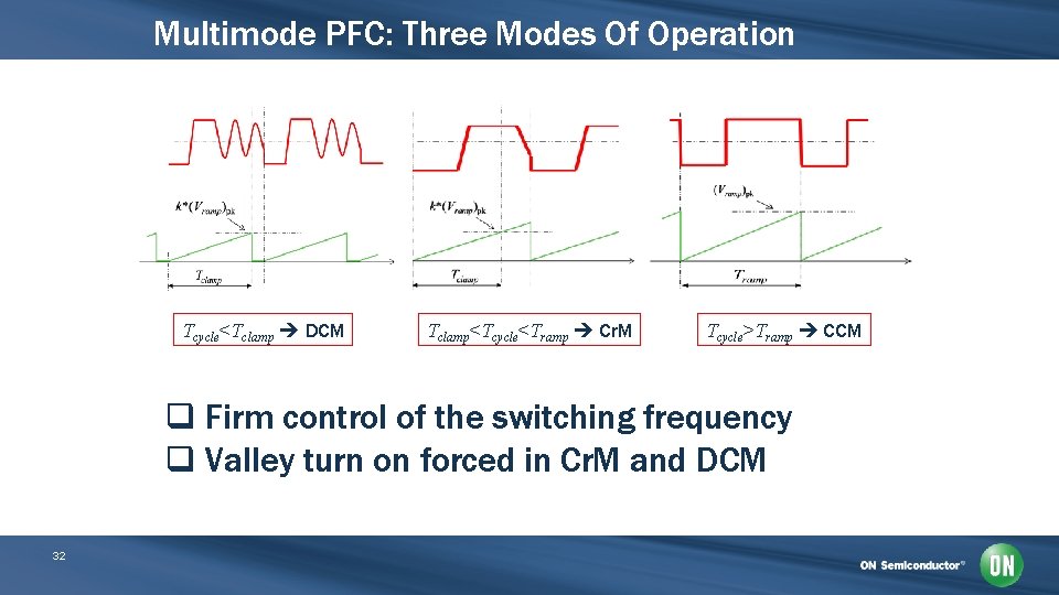
Multimode PFC: Three Modes Of Operation Tcycle<Tclamp DCM Tclamp<Tcycle<Tramp Cr. M Tcycle>Tramp CCM q Firm control of the switching frequency q Valley turn on forced in Cr. M and DCM 32

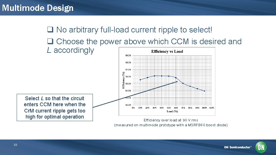
Multimode Design q No arbitrary full-load current ripple to select! q Choose the power above which CCM is desired and L accordingly Select L so that the circuit enters CCM here when the Cr. M current ripple gets too high for optimal operation 33 Efficiency over load at 90 V rms (measured on multimode prototype with a MSRF 860 boost diode)

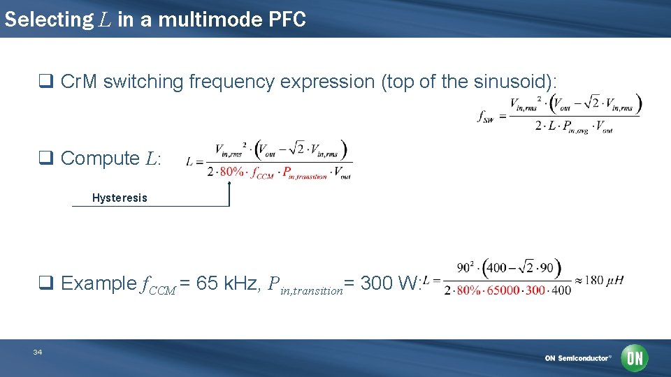
Selecting L in a multimode PFC q Cr. M switching frequency expression (top of the sinusoid): q Compute L: Hysteresis q Example f. CCM = 65 k. Hz, Pin, transition= 300 W: 34

Interleaving Channels 35

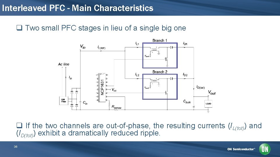
Interleaved PFC - Main Characteristics q Two small PFC stages in lieu of a single big one q If the two channels are out-of-phase, the resulting currents (IL(tot)) and (ID(tot)) exhibit a dramatically reduced ripple. 36

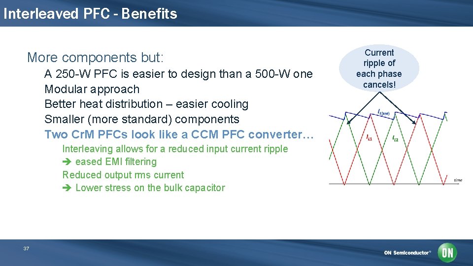
Interleaved PFC - Benefits More components but: A 250 -W PFC is easier to design than a 500 -W one Modular approach Better heat distribution – easier cooling Smaller (more standard) components Two Cr. M PFCs look like a CCM PFC converter… Interleaving allows for a reduced input current ripple eased EMI filtering Reduced output rms current Lower stress on the bulk capacitor 37 Current ripple of each phase cancels!

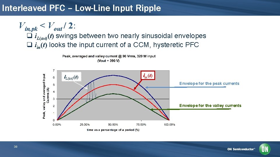
Interleaved PFC – Low-Line Input Ripple Vin, pk < Vout / 2: q i. L(tot)(t) swings between two nearly sinusoidal envelopes q iin(t) looks the input current of a CCM, hysteretic PFC i. L(tot)(t) iin(t) Envelope for the peak currents Envelope for the valley currents 38

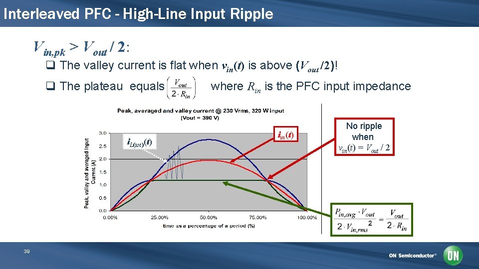
Interleaved PFC - High-Line Input Ripple Vin, pk > Vout / 2: q The valley current is flat when vin(t) is above (Vout / 2)! q The plateau equals where Rin is the PFC input impedance i. L(tot)(t) 39 iin(t) No ripple when vin(t) = Vout / 2

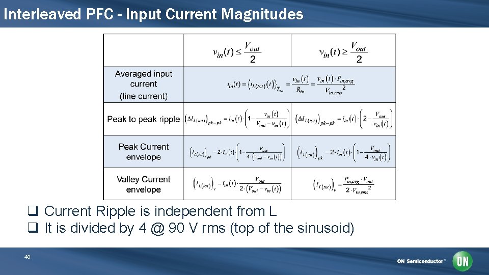
Interleaved PFC - Input Current Magnitudes q Current Ripple is independent from L q It is divided by 4 @ 90 V rms (top of the sinusoid) 40

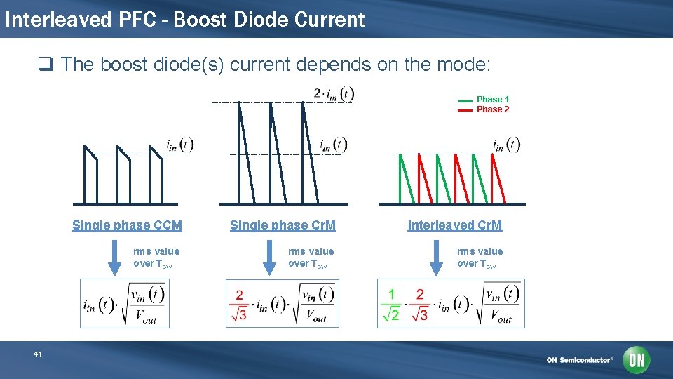
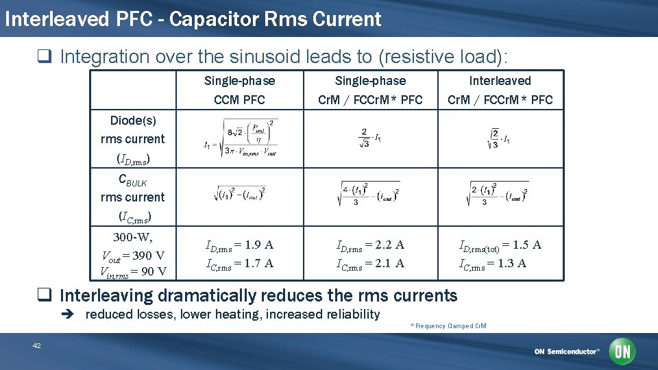
Interleaved PFC - Boost Diode Current q The boost diode(s) current depends on the mode: Phase 1 Phase 2 Single phase CCM rms value over Tsw 41 Single phase Cr. M Interleaved Cr. M rms value over Tsw

Interleaved PFC - Capacitor Rms Current q Integration over the sinusoid leads to (resistive load): Single-phase CCM PFC Single-phase Cr. M / FCCr. M* PFC Interleaved Cr. M / FCCr. M* PFC ID, rms = 1. 9 A IC, rms = 1. 7 A ID, rms = 2. 2 A IC, rms = 2. 1 A ID, rms(tot) = 1. 5 A IC, rms = 1. 3 A Diode(s) rms current (ID, rms) CBULK rms current (IC, rms) 300 -W, Vout = 390 V Vin, rms = 90 V q Interleaving dramatically reduces the rms currents reduced losses, lower heating, increased reliability * Frequency Clamped Cr. M 42

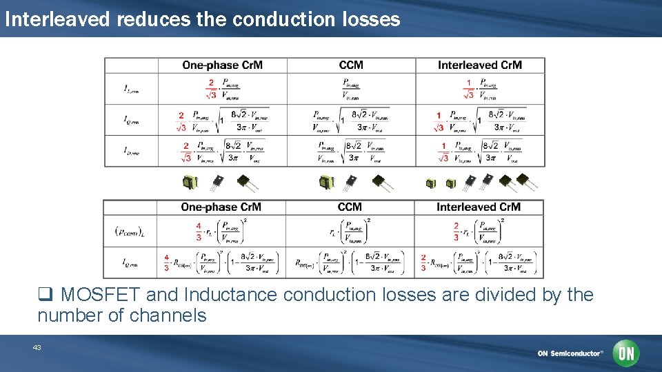
Interleaved reduces the conduction losses q MOSFET and Inductance conduction losses are divided by the number of channels 43

Interleaved Benefits (Cr. M or CCM) q Like if the MOSFET and inductors were simply paralleled, they conduction losses are divided by the number of phase q In addition, the current ripple is dramatically reduced Less EMI filtering required, eased use of low-resistance components Lower magnetic losses q Comparable switching losses compared to single-phase PFC operating in same mode 44

The Bridgeless Option 45

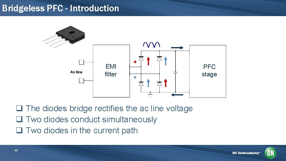
Bridgeless PFC - Introduction EMI filter + + q The diodes bridge rectifies the ac line voltage q Two diodes conduct simultaneously q Two diodes in the current path 46 PFC stage

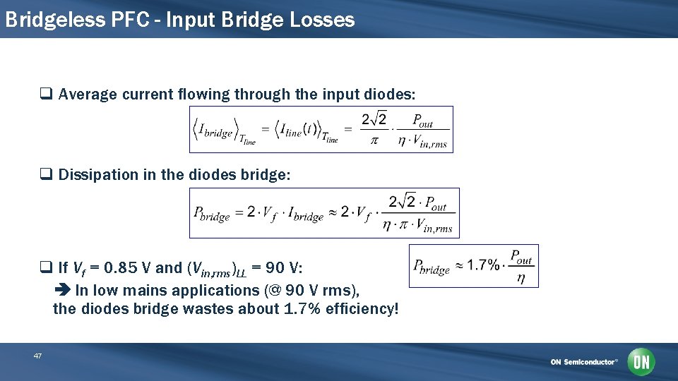
Bridgeless PFC - Input Bridge Losses q Average current flowing through the input diodes: q Dissipation in the diodes bridge: q If Vf = 0. 85 V and (Vin, rms)LL = 90 V: In low mains applications (@ 90 V rms), the diodes bridge wastes about 1. 7% efficiency! 47

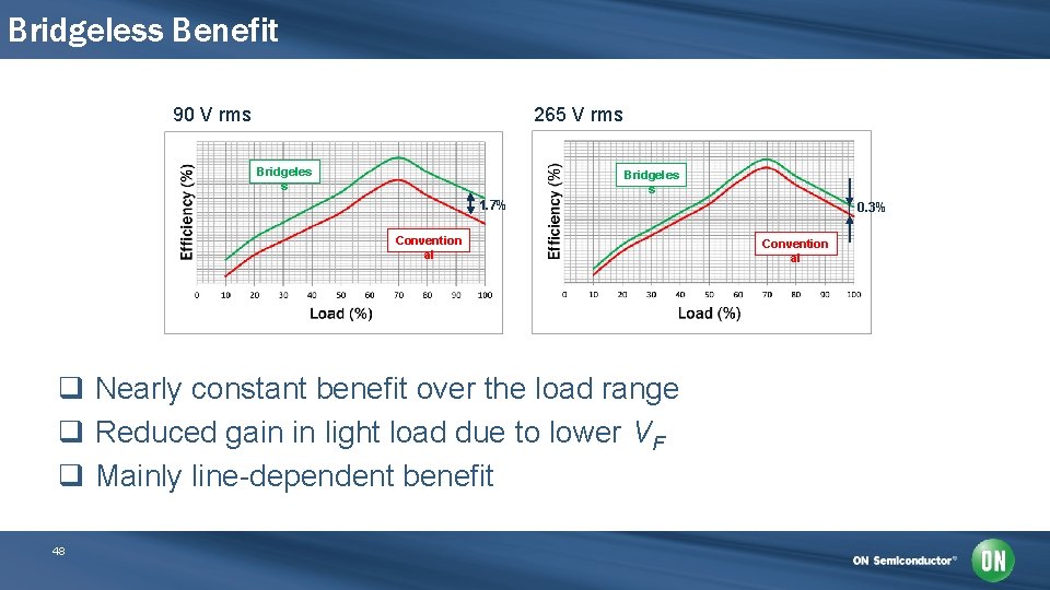
Bridgeless Benefit 90 V rms 265 V rms Bridgeles s 1. 7% Convention al q Nearly constant benefit over the load range q Reduced gain in light load due to lower VF q Mainly line-dependent benefit 48 0. 3% Convention al

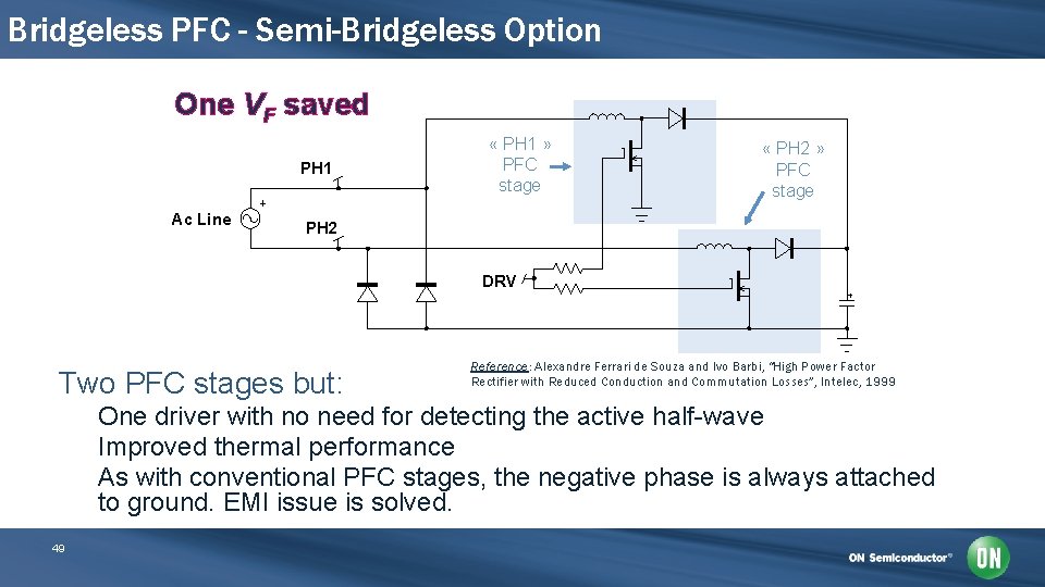
Bridgeless PFC - Semi-Bridgeless Option One VF saved PH 1 Ac Line « PH 1 » PFC stage « PH 2 » PFC stage PH 2 DRV Two PFC stages but: Reference: Alexandre Ferrari de Souza and Ivo Barbi, “High Power Factor Rectifier with Reduced Conduction and Commutation Losses”, Intelec, 1999 One driver with no need for detecting the active half-wave Improved thermal performance As with conventional PFC stages, the negative phase is always attached to ground. EMI issue is solved. 49

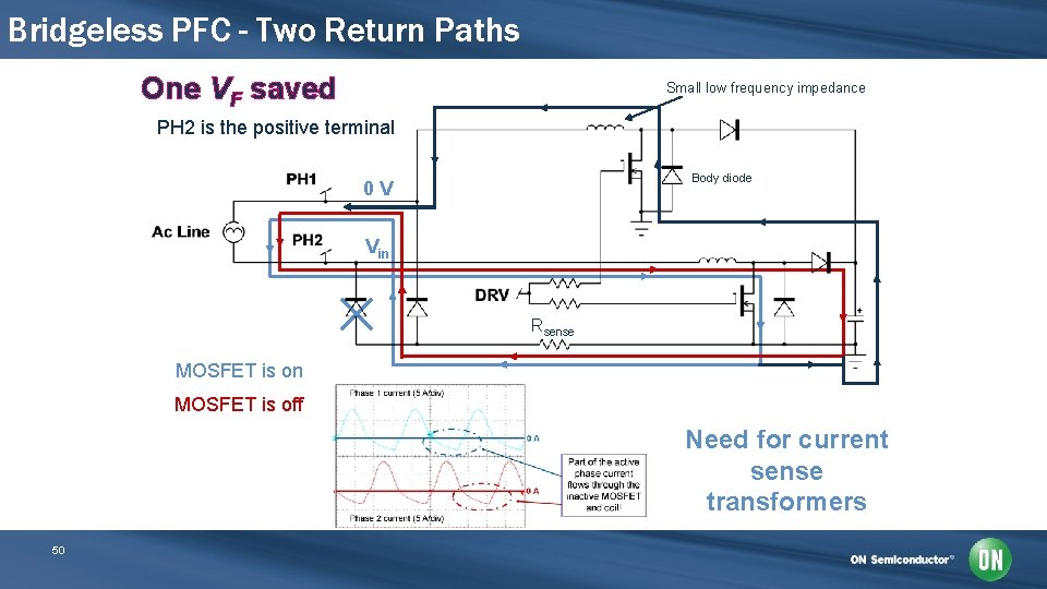
Bridgeless PFC - Two Return Paths One VF saved Small low frequency impedance PH 2 is the positive terminal Body diode 0 V Vin Rsense MOSFET is on MOSFET is off Need for current sense transformers 50

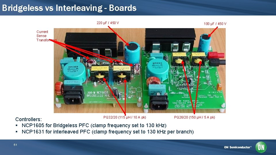
Bridgeless vs Interleaving - Boards 220 µF / 450 V 100 µF / 450 V Current Sense Transformers PQ 32/20 (115 µH / 10 A pk) PQ 26/20 (150 µH / 5 A pk) Controllers: § NCP 1605 for Bridgeless PFC (clamp frequency set to 130 k. Hz) § NCP 1631 for interleaved PFC (clamp frequency set to 130 k. Hz per branch) 51

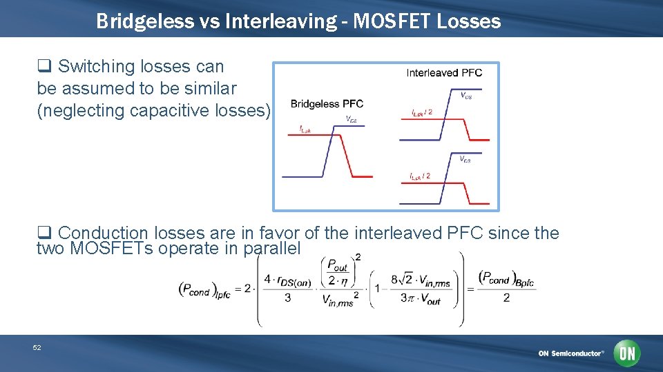
Bridgeless vs Interleaving - MOSFET Losses q Switching losses can be assumed to be similar (neglecting capacitive losses) q Conduction losses are in favor of the interleaved PFC since the two MOSFETs operate in parallel 52

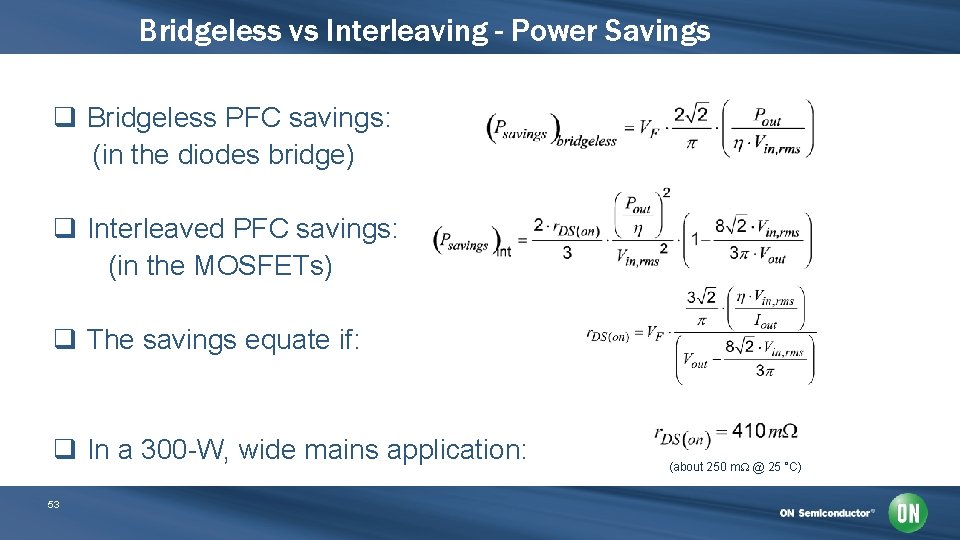
Bridgeless vs Interleaving - Power Savings q Bridgeless PFC savings: (in the diodes bridge) q Interleaved PFC savings: (in the MOSFETs) q The savings equate if: q In a 300 -W, wide mains application: 53 (about 250 m. W @ 25 °C)

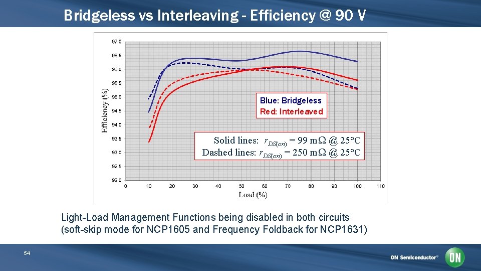
Bridgeless vs Interleaving - Efficiency @ 90 V Blue: Bridgeless Red: Interleaved R = 250 m. W @ 25°C Solid lines: DS(on) r. DS(on) = 99 m. W @ 25°C Dashed lines: r. DS(on) = 250 m. W @ 25°C RDS(on) = 99 m. W @ 25°C Light-Load Management Functions being disabled in both circuits (soft-skip mode for NCP 1605 and Frequency Foldback for NCP 1631) 54

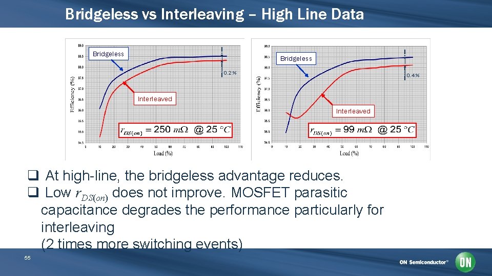
Bridgeless vs Interleaving – High Line Data Bridgeless 0. 2 % 0. 4 % Interleaved q At high-line, the bridgeless advantage reduces. q Low r. DS(on) does not improve. MOSFET parasitic capacitance degrades the performance particularly for interleaving (2 times more switching events) 55

Conclusions 56

Conclusions – Take-Aways q Cr. M is a popular and efficient solution for low power q Components improvements may have increased this power threshold q Frequency reduction techniques necessary for light-load efficiency q Frequency clamp helps optimize the inductor size and cost q Interleaving increases the Cr. M power range by üDramatically reducing the current ripple üReducing the conduction losses q Interleaving requires more components q More compact, CCM is a cost-effective solution for high power q Bridgeless solutions further improve the efficiency at low line but over the whole power range 57