POWER FACTOR CORRECTION Design considerations for optimizing performance


- Slides: 23
POWER FACTOR CORRECTION Design considerations for optimizing performance & cost of continuous mode boost PFC circuits by Supratim Basu, Tore. M. Undeland
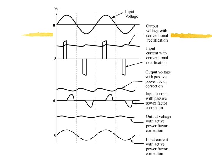
All rectified ac sine wave voltages with capacitive filtering draw high amplitude discontinuous current pulses rich in harmonics , causing: z. Low input power factor z. High circulating currents
There are many approaches to mitigate this problem : z Passive and Active power factor correction z Passive and Active filtering of network z Accepting non-sinusoidal voltage / current in the system.
Passive Power Factor Correction z. Simple inductive input filter z. Inductor stores energy to maintain conduction throughout half cycle z. Hence reduces harmonic distortation and improves power factor z. But size, weight and cost limits it’s application upto 200 W
Active high frequency power factor correction z. Makes load behave like a resistor z. Near unity load power factor z. Load generating negligible harmonics
Types of active PFC circuits with Boost converter topologies z. Hard switched z. Soft switched using ZVT z. Discontinuous Conduction mode (DCM) z. Critical Conduction mode (CRM) z. Continuous Conduction mode (CCM)
Block Diagram of an active PFC Circuit of CCM Boost converter
Mosfet & Diode switching waveforms showing switching losses
Switching loss reduction strategies z. RCD Snubber Circuits z. Magnetic Snubber Circuits z. Power Switch types - IGBT or MOSFET z. Boost Diode Options èSi. C Schottky Diodes èSingle Package Series connected diodes èPFC specific single diodes
RCD Snubber Circuits
Magnetic Snubber Circuit
Comparison of recovery time of various diodes
Comparision of RECOVERY TIME and COST of various diodes
Experimental Results
Effect of Diode Recovery Current on the Switching Current at turn-on The switch turn-on peak current was the lowest for the Si. C Schottky Diode and highest for the Single Package Series Diode
Effect of Diode recovery current on Mosfet drain current with a Si. C Diode
Effect of Diode recovery current on Mosfet drain current with a PFC specific diode
Effect of Diode recovery current on Mosfet drain current with a single package series connected diode
Conducted EMI generated by the PFC board was measured separately for each of the three diode types: z Measurements were made at 90 V AC input, 600 W output load with a 3 m. H common mode EMI filter connected at the input circuit è Low freq part of conducted emission spectrum ( 150 k. Hz - 1 MHz) is almost unaffected by different diode types è High freq part of conducted emission spectrum ( 1 MHz 30 MHz) is affected by diode behavior u SDT 12 S 60 u Increased Si. C Schottky diode generates lower noise EMI caused by STTH 806 TTI single package series connected diodes is only about 4 d. B V
Low frequency conducted emission Single package series connected diode Si. C Diode PFC Specific Diode
High frequency conducted emission Si. C Diode Single package series connected diode PFC Specific Diode
OPTIMIZING PERFORMANCE BY DESIGN A SUMMARY z Power levels < 200 W - Critical conduction mode PFC may be considered z Power levels > 200 W - Hard switched CCM PFC is preferred z Power levels < 1000 W & sw. freq of 100 k. Hz - PFC specific is the best choice z Power levels > 1000 W & sw. freq > 100 k. Hz - Higher initial costs of Si. C Schottky diodes are justified z Higher efficiency or higher sw. freq - ZVT resonant mode boost converter may be considered z Power levels < 600 W - Older generation Mosfets like IRF 460 N(IR) could reduce costs w/o affecting performance significantly