Overview Finite State Machines Sequential circuits with inputs
![Memory Design – 1 K x 4 A[09: 00] Addr Block Select D[03: 00] Memory Design – 1 K x 4 A[09: 00] Addr Block Select D[03: 00]](https://slidetodoc.com/presentation_image_h2/3389e77eb628761e3393fc8887d9e67b/image-26.jpg)
![Memory Design – 1 K x 8 D[07: 04] D[03: 00] A[09: 00] D[07: Memory Design – 1 K x 8 D[07: 04] D[03: 00] A[09: 00] D[07:](https://slidetodoc.com/presentation_image_h2/3389e77eb628761e3393fc8887d9e67b/image-27.jpg)
![Memory Design - 2 k x 8 D[07: 04] Block 01 Block 00 D[03: Memory Design - 2 k x 8 D[07: 04] Block 01 Block 00 D[03:](https://slidetodoc.com/presentation_image_h2/3389e77eb628761e3393fc8887d9e67b/image-28.jpg)
![Memory Design - 4 k x 8 D[07: 04] Block 11 Block 10 Block Memory Design - 4 k x 8 D[07: 04] Block 11 Block 10 Block](https://slidetodoc.com/presentation_image_h2/3389e77eb628761e3393fc8887d9e67b/image-29.jpg)
- Slides: 29

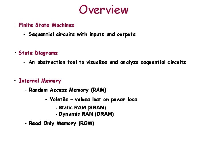
Overview • Finite State Machines - Sequential circuits with inputs and outputs • State Diagrams - An abstraction tool to visualize and analyze sequential circuits • Internal Memory - Random Access Memory (RAM) - Volatile – values lost on power loss - Static RAM (SRAM) - Dynamic RAM (DRAM) - Read Only Memory (ROM)

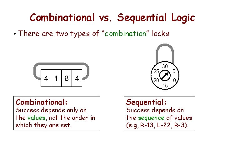
Combinational vs. Sequential Logic • There are two types of “combination” locks 25 4 1 8 4 Combinational: Success depends only on the values, not the order in which they are set. 20 30 15 Sequential: 5 10 Success depends on the sequence of values (e. g, R-13, L-22, R-3).

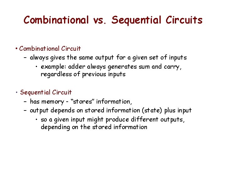
Combinational vs. Sequential Circuits • Combinational Circuit – always gives the same output for a given set of inputs • example: adder always generates sum and carry, regardless of previous inputs • Sequential Circuit – has memory - “stores” information, – output depends on stored information (state) plus input • so a given input might produce different outputs, depending on the stored information

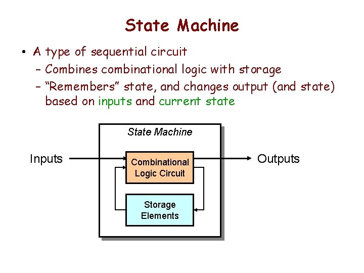
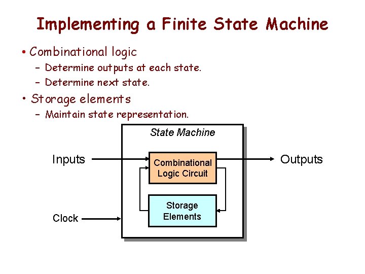
State Machine • A type of sequential circuit – Combines combinational logic with storage – “Remembers” state, and changes output (and state) based on inputs and current state State Machine Inputs Combinational Logic Circuit Storage Elements Outputs

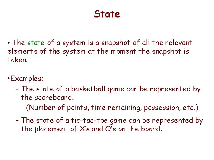
State • The state of a system is a snapshot of all the relevant elements of the system at the moment the snapshot is taken. • Examples: – The state of a basketball game can be represented by the scoreboard. (Number of points, time remaining, possession, etc. ) – The state of a tic-tac-toe game can be represented by the placement of X’s and O’s on the board.

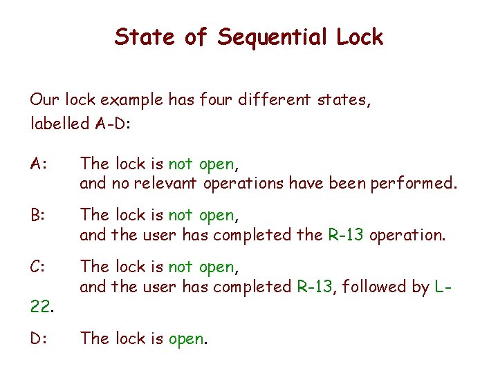
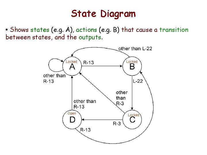
State of Sequential Lock Our lock example has four different states, labelled A-D: A: The lock is not open, and no relevant operations have been performed. B: The lock is not open, and the user has completed the R-13 operation. C: The lock is not open, and the user has completed R-13, followed by L- 22. D: The lock is open.

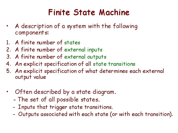
Finite State Machine • A description of a system with the following components: 1. 2. 3. 4. 5. A finite number of states A finite number of external inputs A finite number of external outputs An explicit specification of all state transitions An explicit specification of what determines each external output value • Often described by a state diagram. - The set of all possible states. - Inputs that trigger state transitions. - Outputs associated with each state (or with each transition).

State Diagram • Shows states (e. g. A), actions (e. g. B) that cause a transition between states, and the outputs. Locked Open Locked

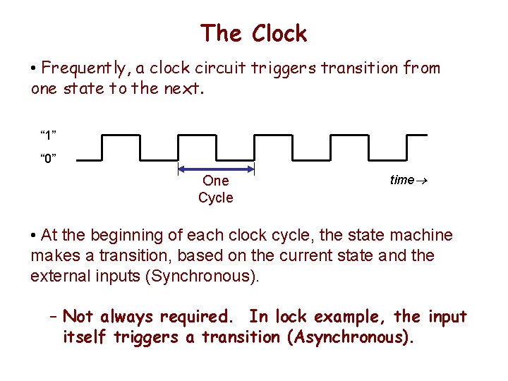
The Clock • Frequently, a clock circuit triggers transition from one state to the next. “ 1” “ 0” One Cycle time • At the beginning of each clock cycle, the state machine makes a transition, based on the current state and the external inputs (Synchronous). – Not always required. In lock example, the input itself triggers a transition (Asynchronous).

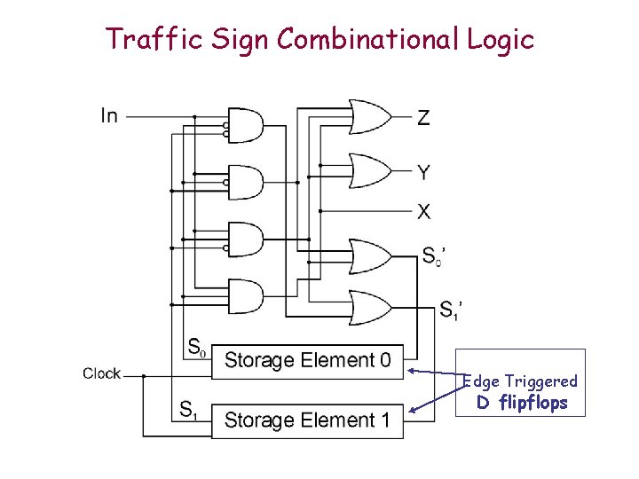
Implementing a Finite State Machine • Combinational logic – Determine outputs at each state. – Determine next state. • Storage elements – Maintain state representation. State Machine Inputs Clock Combinational Logic Circuit Storage Elements Outputs

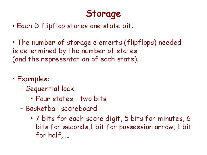
Storage • Each D flipflop stores one state bit. • The number of storage elements (flipflops) needed is determined by the number of states (and the representation of each state). • Examples: – Sequential lock • Four states – two bits – Basketball scoreboard • 7 bits for each score digit, 5 bits for minutes, 6 bits for seconds, 1 bit for possession arrow, 1 bit for half, …

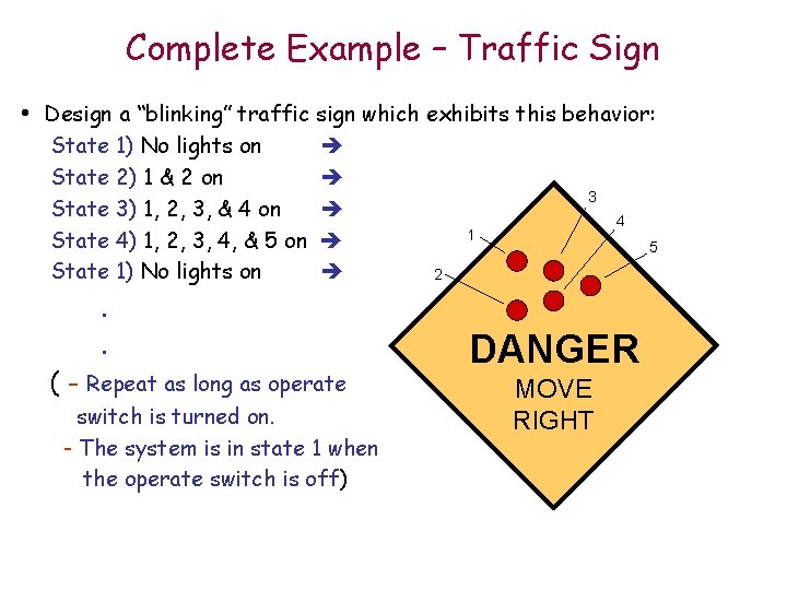
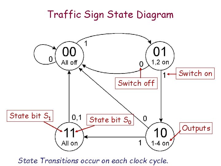
Complete Example – Traffic Sign • Design a “blinking” traffic sign which exhibits this behavior: State 1) No lights on State 2) 1 & 2 on State 3) 1, 2, 3, & 4 on State 4) 1, 2, 3, 4, & 5 on State 1) No lights on . . ( - Repeat as long as operate switch is turned on. - The system is in state 1 when the operate switch is off) 3 4 1 5 2 DANGER MOVE RIGHT

Traffic Sign State Diagram Switch off State bit S 1 State bit S 0 State Transitions occur on each clock cycle. Switch on Outputs

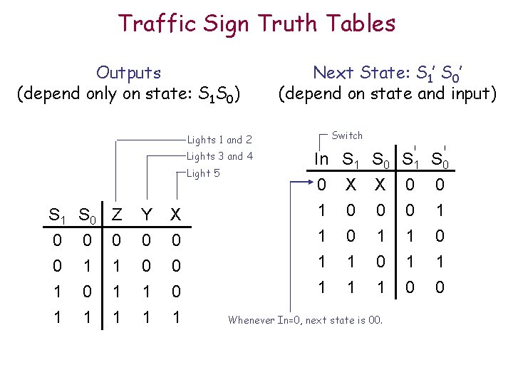
Traffic Sign Truth Tables Outputs (depend only on state: S 1 S 0) Next State: S 1’ S 0’ (depend on state and input) Switch Lights 1 and 2 Lights 3 and 4 Light 5 S 1 0 0 1 S 0 0 1 0 Z 0 1 1 Y 0 0 1 X 0 0 0 1 1 1 In S 1 0 X 1 0 S 0 X 0 1 S 1 0 0 1 S 0 0 1 1 0 1 0 1 1 Whenever In=0, next state is 00.

Traffic Sign Combinational Logic Edge Triggered D flipflops

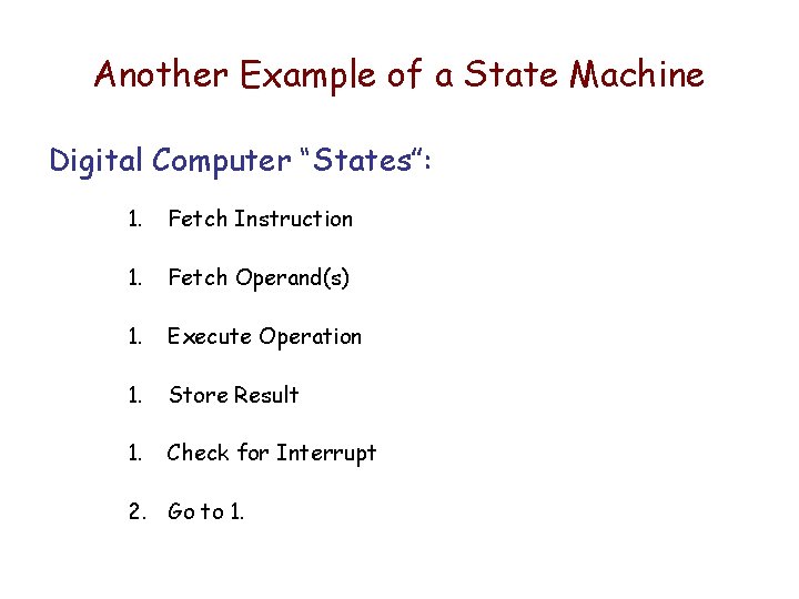
Another Example of a State Machine Digital Computer “States”: 1. Fetch Instruction 1. Fetch Operand(s) 1. Execute Operation 1. Store Result 1. Check for Interrupt 2. Go to 1.

Computer Memory

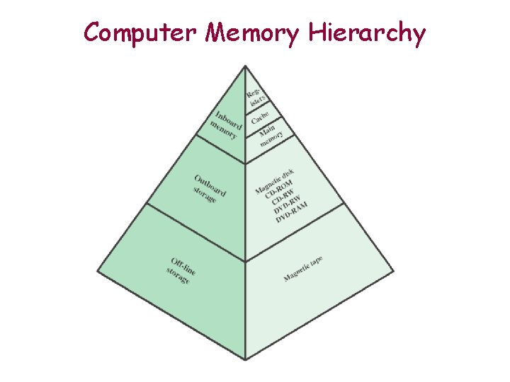
Computer Memory Hierarchy

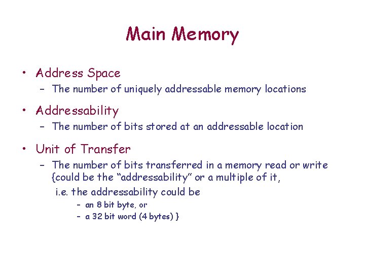
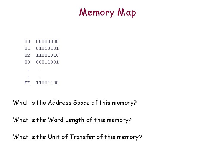
Main Memory • Address Space – The number of uniquely addressable memory locations • Addressability – The number of bits stored at an addressable location • Unit of Transfer – The number of bits transferred in a memory read or write {could be the “addressability” or a multiple of it, i. e. the addressability could be – an 8 bit byte, or – a 32 bit word (4 bytes) }

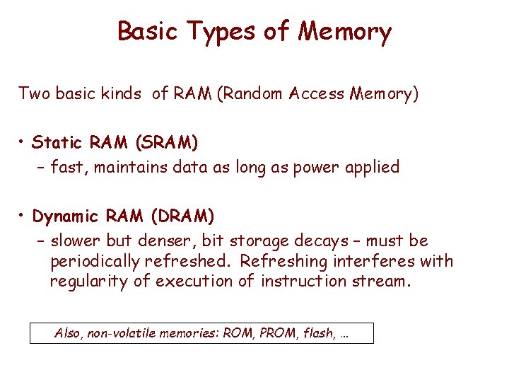
Basic Types of Memory Two basic kinds of RAM (Random Access Memory) • Static RAM (SRAM) – fast, maintains data as long as power applied • Dynamic RAM (DRAM) – slower but denser, bit storage decays – must be periodically refreshed. Refreshing interferes with regularity of execution of instruction stream. Also, non-volatile memories: ROM, PROM, flash, …

Memory Map 00 01 02 03. . FF 0000 0101 11001010 00011001. . 1100 What is the Address Space of this memory? What is the Word Length of this memory? What is the Unit of Transfer of this memory?

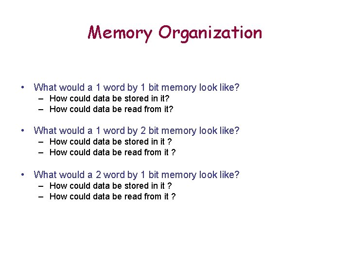
Memory Organization • What would a 1 word by 1 bit memory look like? – How could data be stored in it? – How could data be read from it? • What would a 1 word by 2 bit memory look like? – How could data be stored in it ? – How could data be read from it ? • What would a 2 word by 1 bit memory look like? – How could data be stored in it ? – How could data be read from it ?

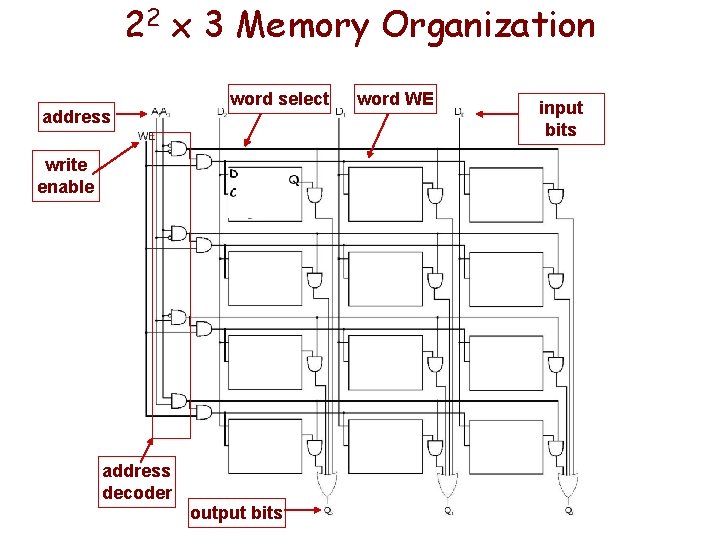
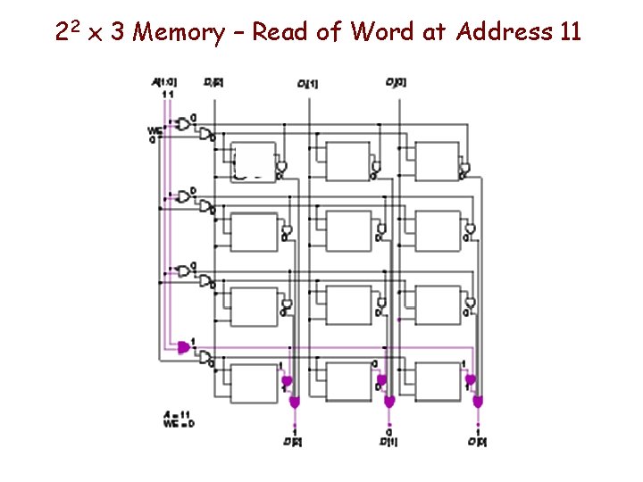
22 x 3 Memory Organization address word select write enable address decoder output bits word WE input bits

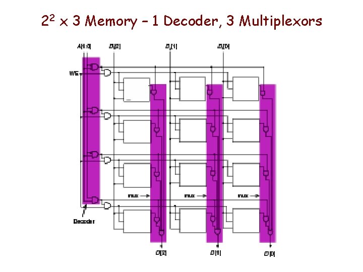
22 x 3 Memory – 1 Decoder, 3 Multiplexors

22 x 3 Memory – Read of Word at Address 11
![Memory Design 1 K x 4 A09 00 Addr Block Select D03 00 Memory Design – 1 K x 4 A[09: 00] Addr Block Select D[03: 00]](https://slidetodoc.com/presentation_image_h2/3389e77eb628761e3393fc8887d9e67b/image-26.jpg)
Memory Design – 1 K x 4 A[09: 00] Addr Block Select D[03: 00]
![Memory Design 1 K x 8 D07 04 D03 00 A09 00 D07 Memory Design – 1 K x 8 D[07: 04] D[03: 00] A[09: 00] D[07:](https://slidetodoc.com/presentation_image_h2/3389e77eb628761e3393fc8887d9e67b/image-27.jpg)
Memory Design – 1 K x 8 D[07: 04] D[03: 00] A[09: 00] D[07: 04] Addr Block Select => D[03: 00] Addr Block Select =>
![Memory Design 2 k x 8 D07 04 Block 01 Block 00 D03 Memory Design - 2 k x 8 D[07: 04] Block 01 Block 00 D[03:](https://slidetodoc.com/presentation_image_h2/3389e77eb628761e3393fc8887d9e67b/image-28.jpg)
Memory Design - 2 k x 8 D[07: 04] Block 01 Block 00 D[03: 00]
![Memory Design 4 k x 8 D07 04 Block 11 Block 10 Block Memory Design - 4 k x 8 D[07: 04] Block 11 Block 10 Block](https://slidetodoc.com/presentation_image_h2/3389e77eb628761e3393fc8887d9e67b/image-29.jpg)
Memory Design - 4 k x 8 D[07: 04] Block 11 Block 10 Block 01 Block 00 D[03: 00]