Memory Sequential Clocked Circuits Finite State Machines COS
- Slides: 28

Memory; Sequential & Clocked Circuits; Finite State Machines COS 116: 3/25/2008 Sanjeev Arora

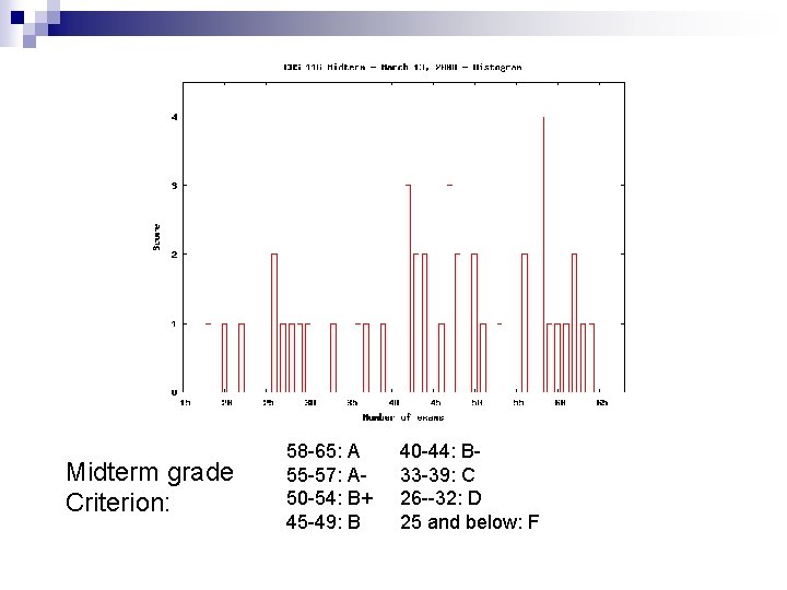
Midterm grade Criterion: 58 -65: A 55 -57: A 50 -54: B+ 45 -49: B 40 -44: B 33 -39: C 26 --32: D 25 and below: F

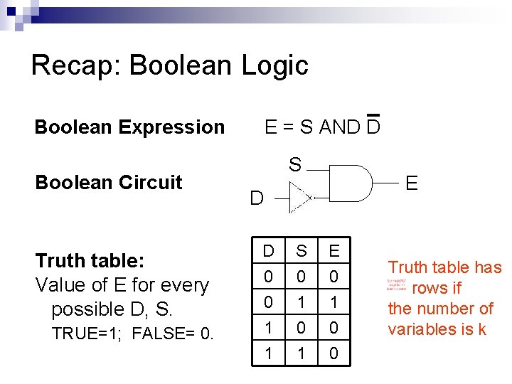
Recap: Boolean Logic Boolean Expression Boolean Circuit Truth table: Value of E for every possible D, S. TRUE=1; FALSE= 0. E = S AND D S E D D 0 S 0 E 0 0 1 1 1 0 0 1 1 0 Truth table has rows if the number of variables is k

Boole’s reworking of Clarke’s “proof” of existence of God (see handout) n General idea: Try to prove that Boolean expressions E 1, E 2, …, Ek cannot simultaneously be true n Method: Show E 1· E 2 · … · Ek = 0 n Discussion: What exactly does Clarke’s “proof” prove? How convincing is such a proof to you? Also: Do Google search for “Proof of God’s Existence. ”

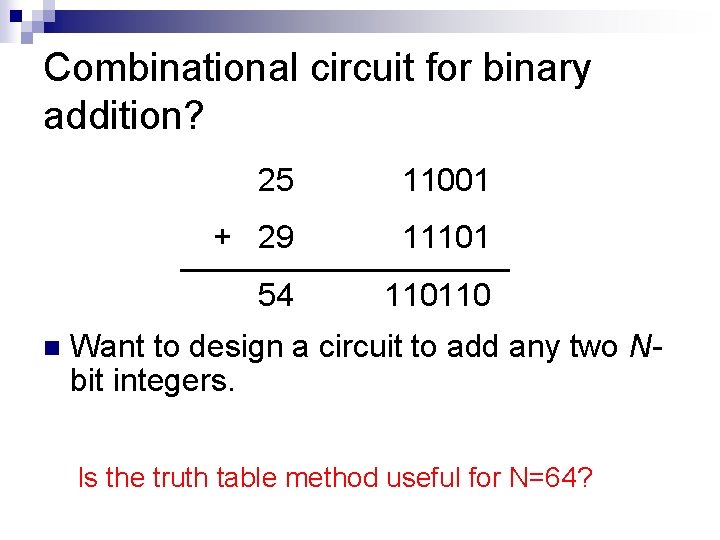
Combinational circuit for binary addition? n 25 11001 + 29 11101 54 110110 Want to design a circuit to add any two Nbit integers. Is the truth table method useful for N=64?

Modular design Have small number of basic components. Put them together to achieve desired functionality Basic principle of modern industrial design; recurring theme in next few lectures.

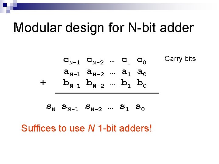
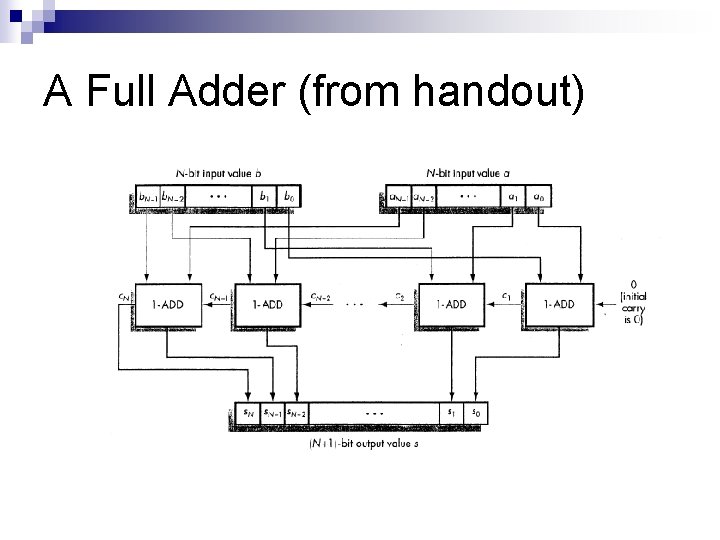
Modular design for N-bit adder + c. N-1 c. N-2 … c 1 c 0 a. N-1 a. N-2 … a 1 a 0 b. N-1 b. N-2 … b 1 b 0 s. N-1 s. N-2 … s 1 s 0 Suffices to use N 1 -bit adders! Carry bits

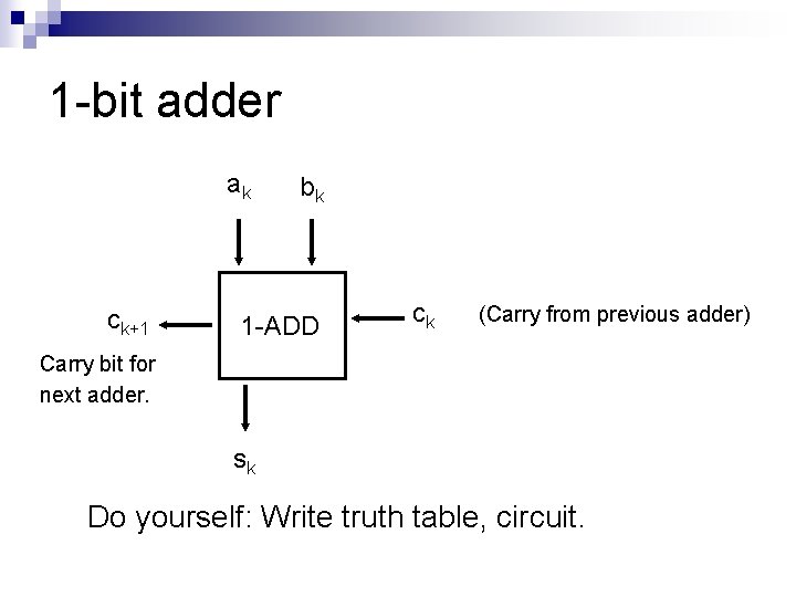
1 -bit adder ak ck+1 bk 1 -ADD ck (Carry from previous adder) Carry bit for next adder. sk Do yourself: Write truth table, circuit.

A Full Adder (from handout)

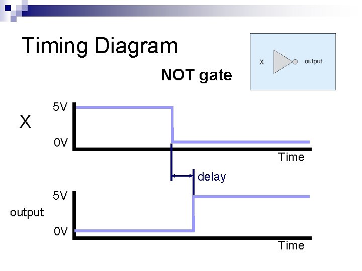
Timing Diagram NOT gate X 5 V 0 V Time delay 5 V output 0 V Time

Memory Rest of this lecture: How boolean circuits can have “memory”.

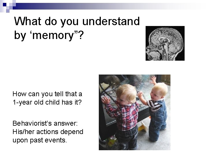
What do you understand by ‘memory”? How can you tell that a 1 -year old child has it? Behaviorist’s answer: His/her actions depend upon past events.

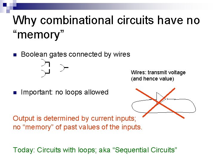
Why combinational circuits have no “memory” n Boolean gates connected by wires Wires: transmit voltage (and hence value) n Important: no loops allowed Output is determined by current inputs; no “memory” of past values of the inputs. Today: Circuits with loops; aka “Sequential Circuits”

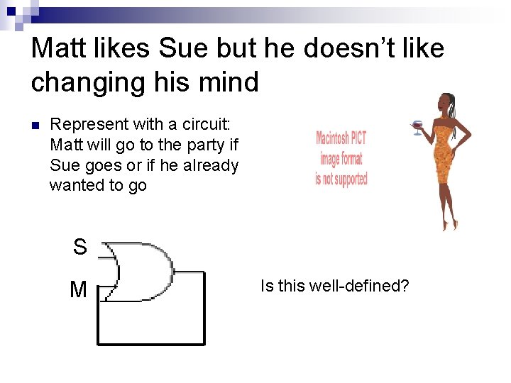
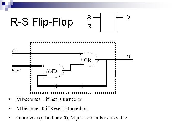
Matt likes Sue but he doesn’t like changing his mind n Represent with a circuit: Matt will go to the party if Sue goes or if he already wanted to go S M Is this well-defined?

Sequential Circuits n Circuits with AND, OR and NOT gates. n Cycles are allowed (ie outputs can feed back into inputs) n Can exhibit “memory”. n Sometimes may have “undefined” values

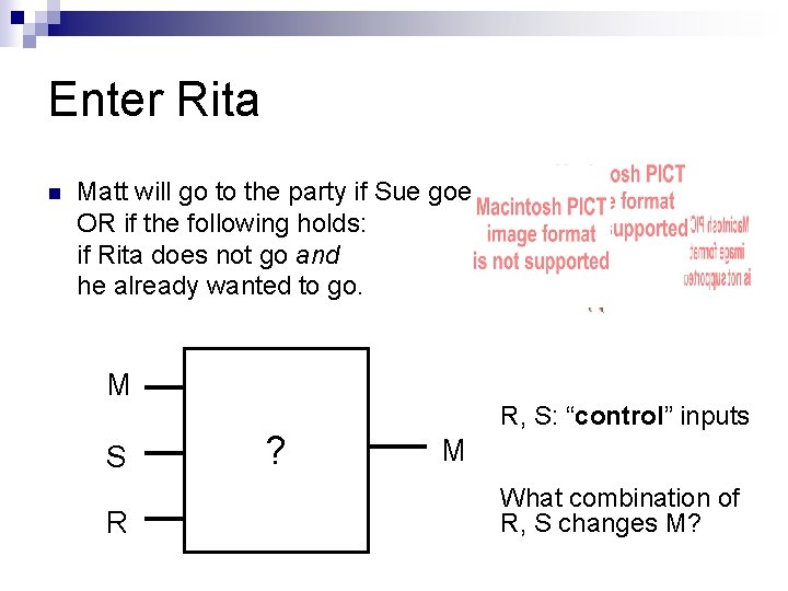
Enter Rita n Matt will go to the party if Sue goes OR if the following holds: if Rita does not go and he already wanted to go. M S R ? R, S: “control” inputs M What combination of R, S changes M?

R-S Flip-Flop S R M

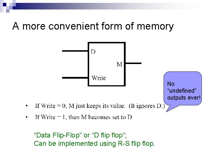
A more convenient form of memory No “undefined” outputs ever! “Data Flip-Flop” or “D flip flop”; Can be implemented using R-S flip flop.

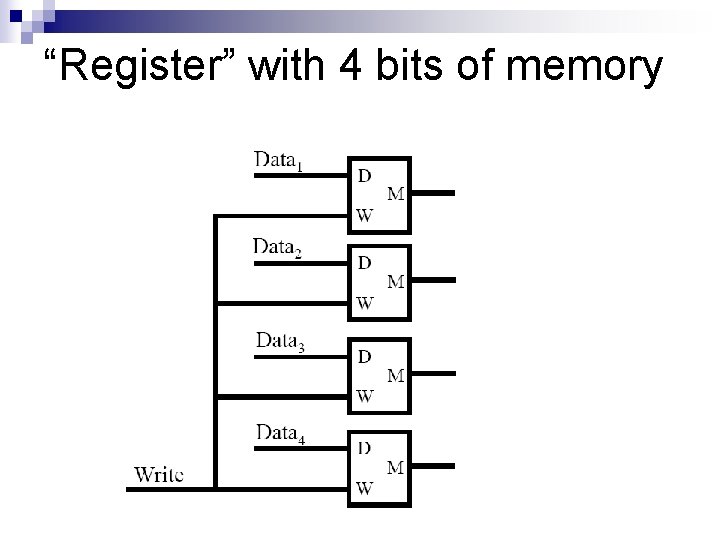
“Register” with 4 bits of memory

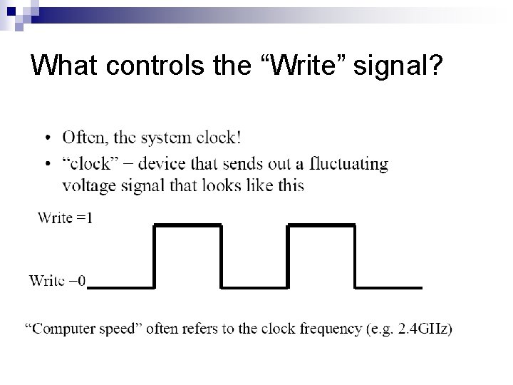
What controls the “Write” signal?

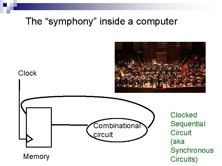
The “symphony” inside a computer Clock Combinational circuit Memory Clocked Sequential Circuit (aka Synchronous Circuits)

Clocked Sequential Circuits

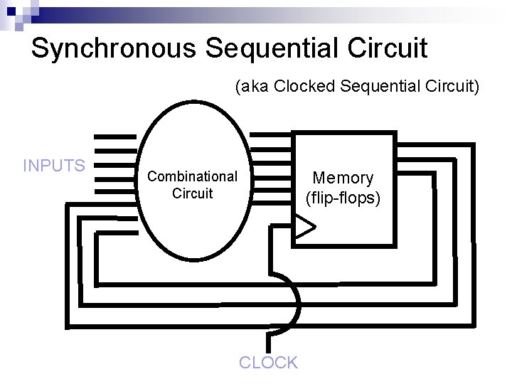
Synchronous Sequential Circuit (aka Clocked Sequential Circuit) INPUTS Memory (flip-flops) Combinational Circuit CLOCK

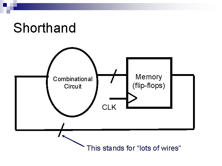
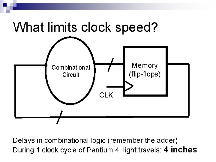
Shorthand Memory (flip-flops) Combinational Circuit CLK This stands for “lots of wires”

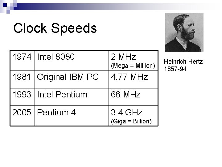
Clock Speeds 1974 Intel 8080 2 MHz (Mega = Million) 1981 Original IBM PC 4. 77 MHz 1993 Intel Pentium 66 MHz 2005 Pentium 4 3. 4 GHz (Giga = Billion) Heinrich Hertz 1857 -94

What limits clock speed? Memory (flip-flops) Combinational Circuit CLK Delays in combinational logic (remember the adder) During 1 clock cycle of Pentium 4, light travels: 4 inches

Finite State Machines Read handout (Brian Hayes article) for next time.

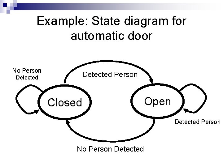
Example: State diagram for automatic door No Person Detected Closed Open Detected Person No Person Detected