Microcomputer system design NAM S B MDLAB Electronic

Microcomputer system design NAM S. B MDLAB. Electronic Engineering, KNU Microcomputer System Design 2015년 2학기 강원대학교 전자공학과 남 시 병 1

Microcomputer system design NAM S. B MDLAB. Electronic Engineering, KNU Microprocessor & embedded 관련 교과목 교육과정 학기 관련교과목 내용 2 -1 Digital 공학 논리회로, 레지스터, 카운 터등 2 -2 Microprocessor 8 bit Microprocessor 기초 3 -1 Microprocessor 실습 및 설계 3 -2 Interface 4 -1 Embedded System 4 -2 Embedded System 응용 VHDL(디지털 시 스템 설계) Atmega 128 interface Computer System Design & Interface Embedded system 2

Microcomputer system design NAM S. B MDLAB. Electronic Engineering, KNU 목차 1. Introduction to microcomputer system 2. Microcomputer system design using Atmega 128 3. Memory interface & Data read write 4. LCD interface 5. LED interface I/O port 6. Key Board interface 7. ADC interface 8. Embedded System 9. Linux & Beaglebone 10. Beaglebone GPIO 11. Beaglebone LCD 12. Beaglebone Sattic IP 13. Beaglebone ADC 14. Beaglebone Web. Cam 15. Beaglebone Project 3

Microcomputer system design 4 NAM S. B MDLAB. Electronic Engineering, KNU 1. Introduction to microcomputer system 차이점 l Microprocessor & Microcontroller system & One chip microprocessor CPU IO PORT Interface Driver I/O device l Microcomputer system Conrrol bus Data bus Address bus Memory CPU I/O address Interface Driver I/O device
")
Microcomputer system design NAM S. B MDLAB. Electronic Engineering, KNU 메모리 인터페이스 설계 1) 설계 순서 (1) Memory 영역 분석 (2) Memory device 결정 (3) Memory Map 구성 (4) Address table 구성 (5) 회로설계 ex 1) EPROM 2716을 4000 H - 47 FFH번지에 설계하여라 (1) Address 영역 4000 -47 FF FFFFH (2) EPROM 2716 address( A 0 - A 10) (3) Memory map 47 FFH 4000 H 0000 H 5 ROM 영역 5
 Address table A")
Microcomputer system design NAM S. B MDLAB. Electronic Engineering, KNU (4) Address table A 15 A 14 A 13 A 12 A 11 A 10 A 9 A 8 A 7 A 6 A 5 A 4 A 3 A 2 A 1 A 0 0 1 0 0 0 0 1 0 0 0 1 1 1 Chip select (5) 회로설계 6 ROM address 고유 영역(A 0 -A 10) 영역 4000 H ROM 47 FFH 6
 아래")
Microcomputer system design 7 NAM S. B MDLAB. Electronic Engineering, KNU ex 4) 아래 Memory map에 의해 ROM과 RAM을 설계하시오 (1) Address 영역 ROM : 0000 H – 07 FFH RAM : 2000 H- 27 FFH (2) ROM 2716 SRAM MC 6116 address( A 0 – A 10) (3) Memory map FFFFH 27 FFH RAM 2000 H 07 FFH ROM 0000 H (4) Address table A 15 A 14 A 13 A 12 A 11 A 10 A 9 A 8 A 7 A 6 A 5 A 4 A 3 A 2 A 1 A 0 0 0 0 0 0 1 1 1 1 1 0000 H ROM 07 FFH 0 0 1 0 0 0 0 1 0 0 1 1 1 2000 H RAM 27 FFH Chip select 7 Memory address 고유 영역(A 0 -A 10) 영역
 회로설계 CPU A")
Microcomputer system design NAM S. B MDLAB. Electronic Engineering, KNU (5) 회로설계 CPU A 0 -A 10 Address bus(A 0 – A 10 ) A 0 – A 10 /RD /WR /MREQ /IORQ /OE /CE A 0 – A 10 /OE /WE /CE ROM (2716) D 0 - D 7 D 0 D 0 - D 7 A 15 A 14 A 13 A 12 A 11 D 0 - D 7 Data bus (D 0 - D 7) 0 0 0 A 15 A 14 A 13 A 12 A 11 0000 H 8 RAM (6116) 0 0 1 0 0 2000 H 8

Microcomputer system design 9 NAM S. B MDLAB. Electronic Engineering, KNU Decoder를 이용한 Memory 영역설계 ü Decoder 74138 3*8 Decoder truth table 74138 3*8 Decoder B C D 0 D 1 D D 2 3 D 4 D 5 D 6 D 7 0 0 1 1 1 1 0 1 1 1 A D 0 0 1 1 1 0 1 1 B D 1 1 0 0 1 1 1 C D 2 1 0 1 1 D 3 1 1 0 1 1 1 1 0 D 4 9 A G 1 D 5 G 2 D 6 G 3 D 7 G 1=1, G 2=0, G 3=0일때 74138이 Active가 된다

Microcomputer system design NAM S. B MDLAB. Electronic Engineering, KNU Decoder를 이용한 Map 설정 Address table A 15 A 14 A 13 A 12 A 11 A 10 A 9 A 8 A 7 A 6 A 5 A 4 A 3 A 2 A 1 A 0 0 0 0 0 0 1 1 1 1 1 0000 H 07 FFH 0 0 1 0 0 0 0 1 1 1 0800 H 0 FFFH 74138 Decoder 입 력 Chip En 영역 Memory address 고유 영역(A 0 -A 10) Map 영역 분할 10 10
 아래 Memory")
Microcomputer system design 11 NAM S. B MDLAB. Electronic Engineering, KNU ex) 아래 Memory map에 의해 ROM을 설계하시오 (1) Address 영역 ROM : 0000 H – 07 FFH ROM : 0800 H – 0 FFFH ROM : 1000 H – 17 FFH (2) ROM 2716 address( A 0 – A 10) (3) Memory map FFFFH 17 FFH 1000 H 0 FFFH ROM_3 ROM_2 0800 H 07 FFH 0000 H Address table A 15 A 14 A 13 A 12 A 11 A 10 A 9 A 8 A 7 A 6 A 5 A 4 A 3 A 2 A 1 A 0 0 0 0 0 0 1 1 1 0 0 0 0 0 1 1 1 0 0 0 1 0 0 0 0 1 1 1 74138 Decoder Chip En 11 ROM_1 Memory address 고유 영역(A 0 -A 10) 영역 0000 H 07 FFH 0800 H 0 FFFH 1000 H 17 FFH
 회로설계 12 NAM S. B MDLAB. Electronic Engineering, KNU 12")
Microcomputer system design (5) 회로설계 12 NAM S. B MDLAB. Electronic Engineering, KNU 12
 microprocessor ü")
Microcomputer system design NAM S. B MDLAB. Electronic Engineering, KNU Intel 계열(8085) microprocessor ü 8085 microprocessor 외부 핀 X 1 X 2 RESET OUT SOD SID TRAP RST 7. 5 RST 6. 5 RST 5. 5 INTR /INTA HOLD HLDA RESET IN READY IO/M S 1 /RD /WR ALE 13 AD 0 -AD 7 Address data bus AD 0 -AD 7 INTEL 8085 8 bit microprocessor A 8 -A 15 address bus A 8 -A 15 그림 2 -12. 8085 CPU 13

Microcomputer system design NAM S. B MDLAB. Electronic Engineering, KNU 14 Demultiplexed address interface Intel 계열 CPU는 하위 주소버스는 데이터 버스와 동일한 버스를 사용하도록 설계되어 있다. 따라서 외부 에서 주소와 데이터버스를 분리 시켜주는 회로가 필요하다. 이 방법을 demultiplexed address interface 가고 한다. LATCH AD 0 -AD 7 ALE A 0 -A 7 Address bus Data bus A 0 -A 15 D 0 -D 7 A 8 -A 15 CPU에서 먼저 address 신호를 출력한 다음 ALE( Address Latch Enable)에 의하여 address를 래치 한다. 이때 address bus 는 A 0 -A 7을 구성하고 A 8 -A 15을 합성하면 A 0 -A 15까 된다. 데이터 신호는 address 신호다음에 ALE가 “Low” 일 때에 출력된다. 14

Microcomputer system design NAM S. B MDLAB. Electronic Engineering, KNU Demultiplexed address interface AD 0 -AD 7 address data ALE A 0 -A 7 Address A 0 -A 7 A 8 -A 15 Address A 8 -A 15 D 0 -D 7 data { A 0 -A 15 ① AD 0 -AD 7(하위 8비트 버스)에 주소 신호(A 0 -A 7)를 출력한다 ② ALE신호가 “high”로 되면서 래치회로에서 A 0 -A 7을 래치한다. ③ ALE신호를 “low”로 전환하고 D 0 -D 7 를 출력한다. 15 15

Microcomputer system design NAM S. B MDLAB. Electronic Engineering, KNU 8085 Demultiplexed address bus 방식 회로 16 16

Microcomputer system design NAM S. B MDLAB. Electronic Engineering, KNU ATmega 128 CPU Pinout AD 0 -AD 7 PORTA ALE: PORTG. 2 A 8 -A 15 PORTC /RD: PORTG. 1 /WR: PORTG. 0 17

Microcomputer system design NAM S. B MDLAB. Electronic Engineering, KNU Address Latch Requirements : Demultiplexed addressing method 18

Microcomputer system design NAM S. B MDLAB. Electronic Engineering, KNU 19

Microcomputer system design NAM S. B MDLAB. Electronic Engineering, KNU Input Output Device interface ü Input Output Device 종류 Micro-computer system CPU Bus Interface 회로 Bus I/O device Buffer, 기타 Interface 회로 • Input Device : Key Board, Mouse, Tablet, AD converter 등 • Output Device : CRT display, 7 segment, LCD, Printer, Plotter, DA converter 등 • I/O device : Memory, Magnetic tape, HDD, FDD 20 20

Microcomputer system design NAM S. B MDLAB. Electronic Engineering, KNU 주소에 의한 I/O device(Input Output Device) interface 방식 (1)Memory Mapped I/O방식 (2) I/O Mapped I/O(Isolated Mapped I/O방식 Main memory FFFF I/O memory FF I/O address 0000 l Main memory 내부에 I/O address 영역을 두는 방식 l 회로가 간단하다 l Main memory 영역 감소 21 0000 I/O address 00 l Main memory 영역과 I/O address 영역을 분리 시켜서 설계된 방식 l회로가 복잡하다 lmain memory 영역을 모두 사용 가 능 21

Microcomputer system design NAM S. B MDLAB. Electronic Engineering, KNU ATmega 128 CPU module configuration 22

Microcomputer system design ATmega 128 CPU Pin out NAM S. B MDLAB. Electronic Engineering, KNU 23

Microcomputer system design NAM S. B MDLAB. Electronic Engineering, KNU ATmega 128 Microcomputer system 24

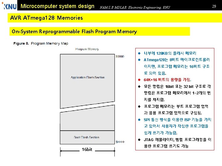
Microcomputer system design NAM S. B MDLAB. Electronic Engineering, KNU Features • High-performance, Low-power AVR® 8 -bit Microcontroller • Advanced RISC Architecture – 133 Powerful Instructions – Most Single Clock Cycle Execution – 32 x 8 General Purpose Working Registers + Peripheral Control Registers – Fully Static Operation – Up to 16 MIPS Throughput at 16 MHz – On-chip 2 -cycle Multiplier • Nonvolatile Program and Data Memories – 128 K Bytes of In-System Reprogrammable Flash Endurance: 10, 000 Write/Erase Cycles – Optional Boot Code Section with Independent Lock Bits In-System Programming by On-chip Boot Program True Read-While-Write Operation – 4 K Bytes EEPROM Endurance: 100, 000 Write/Erase Cycles – 4 K Bytes Internal SRAM – Up to 64 K Bytes Optional External Memory Space – Programming Lock for Software Security – SPI Interface for In-System Programming • JTAG (IEEE std. 1149. 1 Compliant) Interface – Boundary-scan Capabilities According to the JTAG Standard – Extensive On-chip Debug Support – Programming of Flash, EEPROM, Fuses and Lock Bits through the JTAG Interface 25

Microcomputer system design NAM S. B MDLAB. Electronic Engineering, KNU • Peripheral Features – Two 8 -bit Timer/Counters with Separate Prescalers and Compare Modes – Two Expanded 16 -bit Timer/Counters with Separate Prescaler, Compare Mode and Capture Mode – Real Time Counter with Separate Oscillator – Two 8 -bit PWM Channels – 6 PWM Channels with Programmable Resolution from 2 to 16 Bits – Output Compare Modulator – 8 -channel, 10 -bit ADC 8 Single-ended Channels 7 Differential Channels 2 Differential Channels with Programmable Gain at 1 x, 10 x, or 200 x – Byte-oriented Two-wire Serial Interface – Dual Programmable Serial USARTs – Master/Slave SPI Serial Interface – Programmable Watchdog Timer with On-chip Oscillator – On-chip Analog Comparator • Special Microcontroller Features – Power-on Reset and Programmable Brown-out Detection – Internal Calibrated RC Oscillator – External and Internal Interrupt Sources – Six Sleep Modes: Idle, ADC Noise Reduction, Power-save, Power-down, Standby, and Extended Standby – Software Selectable Clock Frequency – ATmega 103 Compatibility Mode Selected by a Fuse – Global Pull-up Disable 26

Microcomputer system design NAM S. B MDLAB. Electronic Engineering, KNU • I/O and Packages – 53 Programmable I/O Lines – 64 -lead TQFP and 64 -pad MLF • Operating Voltages – 2. 7 - 5. 5 V for ATmega 128 L – 4. 5 - 5. 5 V for ATmega 128 • Speed Grades – 0 - 8 MHz for ATmega 128 L – 0 - 16 MHz for ATmega 128 27

Microcomputer system design 28 NAM S. B MDLAB. Electronic Engineering, KNU ATmega 128 microcomputer design Memory & IO design l Bus system ü address bus : 16 bit ü data bus : 8 bit ü control bus System bus Bus Conltrol Bus Data Address Bus Address bus Data bus ATmega 128 Control bus Data bus External Memory Control bus Address bus Data bus Control bus I/O

Microcomputer system design 사용가능 영역 NAM S. B MDLAB. Electronic Engineering, KNU 31
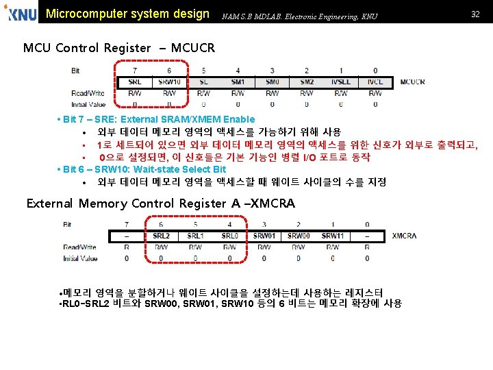

Microcomputer system design NAM S. B MDLAB. Electronic Engineering, KNU 33 ØSRL 2∼SRL 0 (Wait State Sector Limit) 비트 • 메모리를 2개의 섹터로 구분하는 기능을 담당 ØSRW 11와 SRW 10 비트 (Wait-state Select Bits for Upper Sector) • MCUCR의 SRW 10 비트와 XMCUCR의 SRW 11 비트를 조합하여 외부 데이터 메모리의 상위 섹 터에 해당하는 영역의 웨이트 사이클을 설정 ØSRW 01과 SRW 00 비트 (Wait-state Select Bits for Lower Sector) • 외부 데이터 메모리의 하위 섹터에 해당하는 영역의 웨이트 사이클을 설정

Microcomputer system design NAM S. B MDLAB. Electronic Engineering, KNU 34

Microcomputer system design NAM S. B MDLAB. Electronic Engineering, KNU Atmega 128: External SRAM 64 K Interface l. External SRAM : 64 Kbyte l. Wait cycle : 2 cycle 35

Microcomputer system design MCUCR 36 NAM S. B MDLAB. Electronic Engineering, KNU SRE SRW 10 SE SM 1 SM 0 SM 2 IVSEL 1 0 0 0 IVCE SRE: External SRAM/XMEM Enable XMCRA - SRL 2 SRL 1 SRL 0 SRW 01 SRW 00 SRW 11 0 0 0 1 Upper memory block ; 0 x 1100~0 x. FFFF Wait: 2 cycle -

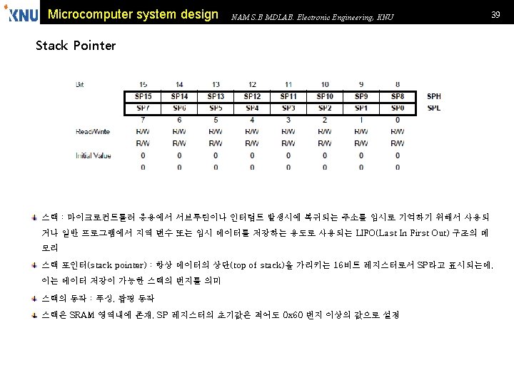
Microcomputer system design NAM S. B MDLAB. Electronic Engineering, KNU Status Register l Bit 7 (I) : Global Interrupt Enable l Bit 6 (T) : 비트 복사 저장 (Bit Copy Storage) l Bit 5 (H) : 보조 캐리 플래그 (Half Carry Flag) l Bit 4 (S) : Sign Bit l Bit 3 (V) : 2의 보수 오버플로우 비트 (two's complement overflow bit) l Bit 2 (N) : Negative Flag l Bit 1 (Z) : Zero Flag l Bit 0 (C) : Carry Flag 37

Microcomputer system design address 영역 Access time 0 x. FFFF 0 x 8000 SDRAM 빠름 0 x 7 FFF 0 x 1100 I/O 영역 느림 0 x 10 FF 0 x 0000 System 영역 NAM S. B MDLAB. Electronic Engineering, KNU 43
- Slides: 43