Lecture 11 Sequential Circuit Design 11 Sequential Circuits
- Slides: 35

Lecture 11: Sequential Circuit Design 11: Sequential Circuits 1

Outline q q q Sequencing Element Design Max and Min-Delay Clock Skew Time Borrowing Two-Phase Clocking 11: Sequential Circuits CMOS VLSI Design 4 th Ed. 2

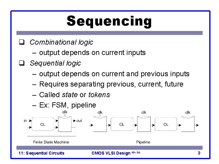
Sequencing q Combinational logic – output depends on current inputs q Sequential logic – output depends on current and previous inputs – Requires separating previous, current, future – Called state or tokens – Ex: FSM, pipeline 11: Sequential Circuits CMOS VLSI Design 4 th Ed. 3

Sequencing Cont. q If tokens moved through pipeline at constant speed, no sequencing elements would be necessary q Ex: fiber-optic cable – Light pulses (tokens) are sent down cable – Next pulse sent before first reaches end of cable – No need for hardware to separate pulses – But dispersion sets min time between pulses q This is called wave pipelining in circuits q In most circuits, dispersion is high – Delay fast tokens so they don’t catch slow ones. 11: Sequential Circuits CMOS VLSI Design 4 th Ed. 4

Sequencing Overhead q Use flip-flops to delay fast tokens so they move through exactly one stage each cycle. q Inevitably adds some delay to the slow tokens q Makes circuit slower than just the logic delay – Called sequencing overhead q Some people call this clocking overhead – But it applies to asynchronous circuits too – Inevitable side effect of maintaining sequence 11: Sequential Circuits CMOS VLSI Design 4 th Ed. 5

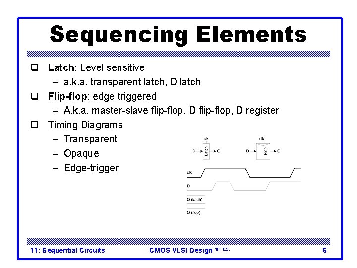
Sequencing Elements q Latch: Level sensitive – a. k. a. transparent latch, D latch q Flip-flop: edge triggered – A. k. a. master-slave flip-flop, D register q Timing Diagrams – Transparent – Opaque – Edge-trigger 11: Sequential Circuits CMOS VLSI Design 4 th Ed. 6

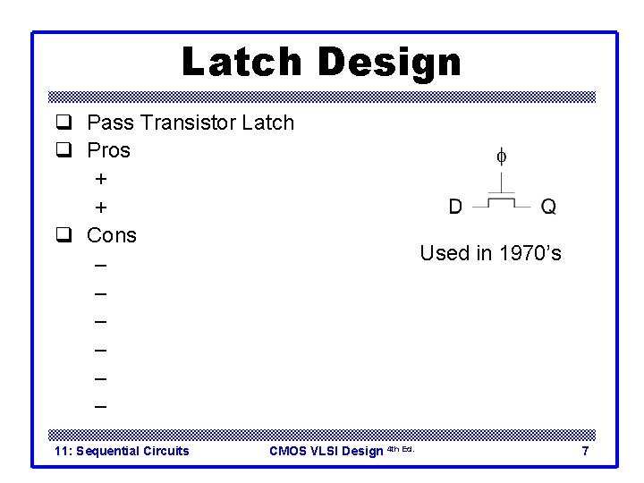
Latch Design q Pass Transistor Latch q Pros + Tiny + Low clock load q Cons – Vt drop – nonrestoring – backdriving – output noise sensitivity – dynamic – diffusion input 11: Sequential Circuits CMOS VLSI Design 4 th Ed. Used in 1970’s 7

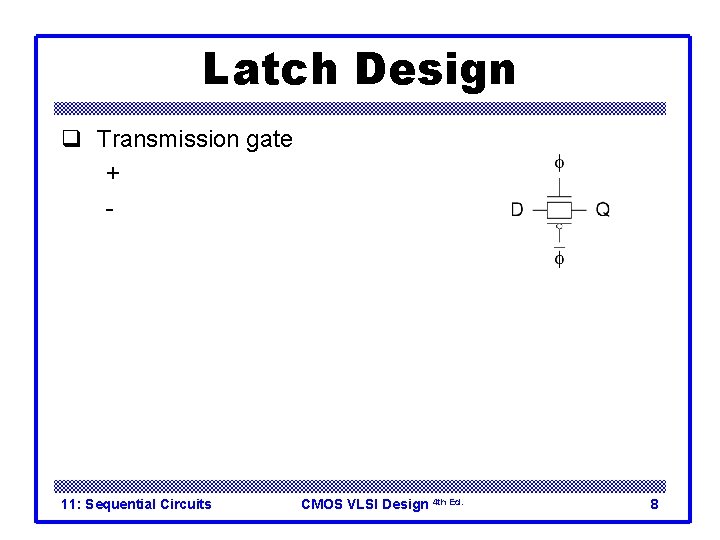
Latch Design q Transmission gate + No Vt drop - Requires inverted clock 11: Sequential Circuits CMOS VLSI Design 4 th Ed. 8

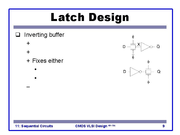
Latch Design q Inverting buffer + Restoring + No backdriving + Fixes either • Output noise sensitivity • Or diffusion input – Inverted output 11: Sequential Circuits CMOS VLSI Design 4 th Ed. 9

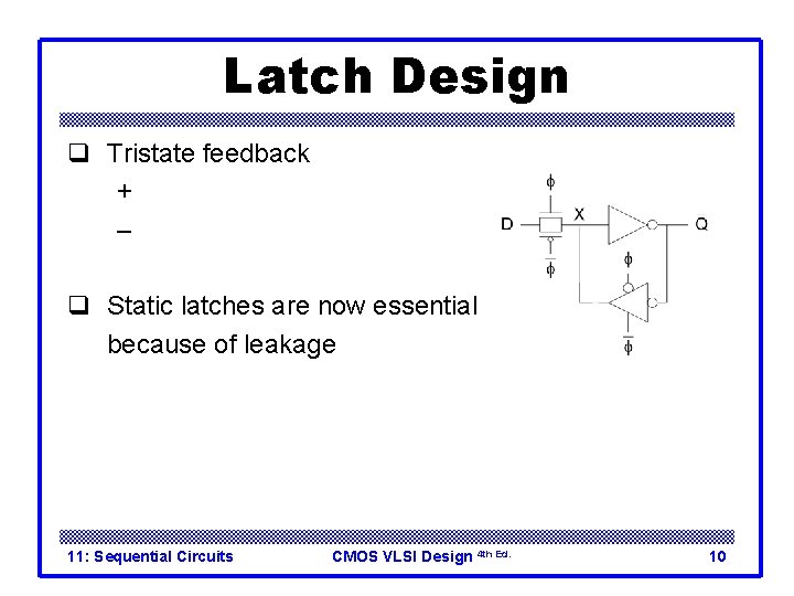
Latch Design q Tristate feedback + Static – Backdriving risk q Static latches are now essential because of leakage 11: Sequential Circuits CMOS VLSI Design 4 th Ed. 10

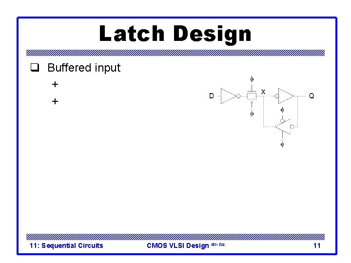
Latch Design q Buffered input + Fixes diffusion input + Noninverting 11: Sequential Circuits CMOS VLSI Design 4 th Ed. 11

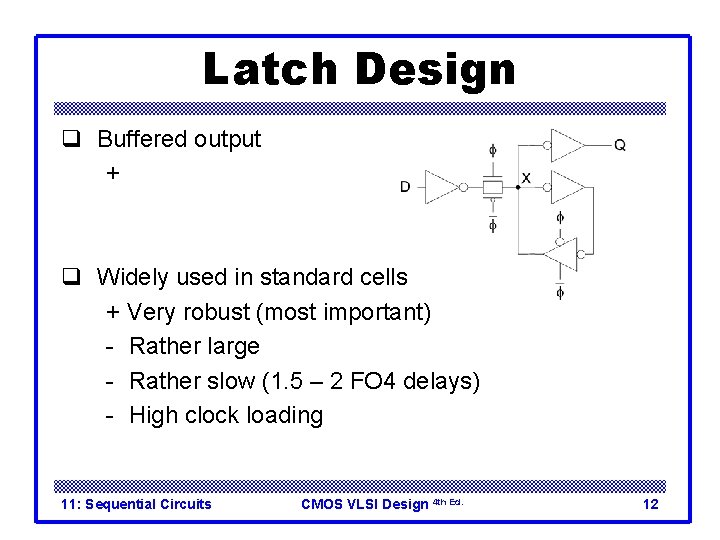
Latch Design q Buffered output + No backdriving q Widely used in standard cells + Very robust (most important) - Rather large - Rather slow (1. 5 – 2 FO 4 delays) - High clock loading 11: Sequential Circuits CMOS VLSI Design 4 th Ed. 12

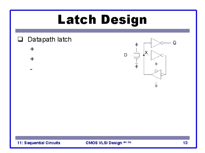
Latch Design q Datapath latch + smaller + faster - unbuffered input 11: Sequential Circuits CMOS VLSI Design 4 th Ed. 13

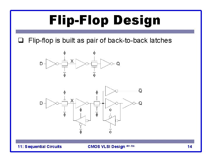
Flip-Flop Design q Flip-flop is built as pair of back-to-back latches 11: Sequential Circuits CMOS VLSI Design 4 th Ed. 14

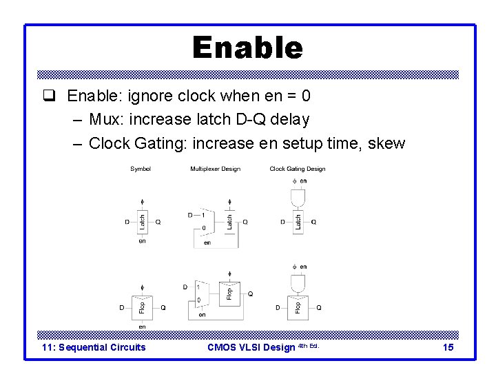
Enable q Enable: ignore clock when en = 0 – Mux: increase latch D-Q delay – Clock Gating: increase en setup time, skew 11: Sequential Circuits CMOS VLSI Design 4 th Ed. 15

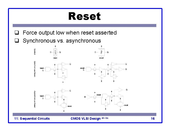
Reset q Force output low when reset asserted q Synchronous vs. asynchronous 11: Sequential Circuits CMOS VLSI Design 4 th Ed. 16

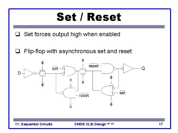
Set / Reset q Set forces output high when enabled q Flip-flop with asynchronous set and reset 11: Sequential Circuits CMOS VLSI Design 4 th Ed. 17

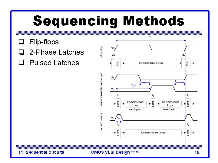
Sequencing Methods q Flip-flops q 2 -Phase Latches q Pulsed Latches 11: Sequential Circuits CMOS VLSI Design 4 th Ed. 18

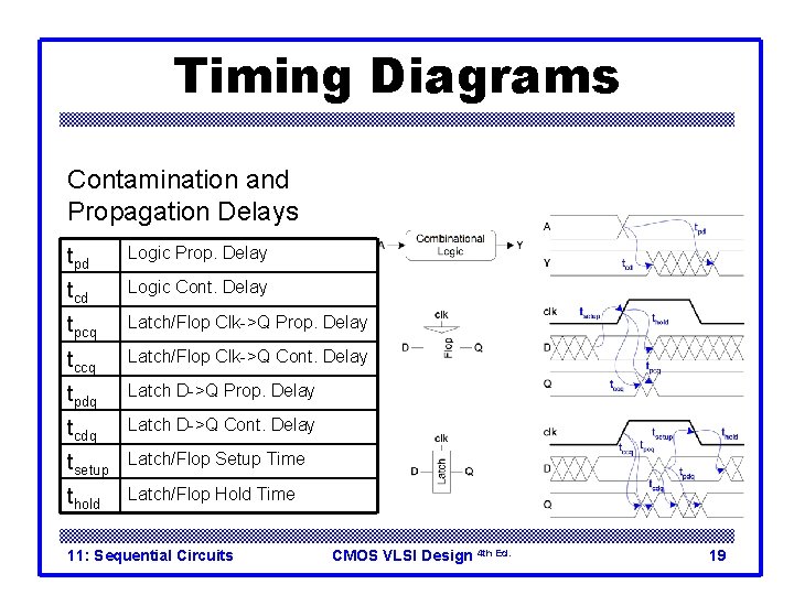
Timing Diagrams Contamination and Propagation Delays tpd Logic Prop. Delay tcd Logic Cont. Delay tpcq Latch/Flop Clk->Q Prop. Delay tccq Latch/Flop Clk->Q Cont. Delay tpdq Latch D->Q Prop. Delay tcdq Latch D->Q Cont. Delay tsetup Latch/Flop Setup Time thold Latch/Flop Hold Time 11: Sequential Circuits CMOS VLSI Design 4 th Ed. 19

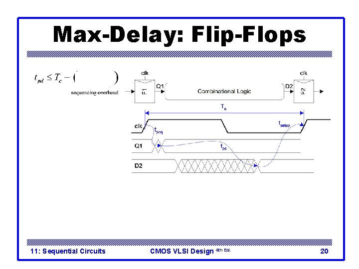
Max-Delay: Flip-Flops 11: Sequential Circuits CMOS VLSI Design 4 th Ed. 20

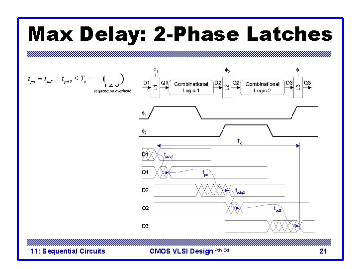
Max Delay: 2 -Phase Latches 11: Sequential Circuits CMOS VLSI Design 4 th Ed. 21

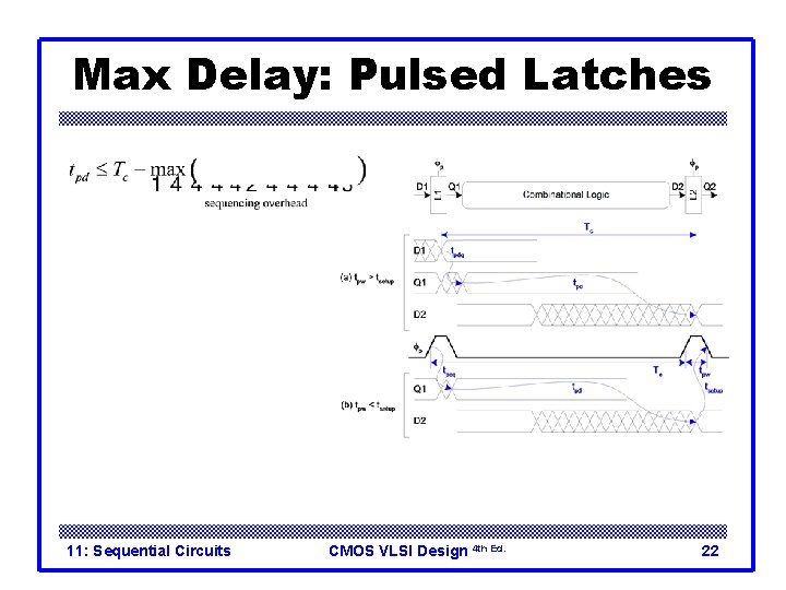
Max Delay: Pulsed Latches 11: Sequential Circuits CMOS VLSI Design 4 th Ed. 22

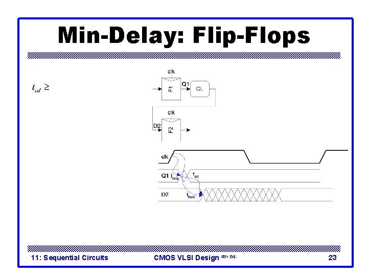
Min-Delay: Flip-Flops 11: Sequential Circuits CMOS VLSI Design 4 th Ed. 23

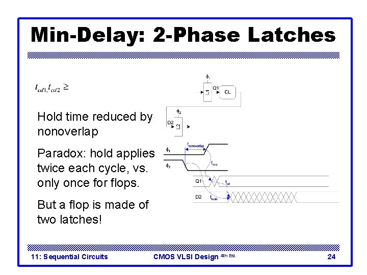
Min-Delay: 2 -Phase Latches Hold time reduced by nonoverlap Paradox: hold applies twice each cycle, vs. only once for flops. But a flop is made of two latches! 11: Sequential Circuits CMOS VLSI Design 4 th Ed. 24

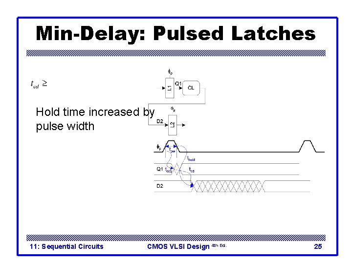
Min-Delay: Pulsed Latches Hold time increased by pulse width 11: Sequential Circuits CMOS VLSI Design 4 th Ed. 25

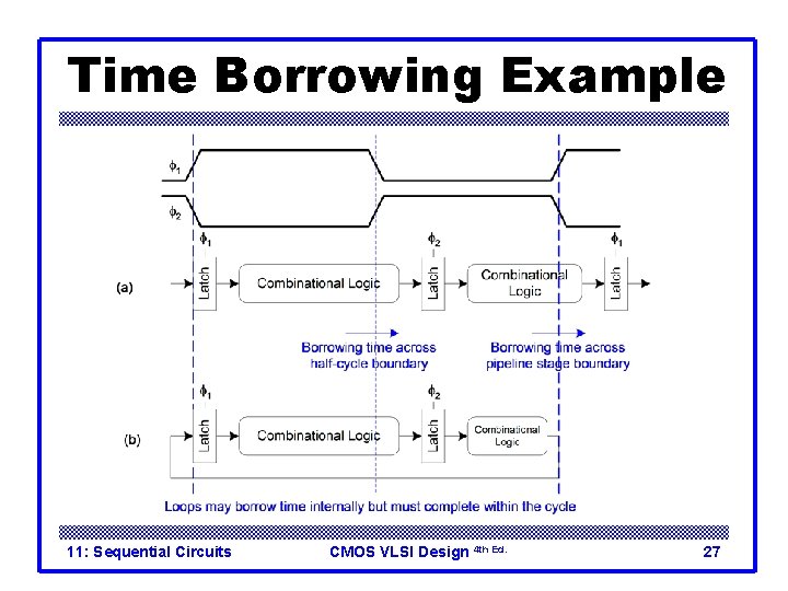
Time Borrowing q In a flop-based system: – Data launches on one rising edge – Must setup before next rising edge – If it arrives late, system fails – If it arrives early, time is wasted – Flops have hard edges q In a latch-based system – Data can pass through latch while transparent – Long cycle of logic can borrow time into next – As long as each loop completes in one cycle 11: Sequential Circuits CMOS VLSI Design 4 th Ed. 26

Time Borrowing Example 11: Sequential Circuits CMOS VLSI Design 4 th Ed. 27

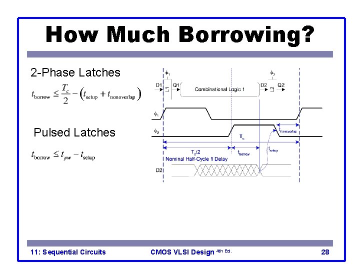
How Much Borrowing? 2 -Phase Latches Pulsed Latches 11: Sequential Circuits CMOS VLSI Design 4 th Ed. 28

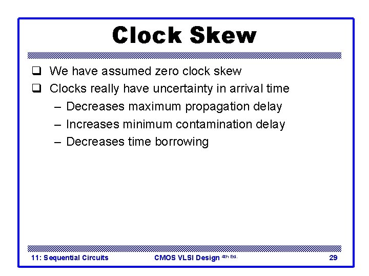
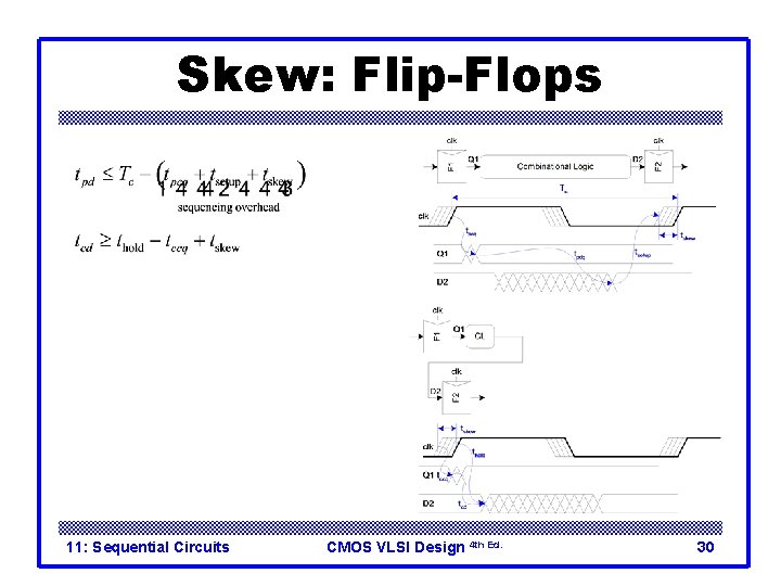
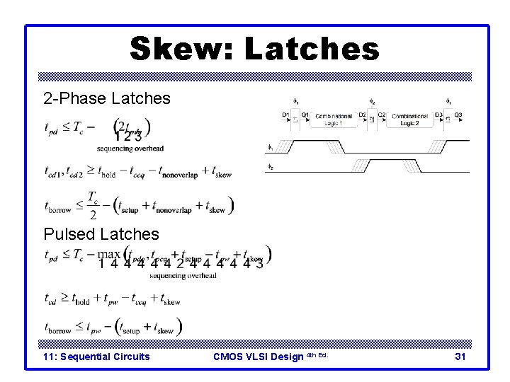
Clock Skew q We have assumed zero clock skew q Clocks really have uncertainty in arrival time – Decreases maximum propagation delay – Increases minimum contamination delay – Decreases time borrowing 11: Sequential Circuits CMOS VLSI Design 4 th Ed. 29

Skew: Flip-Flops 11: Sequential Circuits CMOS VLSI Design 4 th Ed. 30

Skew: Latches 2 -Phase Latches Pulsed Latches 11: Sequential Circuits CMOS VLSI Design 4 th Ed. 31

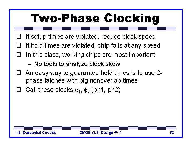
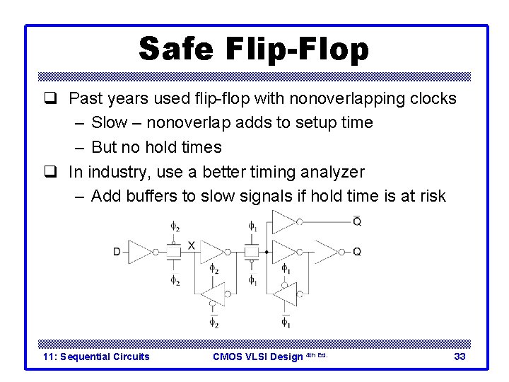
Two-Phase Clocking q If setup times are violated, reduce clock speed q If hold times are violated, chip fails at any speed q In this class, working chips are most important – No tools to analyze clock skew q An easy way to guarantee hold times is to use 2 phase latches with big nonoverlap times q Call these clocks f 1, f 2 (ph 1, ph 2) 11: Sequential Circuits CMOS VLSI Design 4 th Ed. 32

Safe Flip-Flop q Past years used flip-flop with nonoverlapping clocks – Slow – nonoverlap adds to setup time – But no hold times q In industry, use a better timing analyzer – Add buffers to slow signals if hold time is at risk 11: Sequential Circuits CMOS VLSI Design 4 th Ed. 33

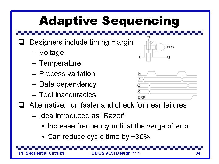
Adaptive Sequencing q Designers include timing margin – Voltage – Temperature – Process variation – Data dependency – Tool inaccuracies q Alternative: run faster and check for near failures – Idea introduced as “Razor” • Increase frequency until at the verge of error • Can reduce cycle time by ~30% 11: Sequential Circuits CMOS VLSI Design 4 th Ed. 34

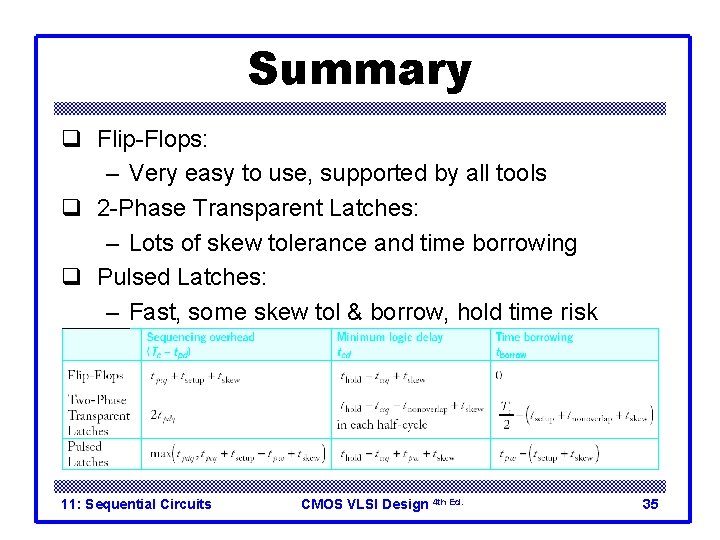
Summary q Flip-Flops: – Very easy to use, supported by all tools q 2 -Phase Transparent Latches: – Lots of skew tolerance and time borrowing q Pulsed Latches: – Fast, some skew tol & borrow, hold time risk 11: Sequential Circuits CMOS VLSI Design 4 th Ed. 35