EEE 4084 F Digital Systems Lecture 10 Architectures





- Slides: 55

EEE 4084 F Digital Systems Lecture 10: Architectures Types, Memory Access Architectures, Flynn’s Taxonomy, Classic Microcontroller Case Studies Attribution-Share. Alike 4. 0 International (CC BY-SA 4. 0)

Lecture Overview Classic parallel programming techniques Processor Architecture Types Von Neumann Class activity Flynn’s Taxonomy Memory access architectures Case Studies of classic microprocessor/ microcontroller architectures Additional readings

Classic Parallel EEE 4084 F

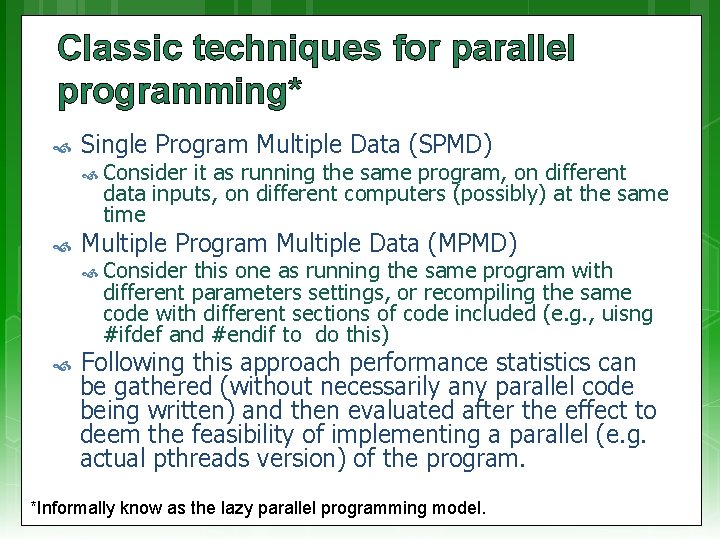
Classic techniques for parallel programming* Single Program Multiple Data (SPMD) Consider it as running the same program, on different data inputs, on different computers (possibly) at the same time Multiple Program Multiple Data (MPMD) Consider this one as running the same program with different parameters settings, or recompiling the same code with different sections of code included (e. g. , uisng #ifdef and #endif to do this) Following this approach performance statistics can be gathered (without necessarily any parallel code being written) and then evaluated after the effect to deem the feasibility of implementing a parallel (e. g. actual pthreads version) of the program. *Informally know as the lazy parallel programming model.

Terms EEE 4084 F

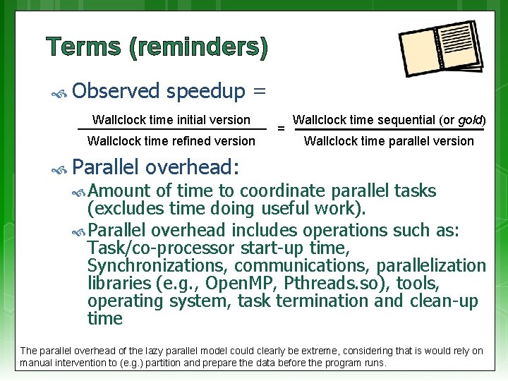
Terms (reminders) Observed speedup = Wallclock time initial version Wallclock time refined version Parallel = Wallclock time sequential (or gold) Wallclock time parallel version overhead: Amount of time to coordinate parallel tasks (excludes time doing useful work). Parallel overhead includes operations such as: Task/co-processor start-up time, Synchronizations, communications, parallelization libraries (e. g. , Open. MP, Pthreads. so), tools, operating system, task termination and clean-up time The parallel overhead of the lazy parallel model could clearly be extreme, considering that is would rely on manual intervention to (e. g. ) partition and prepare the data before the program runs.

Some terms Embarrassingly Parallel Simultaneously performing many similar, independent tasks, with little to no coordination between tasks. Massively Parallel Hardware that has very many processors (execution of parallel tasks). Can consider this classification of 100 000+ parallel tasks. { Stupidly Parallel } While this isn’t really an official term it typically relates to instances where a big (and possibly very complex) coding effort is put into developing a solution that in practice has negligible savings or worse is a whole lot slower (and possibly erroneous/buggy) than if it was just a simpler sequential implementation.

Type A Type F EEE 4084 F Type C D B Type E Type H Type J Type G Type I Types of Processor Architecture

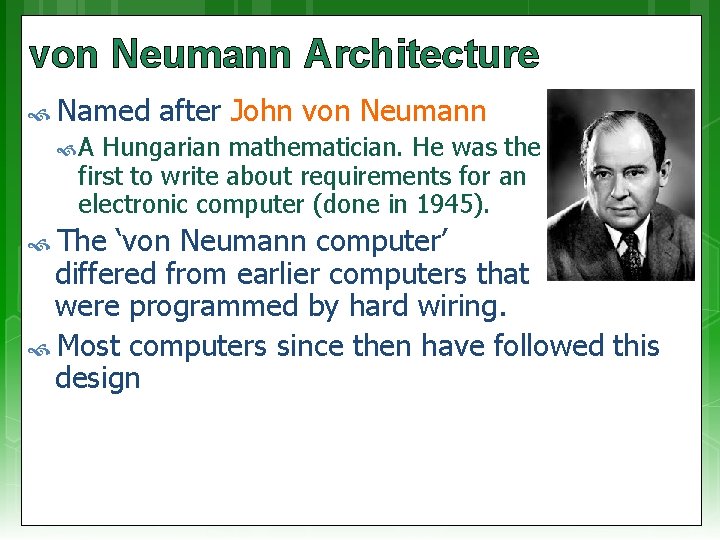
von Neumann Architecture Named after John von Neumann A Hungarian mathematician. He was the first to write about requirements for an electronic computer (done in 1945). The ‘von Neumann computer’ differed from earlier computers that were programmed by hard wiring. Most computers since then have followed this design

John von Neumann & the Jv. N Machine “The Greatest Computer Programmer Was Its First!” https: //www. youtube. com/watch? v=Po 3 vw. Mq_2 x. A

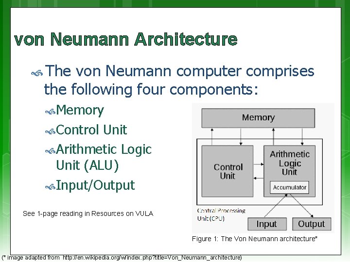
von Neumann Architecture The von Neumann computer comprises the following four components: Memory Control Unit Arithmetic Logic Unit (ALU) Input/Output See 1 -page reading in Resources on VULA Figure 1: The Von Neumann architecture* (* image adapted from http: //en. wikipedia. org/w/index. php? title=Von_Neumann_architecture)

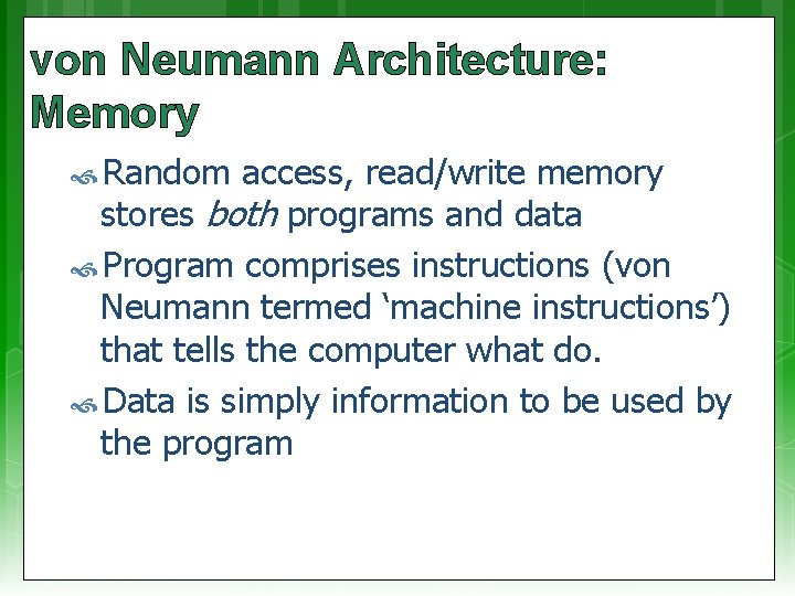
von Neumann Architecture: Memory Random access, read/write memory stores both programs and data Program comprises instructions (von Neumann termed ‘machine instructions’) that tells the computer what do. Data is simply information to be used by the program

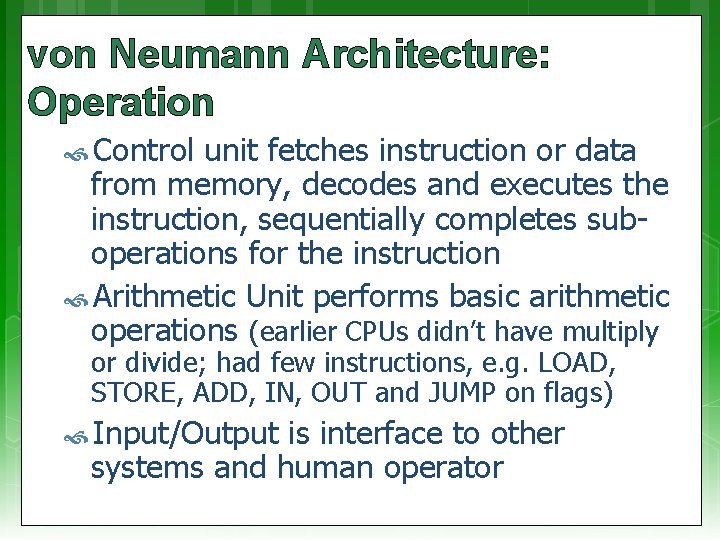
von Neumann Architecture: Operation Control unit fetches instruction or data from memory, decodes and executes the instruction, sequentially completes suboperations for the instruction Arithmetic Unit performs basic arithmetic operations (earlier CPUs didn’t have multiply or divide; had few instructions, e. g. LOAD, STORE, ADD, IN, OUT and JUMP on flags) Input/Output is interface to other systems and human operator

Suggested further learning Simple recap of Von Neumann Arch: http: //www. youtube. com/watch? v=DMi. Eg KZ-q. Cw Some history of Von Neumann leading towards his machine: (not examined!) “The Greatest Computer Programmer Was Its First” http: //www. youtube. com/watch? v=Po 3 vw Mq_2 x. A

n o V n n a m u e N Ha rv a rd The Big Competitor… The Harvard Architecture EEE 4084 F

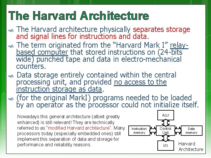
The Harvard Architecture The Harvard architecture physically separates storage and signal lines for instructions and data. The term originated from the “Harvard Mark I” relaybased computer that stored instructions on (24 -bits wide) punched tape and data in electro-mechanical counters. Data storage entirely contained within the central processing unit, and provided no access to the instruction storage as data. (for the original Mark. I) programs needed to be loaded by an operator as the processor could not initialize itself. Nowadays this general architecture (albeit greatly enhanced) is still relevant! They are technically referred to as “modified Harvard architecture”. Many processors today (especially embedded ones) still implement this separation of data and storage for performance and reliability reasons. ALU Instruction memory Control Unit Data memory I/O Harvard Architecture

The Harvard Mark I “Harvard Mark I” https: //www. youtube. com/watch? v=4 Obouw. CHk 8 w

Type A Type F Type C D B Type E Type H Type J Type G Type I EEE 4084 F Flynns Taxonomy of Processor Architectures

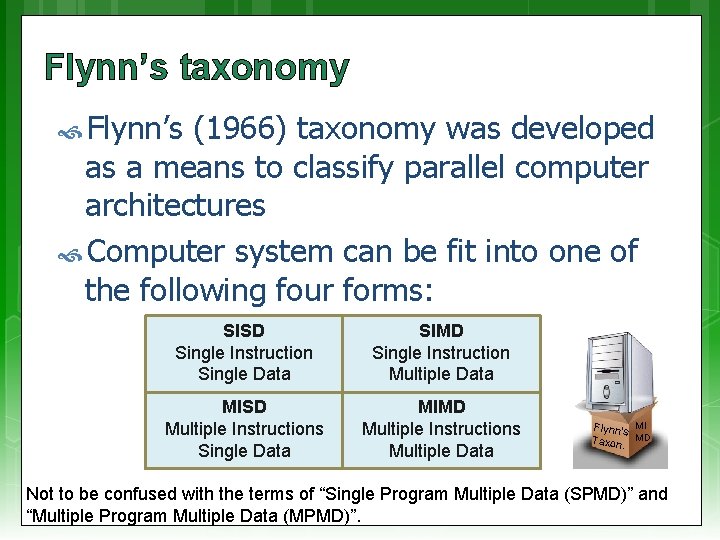
Flynn’s taxonomy Flynn’s (1966) taxonomy was developed as a means to classify parallel computer architectures Computer system can be fit into one of the following four forms: SISD Single Instruction Single Data SIMD Single Instruction Multiple Data MISD Multiple Instructions Single Data MIMD Multiple Instructions Multiple Data Flynn’s MI Taxon. MD Not to be confused with the terms of “Single Program Multiple Data (SPMD)” and “Multiple Program Multiple Data (MPMD)”.

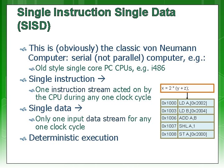
Single Instruction Single Data (SISD) This is (obviously) the classic von Neumann Computer: serial (not parallel) computer, e. g. : Old style single core PC CPUs, e. g. i 486 Single instruction stream acted on by the CPU during any one clock cycle One x = 2 * (y + z); Single data 0 x 1000 LD A, [0 x 2002] Only 0 x 1006 ADD A, B one input data stream for any one clock cycle Deterministic execution 0 x 1003 LD B, [0 x 2004] 0 x 1007 SHL A, 1 0 x 1008 ST A, [0 x 2000]

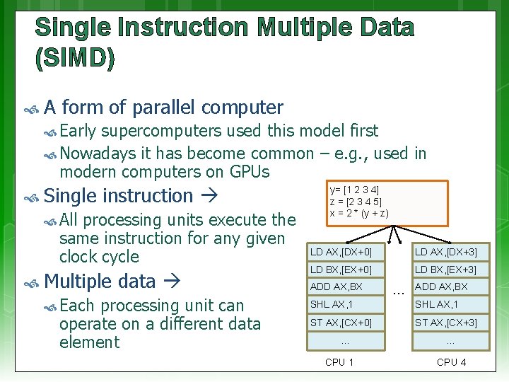
Single Instruction Multiple Data (SIMD) A form of parallel computer Early supercomputers used this model first Nowadays it has become common – e. g. , used in modern computers on GPUs Single instruction All processing units execute the same instruction for any given clock cycle y= [1 2 3 4] z = [2 3 4 5] x = 2 * (y + z) LD AX, [DX+0] LD AX, [DX+3] Multiple data LD BX, [EX+0] LD BX, [EX+3] Each SHL AX, 1 ST AX, [CX+0] ST AX, [CX+3] processing unit can operate on a different data element ADD AX, BX … CPU 1 … ADD AX, BX … CPU 4

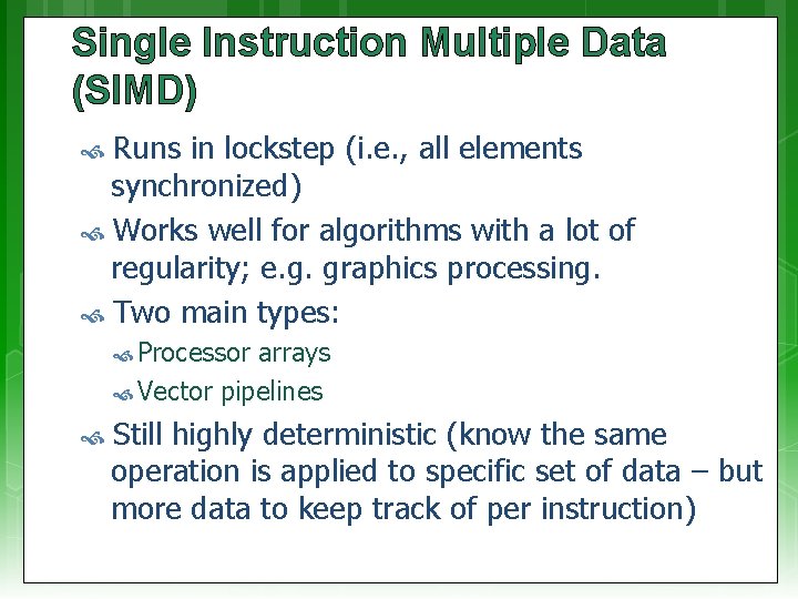
Single Instruction Multiple Data (SIMD) Runs in lockstep (i. e. , all elements synchronized) Works well for algorithms with a lot of regularity; e. g. graphics processing. Two main types: Processor arrays Vector pipelines Still highly deterministic (know the same operation is applied to specific set of data – but more data to keep track of per instruction)

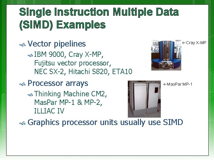
Single Instruction Multiple Data (SIMD) Examples Vector pipelines Cray X-MP IBM 9000, Cray X-MP, Fujitsu vector processor, NEC SX-2, Hitachi S 820, ETA 10 Processor arrays Mas. Par MP-1 Thinking Machine CM 2, Mas. Par MP-1 & MP-2, ILLIAC IV Graphics processor units usually use SIMD

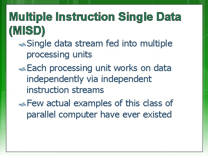
Multiple Instruction Single Data (MISD) Single data stream fed into multiple processing units Each processing unit works on data independently via independent instruction streams Few actual examples of this class of parallel computer have ever existed

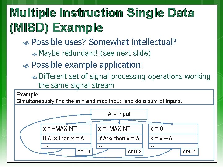
Multiple Instruction Single Data (MISD) Example Possible uses? Somewhat intellectual? Maybe redundant! (see next slide) Possible example application: Different set of signal processing operations working the same signal stream Example: Simultaneously find the min and max input, and do a sum of inputs. A = input x = +MAXINT x = -MAXINT x=0 If A<x then x = A … If A>x then x = A … x=x+A … CPU 1 CPU 2 CPU 3

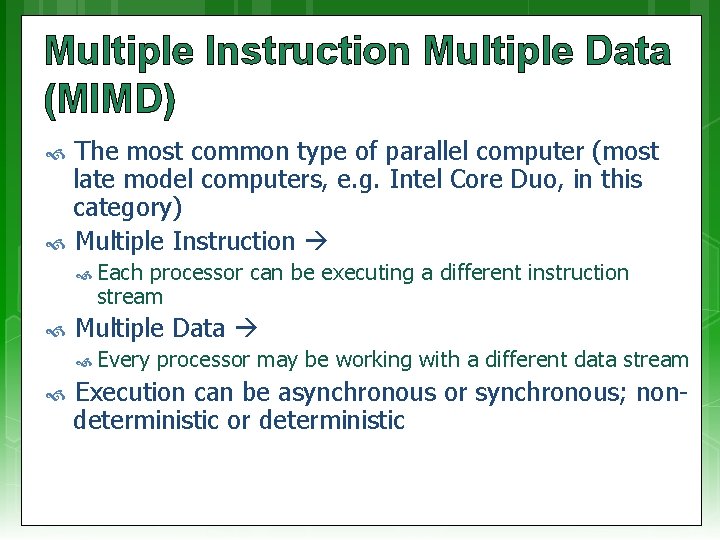
Multiple Instruction Multiple Data (MIMD) The most common type of parallel computer (most late model computers, e. g. Intel Core Duo, in this category) Multiple Instruction Each processor can be executing a different instruction stream Multiple Data Every processor may be working with a different data stream Execution can be asynchronous or synchronous; nondeterministic or deterministic

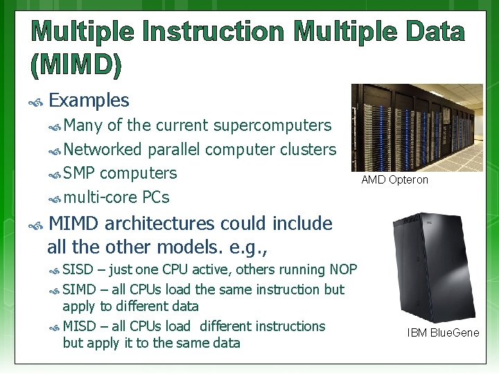
Multiple Instruction Multiple Data (MIMD) Examples Many of the current supercomputers Networked parallel computer clusters SMP computers multi-core PCs AMD Opteron MIMD architectures could include all the other models. e. g. , SISD – just one CPU active, others running NOP SIMD – all CPUs load the same instruction but apply to different data MISD – all CPUs load different instructions but apply it to the same data IBM Blue. Gene

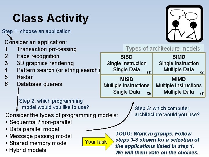
Class Activity Step 1: choose an application Consider an application: Types of architecture models 1. Transaction processing 2. Face recognition SISD SIMD Single Instruction 3. 3 D graphics rendering Single Data (1) Multiple Data (2) 4. Pattern search (or string search) 5. Radar MISD MIMD 6. Database queries Multiple Instructions Single Data Step 2: which programming model would you like to use? (3) Multiple Data Step 3: which computer architecture would you use? Consider the types of programming models: • Sequential / non-parallel • Data parallel model TODO: Work in groups. Follow • Message passing model steps 1 -3 shown for a selection of Your task • Shared memory model the applications listed in step 1. • Hybrid models We will them vote on the choices. (4)

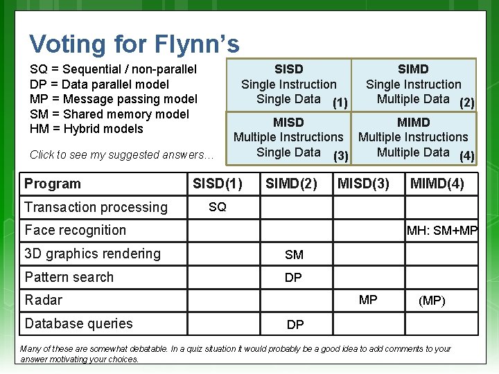
Voting for Flynn’s SISD Single Instruction Single Data (1) SQ = Sequential / non-parallel DP = Data parallel model MP = Message passing model SM = Shared memory model HM = Hybrid models Click to see my suggested answers… Program Transaction processing SIMD Single Instruction Multiple Data (2) MISD MIMD Multiple Instructions Single Data (3) Multiple Data (4) SISD(1) SIMD(2) MISD(3) SQ Face recognition MH: SM+MP 3 D graphics rendering SM Pattern search DP Radar Database queries MIMD(4) MP (MP) DP Many of these are somewhat debatable. In a quiz situation it would probably be a good idea to add comments to your answer motivating your choices.

To follow later…. EEE 4084 F Memory Architectures & Case Studies of classic microcontroller/processor architectures

EEE 4084 F Shared Memory Architecture Mine!! No! It’s mine!!

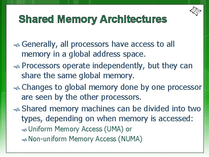
Shared Memory Architectures Generally, all processors have access to all memory in a global address space. Processors operate independently, but they can share the same global memory. Changes to global memory done by one processor are seen by the other processors. Shared memory machines can be divided into two types, depending on when memory is accessed: Uniform Memory Access (UMA) or Non-uniform Memory Access (NUMA)

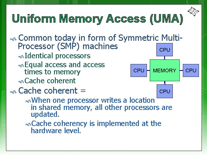
Uniform Memory Access (UMA) Common today in form of Symmetric Multi. Processor (SMP) machines CPU Identical processors Equal access and access times to memory Cache coherent = When CPU MEMORY CPU one processor writes a location in shared memory, all other processors are updated. Cache coherency is implemented at the hardware level. CPU

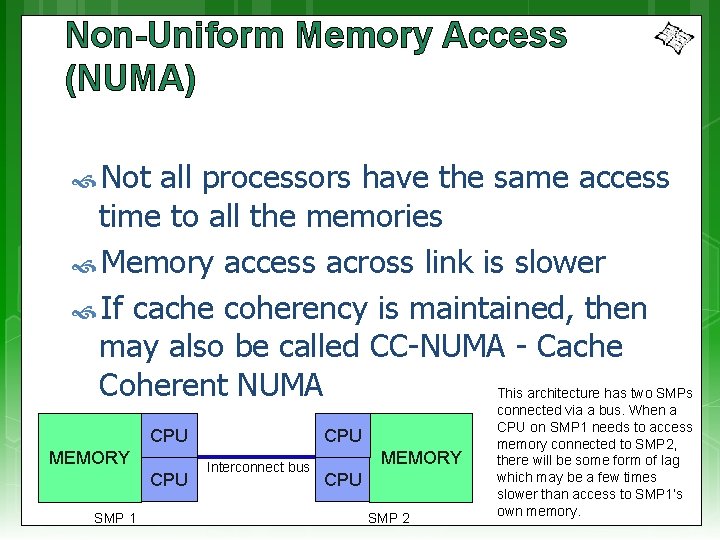
Non-Uniform Memory Access (NUMA) Not all processors have the same access time to all the memories Memory access across link is slower If cache coherency is maintained, then may also be called CC-NUMA - Cache Coherent NUMA This architecture has two SMPs CPU MEMORY CPU SMP 1 CPU Interconnect bus MEMORY CPU SMP 2 connected via a bus. When a CPU on SMP 1 needs to access memory connected to SMP 2, there will be some form of lag which may be a few times slower than access to SMP 1’s own memory.

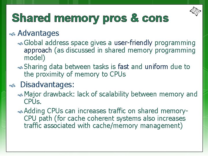
Shared memory pros & cons Advantages Global address space gives a user-friendly programming approach (as discussed in shared memory programming model) Sharing data between tasks is fast and uniform due to the proximity of memory to CPUs Disadvantages: Major drawback: lack of scalability between memory and CPUs. Adding CPUs can increases traffic on shared memory. CPU path (for cache coherent systems also increases traffic associated with cache/memory management)

Shared memory pros & cons Disadvantages Programmer responsible for implementing/using synchronization constructs to make sure that correct access of global memory is done. Becomes more difficult and expensive to design and construct shared memory machines with ever increasing numbers of processors.

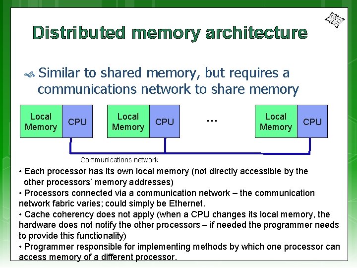
Distributed memory architecture Similar to shared memory, but requires a communications network to share memory Local Memory CPU … Local Memory CPU Communications network • Each processor has its own local memory (not directly accessible by the other processors’ memory addresses) • Processors connected via a communication network – the communication network fabric varies; could simply be Ethernet. • Cache coherency does not apply (when a CPU changes its local memory, the hardware does notify the other processors – if needed the programmer needs to provide this functionality) • Programmer responsible for implementing methods by which one processor can access memory of a different processor.

Distributed Memory architectures: Pros & Cons Advantages: Memory scalable with number of processors Each processor can access own memory quickly without communication overheads or maintaining cache coherency (for UMA). Cost benefits: use of commercial off-theshelf (COTS) processors and networks

Distributed Memory: Pros & Cons Disadvantages: Programmer takes on responsibility for data consistency, synchronization and communication between processors. Existing (legacy) programs based on shared global memory may be difficult to port to this model. May be more difficult to write applications for distributed memory systems than it is for shared memory systems. Restricted by non-uniform memory access (NUMA) performance (meaning a memory access bottle neck that may be many times slower than shared memory systems)

Distributed Shared Memory (i. e. Hybrid) System Simply a network of shared memory systems (possibly in one computer or a cluster of separated computers) Use in many modern supercomputer designs today Shared memory part is usually UMA (cache coherent) Pros & Cons? – Best and Worst of two worlds.

Thursday Pracs Thursday prac slot will be available from next week!

Intermission Next period: Considerations of reading based on shared memory and pthreads • “An architecture of on-chip-memory multi-threading processor” by T Matsuzaki, H Tomiyasu and M Amamiya • “Quantifying the Performance Impact of Memory Latency and Bandwidth for Big Data Workloads” by R Clapp, M Dimitrov, K Kumar, V Viswanathan and T Willhalm

Parallel computer memory architectures The choice of memory architecture is not necessarily dependent on the ‘Flynn classification’ For a SISM computer, this aspect is largely irrelevant (but consider a PC with GPU and DMA as not being in the SISM category)

EEE 4084 F A look at some classic microprocessor architectures Audience participation…

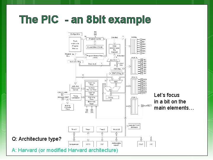
The PIC - an 8 bit example Let’s focus in a bit on the main elements… Q: Architecture type? A: Harvard (or modified Harvard architecture)

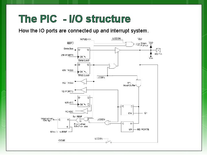
The PIC - I/O structure How the IO ports are connected up and interrupt system.

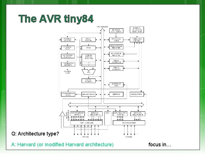
The AVR tiny 84 Q: Architecture type? A: Harvard (or modified Harvard architecture) focus in…

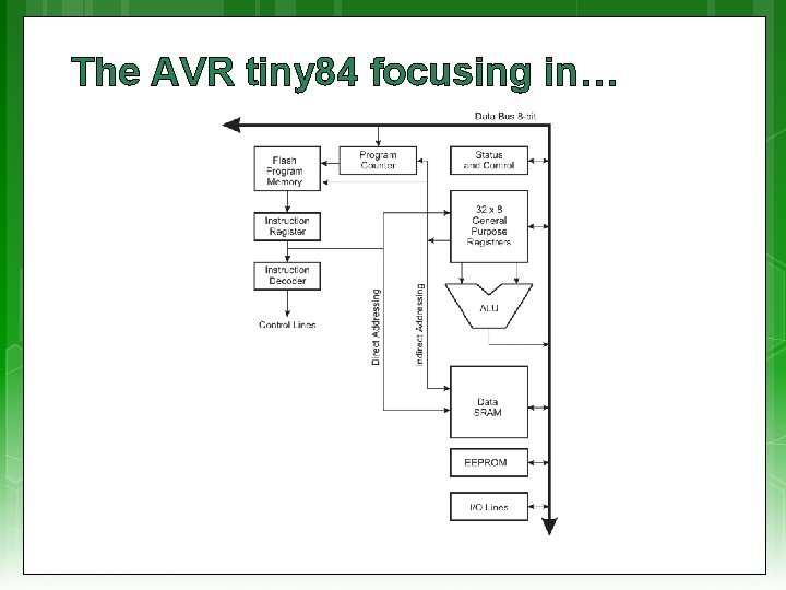
The AVR tiny 84 focusing in…

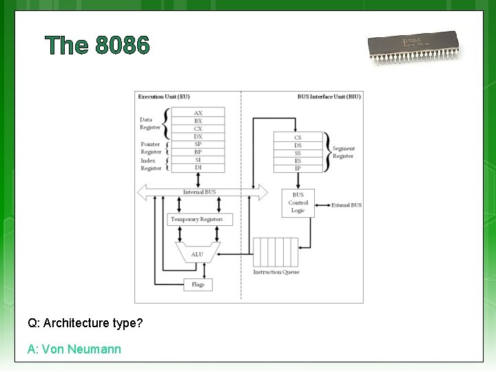
The 8086 Q: Architecture type? A: Von Neumann

EEE 4084 F Further (more complex) architecture case study

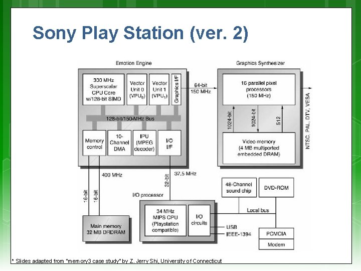
Sony Play Station (ver. 2) * Slides adapted from “memory 3 case study” by Z. Jerry Shi, University of Connecticut

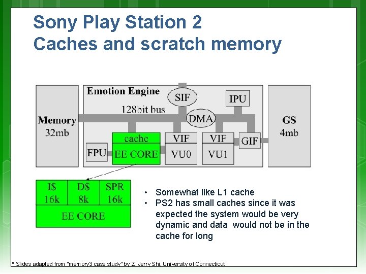
Sony Play Station 2 Caches and scratch memory • Somewhat like L 1 cache • PS 2 has small caches since it was expected the system would be very dynamic and data would not be in the cache for long * Slides adapted from “memory 3 case study” by Z. Jerry Shi, University of Connecticut

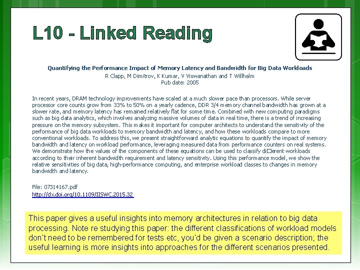
L 10 - Linked Reading Quantifying the Performance Impact of Memory Latency and Bandwidth for Big Data Workloads R Clapp, M Dimitrov, K Kumar, V Viswanathan and T Willhalm Pub date: 2005 In recent years, DRAM technology improvements have scaled at a much slower pace than processors. While server processor core counts grow from 33% to 50% on a yearly cadence, DDR 3/4 memory channel bandwidth has grown at a slower rate, and memory latency has remained relatively flat for some time. Combined with new computing paradigms such as big data analytics, which involves analyzing massive volumes of data in real time, there is a trend of increasing pressure on the memory subsystem. This makes it important for computer architects to understand the sensitivity of the performance of big data workloads to memory bandwidth and latency, and how these workloads compare to more conventional workloads. To address this, we present straightforward analytic equations to quantify the impact of memory bandwidth and latency on workload performance, leveraging measured data from performance counters on real systems. We demonstrate how the values of the components of these equations can be used to classify di�erent workloads according to their inherent bandwidth requirement and latency sensitivity. Using this performance model, we show the relative sensitivities of big data, high-performance computing, and enterprise workload classes to changes in memory bandwidth and latency. File: 07314167. pdf http: //dx. doi. org/10. 1109/IISWC. 2015. 32 This paper gives a useful insights into memory architectures in relation to big data processing. Note re studying this paper: the different classifications of workload models don’t need to be remembered for tests etc, you’d be given a scenario description; the useful learning is more insights into approaches for the different scenarios presented.

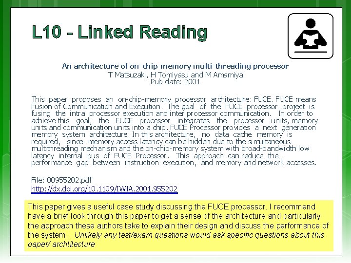
L 10 - Linked Reading An architecture of on-chip-memory multi-threading processor T Matsuzaki, H Tomiyasu and M Amamiya Pub date: 2001 This paper proposes an on-chip-memory processor architecture: FUCE means Fusion of Communication and Execution. The goal of the FUCE processor project is fusing the intra processor execution and inter processor communication. In order to achieve this goal, the FUCE processor integrates the processor units, memory units and communication units into a chip. FUCE Processor provides a next generation memory system architecture. In this architecture, no data cache memory is required, since memory access latency can be hidden due to the simultaneous multithreading mechanism and the on-chip-memory system with broad-bandwidth low latency internal bus of FUCE Processor. This approach can reduce the performance gap between instruction execution, and memory and network accesses. File: 00955202. pdf http: //dx. doi. org/10. 1109/IWIA. 2001. 955202 This paper gives a useful case study discussing the FUCE processor. I recommend have a brief look through this paper to get a sense of the architecture and particularly the approach these authors take to explain their design and discuss the performance of the system. Unlikely any test/exam questions would ask specific questions about this paper/ archtitecture

Disclaimers and copyright/licensing details I have tried to follow the correct practices concerning copyright and licensing of material, particularly image sources that have been used in this presentation. I have put much effort into trying to make this material open access so that it can be of benefit to others in their teaching and learning practice. Any mistakes or omissions with regards to these issues I will correct when notified. To the best of my understanding the material in these slides can be shared according to the Creative Commons “Attribution-Share. Alike 4. 0 International (CC BY-SA 4. 0)” license, and that is why I selected that license to apply to this presentation (it’s not because I particulate want my slides referenced but more to acknowledge the sources and generosity of others who have provided free material such as the images I have used). Image sources: Stop watch slides 1 & 14, Gold bar: Wikipedia (open commons) books clipart: http: //www. clker. com (open commons) computer motherboard - Wikipedia (open commons) various clipart - Pixabay