EEE 4084 F Digital Systems Lecture 17 RC
![The Cell Processor Milestones 2005 Feb [1, 2] IBM’s technical disclosures of cell processors The Cell Processor Milestones 2005 Feb [1, 2] IBM’s technical disclosures of cell processors](https://slidetodoc.com/presentation_image_h/0dc507cc54c1a82cd66c84c537281665/image-5.jpg)

- Slides: 29

EEE 4084 F Digital Systems Lecture 17 RC Architectures Case Studies Microprocessor-based: Cell Broadband Engine Architecture FPGA-based: PAM, VCC, SPLASH … Lecturer: Simon Winberg Attribution-Share. Alike 4. 0 International (CC BY-SA 4. 0)

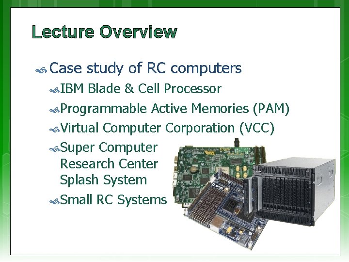
Lecture Overview Case study of RC computers IBM Blade & Cell Processor Programmable Active Memories (PAM) Virtual Computer Corporation (VCC) Super Computer Research Center Splash System Small RC Systems

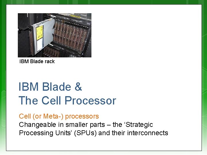
CASE STUDY: IBM Blade rack IBM Blade & The Cell Processor Cell (or Meta-) processors Changeable in smaller parts – the ‘Strategic Processing Units’ (SPUs) and their interconnects

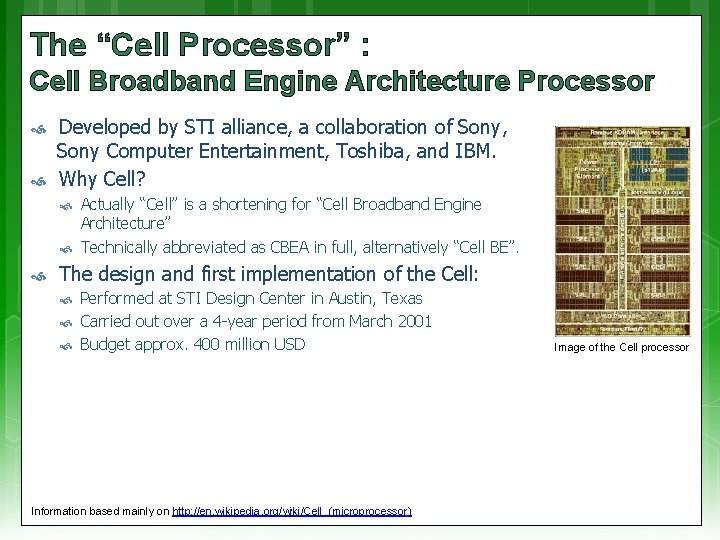
The “Cell Processor” : Cell Broadband Engine Architecture Processor Developed by STI alliance, a collaboration of Sony, Sony Computer Entertainment, Toshiba, and IBM. Why Cell? Actually “Cell” is a shortening for “Cell Broadband Engine Architecture” Technically abbreviated as CBEA in full, alternatively “Cell BE”. The design and first implementation of the Cell: Performed at STI Design Center in Austin, Texas Carried out over a 4 -year period from March 2001 Budget approx. 400 million USD Information based mainly on http: //en. wikipedia. org/wiki/Cell_(microprocessor) Image of the Cell processor
![The Cell Processor Milestones 2005 Feb 1 2 IBMs technical disclosures of cell processors The Cell Processor Milestones 2005 Feb [1, 2] IBM’s technical disclosures of cell processors](https://slidetodoc.com/presentation_image_h/0dc507cc54c1a82cd66c84c537281665/image-5.jpg)
The Cell Processor Milestones 2005 Feb [1, 2] IBM’s technical disclosures of cell processors quickly led to new platforms & toolsets [2] Oct 05: Mercury Cell Blade Nov 05: Open Source SDK & Simulator Feb 06: IBM Cell Blade Resources / further reading http: //www-128. ibm. com/developerworks/power/cell/ http: //www. research. ibm. com/cell/ (see copy of condensed article: Lect 17 - The Cell architecture. pdf) [1] IBM press release 7 -Feb-2005: http: //www-03. ibm. com/press/us/en/pressrelease/7502. wss [2] http: //www. scei. co. jp/corporate/release/pdf/051110 e. pdf

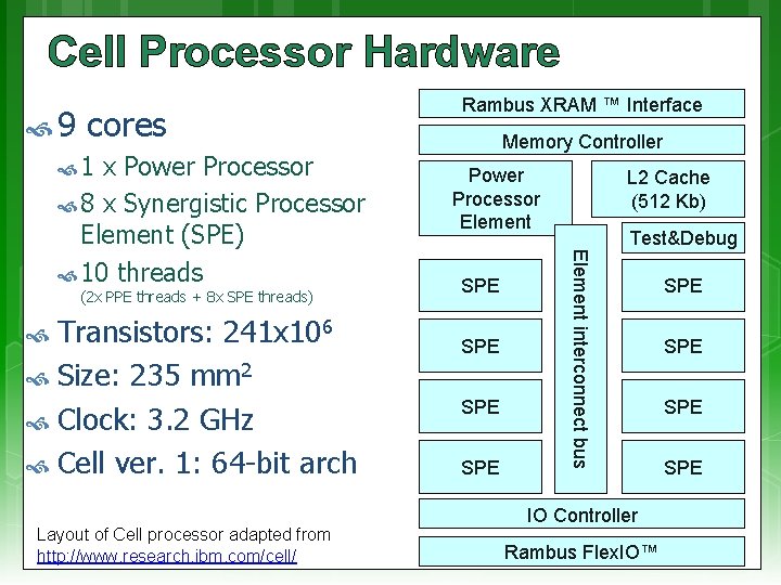
Cell Processor Hardware (2 x PPE threads + 8 x SPE threads) Transistors: 241 x 106 Size: 235 mm 2 Clock: 3. 2 GHz Cell ver. 1: 64 -bit arch Layout of Cell processor adapted from http: //www. research. ibm. com/cell/ Memory Controller Power Processor Element SPE SPE L 2 Cache (512 Kb) Test&Debug Element interconnect bus 9 cores 1 x Power Processor 8 x Synergistic Processor Element (SPE) 10 threads Rambus XRAM ™ Interface IO Controller Rambus Flex. IO™ SPE SPE

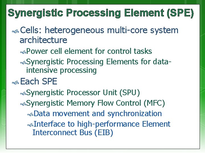
Synergistic Processing Element (SPE) Cells: heterogeneous multi-core system architecture Power cell element for control tasks Synergistic Processing Elements for data- intensive processing Each SPE Synergistic Processor Unit (SPU) Synergistic Memory Flow Control (MFC) Data movement and synchronization Interface to high-performance Element Interconnect Bus (EIB)

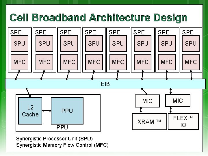
Cell Broadband Architecture Design SPE SPE SPU SPU MFC MFC EIB L 2 Cache MIC PPU Synergistic Processor Unit (SPU) Synergistic Memory Flow Control (MFC) XRAM ™ FLEX™ IO

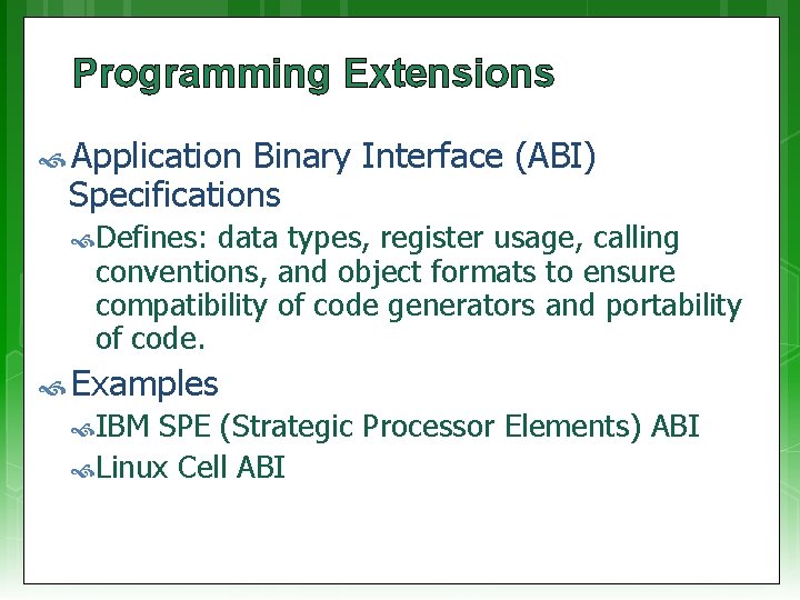
Programming Extensions Application Binary Interface (ABI) Specifications Defines: data types, register usage, calling conventions, and object formats to ensure compatibility of code generators and portability of code. Examples IBM SPE (Strategic Processor Elements) ABI Linux Cell ABI

IBM SPE for Cell Processors SPE C/C++ Language Extensions Defines: standardized data types, compiler directives, and language extensions used to make use of SIMD capabilities in the core

Cell Processor Programming Models Reconfigurable Computing

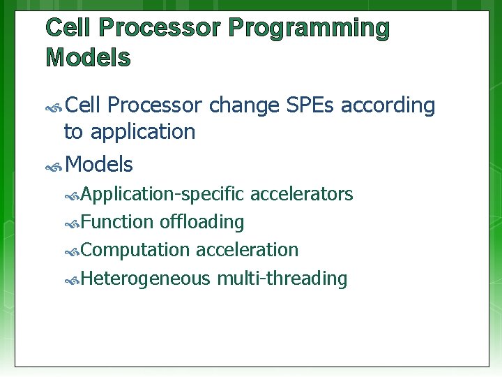
Cell Processor Programming Models Cell Processor change SPEs according to application Models Application-specific accelerators Function offloading Computation acceleration Heterogeneous multi-threading

Application Specific Accelerators Example 3 D Visualization Application Software Hardware FLEX™ IO PPE DATA Stores EIB SPE 1 SPE 2 3 D Graphics Acceleration Software SPE 3 Texture mapping SPE 4 Data decomp ression SPE 5 SPE 6 SPE 7 Data comparison and classification SPE 8 3 D Scene Generation

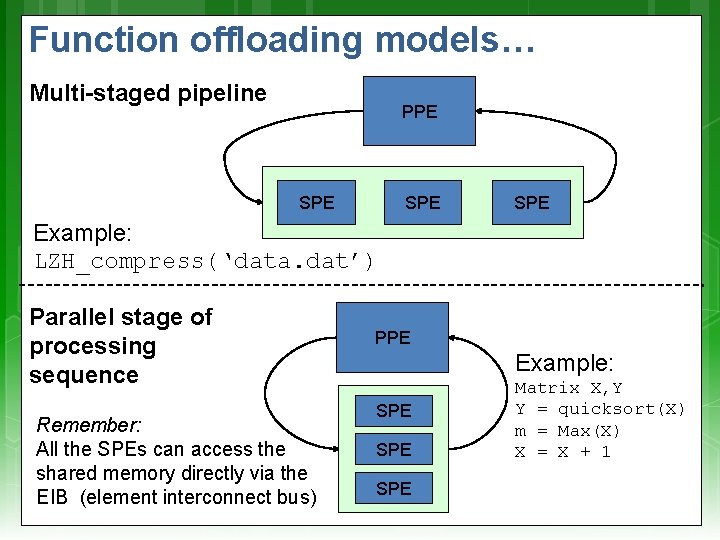
Function offloading models… Multi-staged pipeline PPE SPE SPE Example: LZH_compress(‘data. dat’) Parallel stage of processing sequence Remember: All the SPEs can access the shared memory directly via the EIB (element interconnect bus) PPE Example: SPE SPE Matrix X, Y Y = quicksort(X) m = Max(X) X = X + 1

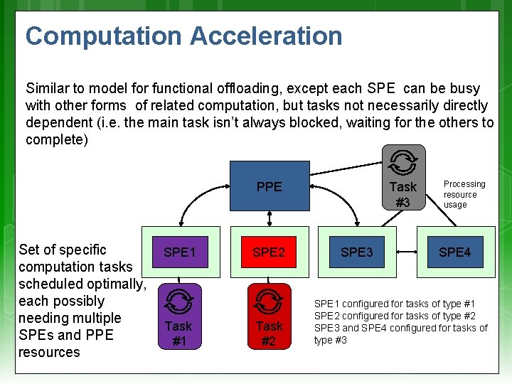
Computation Acceleration Similar to model for functional offloading, except each SPE can be busy with other forms of related computation, but tasks not necessarily directly dependent (i. e. the main task isn’t always blocked, waiting for the others to complete) PPE Set of specific computation tasks scheduled optimally, each possibly needing multiple SPEs and PPE resources SPE 1 Task #1 SPE 2 Task #3 SPE 3 Processing resource usage SPE 4 SPE 1 configured for tasks of type #1 SPE 2 configured for tasks of type #2 SPE 3 and SPE 4 configured for tasks of type #3

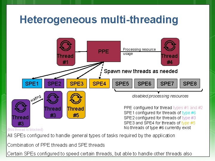
Heterogeneous multi-threading Thread #1 PPE Processing resource usage Thread #4 Spawn new threads as needed SPE 1 SPE 2 SPE 3 SPE 4 SPE 6 SPE 7 SPE 8 disabled processing resources g itin wa Thread #3 SPE 5 Thread #3 Thread #5 (this thread is blocked) PPE configured for thread types #1 and #2 SPE 1 configured for threads of type #6 SPE 2 configured for threads of type #3 SPE 3 and SPE 4 for threads of type #5 No threads of type #6 currently exist All SPEs configured to handle general types of tasks required by the application Combination of PPE threads and SPE threads Certain SPEs configured to speed certain threads, but able to handle other threads also

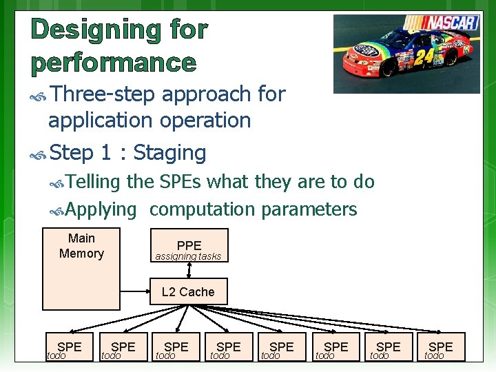
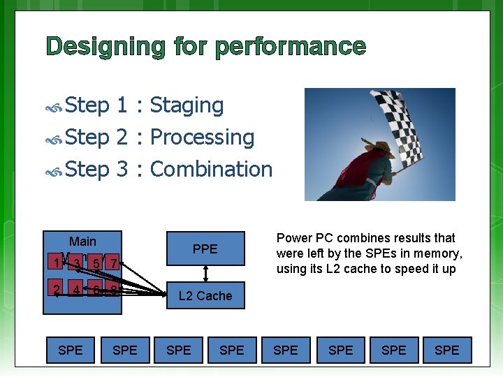
Designing for performance Three-step approach for application operation Step 1 : Staging Telling the SPEs what they are to do Applying computation parameters Main Memory PPE assigning tasks L 2 Cache SPE todo SPE todo

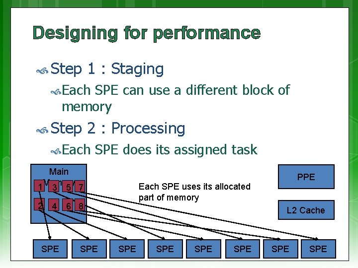
Designing for performance Step 1 : Staging Each SPE can use a different block of memory Step 2 : Processing Each SPE does its assigned task Main Memory 1 3 5 7 2 Each SPE uses its allocated part of memory 4 6 8 SPE PPE L 2 Cache SPE SPE SPE

Designing for performance Step 1 : Staging Step 2 : Processing Step 3 : Combination Main Memory 1 3 5 7 2 4 6 8 SPE Power PC combines results that were left by the SPEs in memory, using its L 2 cache to speed it up PPE L 2 Cache SPE SPE SPE

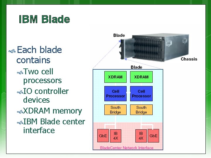
IBM Blade Each blade contains Two cell processors IO controller devices XDRAM memory IBM Blade center interface

RC Systems A look at platforms architectures

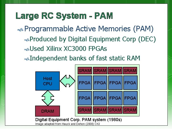
Large RC System - PAM Programmable Active Memories (PAM) Produced by Digital Equipment Corp (DEC) Used Xilinx XC 3000 FPGAs Independent banks of fast static RAM SRAM Host CPU FPGA FPGA DRAM SRAM Digital Equipment Corp. PAM system (1980 s) Image adapted from Hauck and Dehon (2008) Ch 3

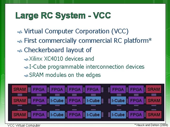
Large RC System - VCC Virtual Computer Corporation (VCC) First commercially commercial RC platform* Checkerboard layout of Xilinx XC 4010 devices and I-Cube programmable interconnection devices SRAM modules on the edges SRAM FPGA … FPGA SRAM … FPGA … I-Cube … FPGA … SRAM FPGA I-Cube … I-Cube FPGA SRAM VCC Virtual Computer * Hauck and Dehon (2008)

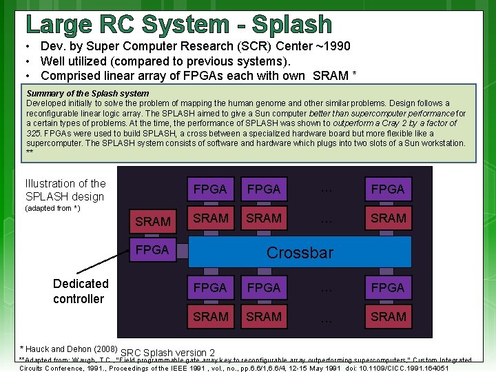
Large RC System - Splash • Dev. by Super Computer Research (SCR) Center ~1990 • Well utilized (compared to previous systems). • Comprised linear array of FPGAs each with own SRAM * Summary of the Splash system Developed initially to solve the problem of mapping the human genome and other similar problems. Design follows a reconfigurable linear logic array. The SPLASH aimed to give a Sun computer better than supercomputer performance for a certain types of problems. At the time, the performance of SPLASH was shown to outperform a Cray 2 by a factor of 325. FPGAs were used to build SPLASH, a cross between a specialized hardware board but more flexible like a supercomputer. The SPLASH system consists of software and hardware which plugs into two slots of a Sun workstation. ** Illustration of the SPLASH design (adapted from *) SRAM FPGA … FPGA SRAM … SRAM FPGA Dedicated controller * Hauck and Dehon (2008) Crossbar FPGA … FPGA SRAM … SRAM SRC Splash version 2 **Adapted from: Waugh, T. C. , "Field programmable gate array key to reconfigurable array outperforming supercomputers, " Custom Integrated Circuits Conference, 1991. , Proceedings of the IEEE 1991 , vol. , no. , pp. 6. 6/1, 6. 6/4, 12 -15 May 1991 doi: 10. 1109/CICC. 1991. 164051

Small RC Systems Brown University’s PRISM Single FPGA co-processor in each computer in a cluster Main CPUs offloading parallelized functions to FPGA Algotronix Configurable Array Logic (CAL) – FPGA featuring very simple logic cells (compared to other FPGAs) Later become XC 6200 (when CAL bought by Xilinx) * Hauck and Dehon (2008)

Reconfigurable Supercomputers Cray Research XD 1: 12 processing nodes 6 x ADM Opteron processors 6 x Reconfigurable nodes built from Xilinx Vertex 4 Each XD 1 in own chassis, can connect up to 12 chassis in a cabined (i. e. 144 processing nodes) SRC Traditional processor + reconfig. processing unit Based on Xilinx Virtex FPGAs Silicon Graphics RASP (reconfigurable application-specific processor) Blade-type approach of smaller boards plugging into larger ones Ref: Hauck and Dehon Ch 3 (2008)

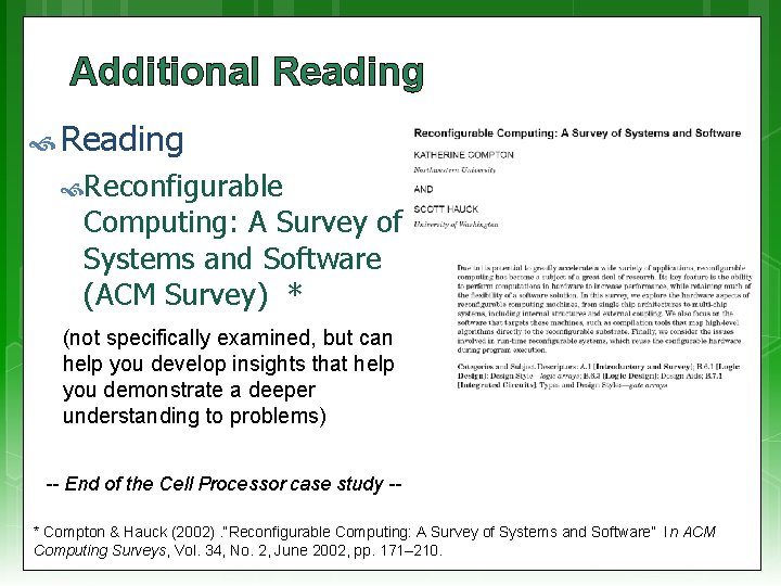
Additional Reading Reconfigurable Computing: A Survey of Systems and Software (ACM Survey) * (not specifically examined, but can help you develop insights that help you demonstrate a deeper understanding to problems) -- End of the Cell Processor case study -* Compton & Hauck (2002). “Reconfigurable Computing: A Survey of Systems and Software” In ACM Computing Surveys, Vol. 34, No. 2, June 2002, pp. 171– 210.

Conclusion & Plans Reading Hauck, Scott (1998). “The Roles of FPGAs in Reprogrammable Systems” In Proceedings of the IEEE. 86(4) pp. 615 -639. Next lecture: Amdahl’s Law Discussion of YODA phase 1

Disclaimers and copyright/licensing details I have tried to follow the correct practices concerning copyright and licensing of material, particularly image sources that have been used in this presentation. I have put much effort into trying to make this material open access so that it can be of benefit to others in their teaching and learning practice. Any mistakes or omissions with regards to these issues I will correct when notified. To the best of my understanding the material in these slides can be shared according to the Creative Commons “Attribution-Share. Alike 4. 0 International (CC BY-SA 4. 0)” license, and that is why I selected that license to apply to this presentation (it’s not because I particulate want my slides referenced but more to acknowledge the sources and generosity of others who have provided free material such as the images I have used). Image sources: IBM Blade rack (slide 3), IBM blade, Checkered flag – Wikipedia open commons NASCAR image – flickr CC 2 share alike