1 2 Semiconductor and PN junction EEE 270


 18 EEE 270 Electronic engineering")
 19 EEE 270 Electronic engineering")


- Slides: 38
บทท 1 2 Semiconductor and P-N junction EEE 270 Electronic engineering
Semiconductor material Silicon wafer 2 EEE 270 Electronic engineering
Semiconductor material Silicon crystal Sand 25% silicon 3 EEE 270 Electronic engineering
Semiconductor material 4 EEE 270 Electronic engineering
Silicon atom 5 EEE 270 Electronic engineering
Intrinsic semiconductor Silicon Crystal at T= 0 °K 6 EEE 270 Electronic engineering
Energy gap 7 EEE 270 Electronic engineering
Energy level An electron-volt is the energy of an electron that has been accelerated through a potential difference of 1 volt, and 1 e. V= 1. 6*10 -19 joules 8 EEE 270 Electronic engineering
Intrinsic semiconductor Silicon Crystal at T > 0 °K 9 EEE 270 Electronic engineering
The Intrinsic Carrier Concentration ni B Eg T k 10 is the intrinsic carrier concentration is a constant related to the specific semiconductor material is the band-gap energy (e. V) is the temperature (°K) is Boltzmann’s constant (86 x 10 -6 e. V/°K) EEE 270 Electronic engineering
Electrical current 11 EEE 270 Electronic engineering
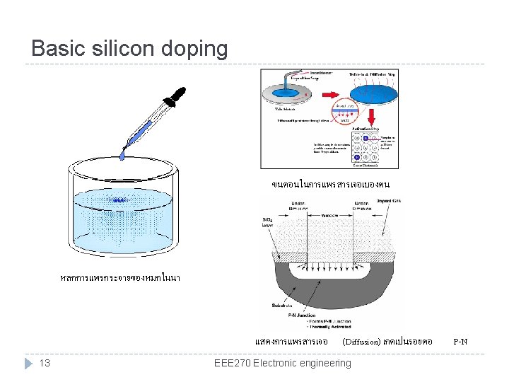
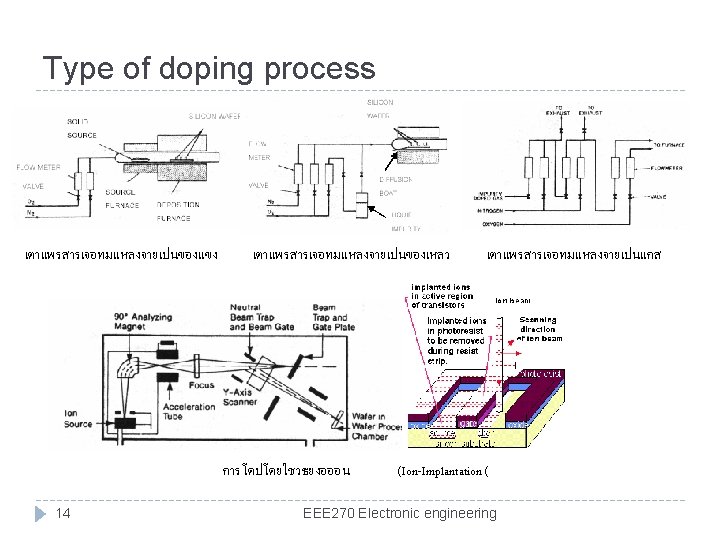
Doping and Extrinsic Semiconductors 12 EEE 270 Electronic engineering
N-type semiconductor 15 EEE 270 Electronic engineering
P-type semiconductor 16 EEE 270 Electronic engineering
Thermal equilibrium no = thermal equilibrium concentration of free electron po = thermal equilibrium concentration of hole Silicon Crystal at T > 0 °K 17 EEE 270 Electronic engineering
Thermal equilibrium (N-type) 18 EEE 270 Electronic engineering
Thermal equilibrium (P-type) 19 EEE 270 Electronic engineering
Drift and Diffusion Currents 20 EEE 270 Electronic engineering
Drift and Diffusion Currents 21 EEE 270 Electronic engineering
Drift and Diffusion Currents 22 EEE 270 Electronic engineering
Drift and Diffusion Currents 23 EEE 270 Electronic engineering
Drift and Diffusion Currents 24 EEE 270 Electronic engineering
Drift and Diffusion Currents 25 EEE 270 Electronic engineering
Drift and Diffusion Currents 26 EEE 270 Electronic engineering
Drift and Diffusion Currents 27 EEE 270 Electronic engineering
P-N junction Bell Labs the first transistor in December 1947. 28 EEE 270 Electronic engineering
P-N Junction 29 EEE 270 Electronic engineering
The Equilibrium P-N Junction 30 EEE 270 Electronic engineering
The Equilibrium P-N Junction Barrier potential or Built-in voltage is called thermal voltage, approximately 0. 026 V at room temperature, T=300 °K 31 EEE 270 Electronic engineering
Built-in voltage 32 EEE 270 Electronic engineering
P-N Junction biasing Forward-bias Non-bias Reward-bias 33 EEE 270 Electronic engineering
P-N Junction biasing 34 EEE 270 Electronic engineering
Junction capacitance 35 EEE 270 Electronic engineering
Reverse-Biased P-N Junction Reward-bias Cj : Junction Capacitance Cj 0 : Junction Capacitance at zero applied voltage VR : Reverse bias voltage Vbi : built-in voltage 36 EEE 270 Electronic engineering
Forward-Biased P-N Junction Forward-bias IS : Reverse-bias Saturation current, in the range of 10 -15 to 10 -13 VT : Thermal voltage n : emission coefficient or ideality factor, in the range 1 n 2 37 EEE 270 Electronic engineering
Forward-Biased P-N Junction 38 EEE 270 Electronic engineering