Lecture01 EE 4109 Dept of EEE KUET This
- Slides: 28

Lecture-01 EE 4109 Dept. of EEE, KUET

This lecture is for Learning Outcome 3 (LO 3): At the end of the course students will be able to identify and design DC-AC converters (inverters) and their gate driver circuits q Basic of inverter q Principle of operation of inverters q Performance parameters of inverters

Inverter basic DC to AC converters are known as inverters The function of an inverter is to change a dc input voltage to a symmetric ac output voltage of desired magnitude and frequency The output voltage could be fixed or variable at a fixed or variable frequency. Variable output voltage can be obtained by varying the gain of the inverter.

Inverter basic Inverter gain= ac output/dc input (which is controlled by using PWM) Applications: variable speed ac motor, induction heating, IPS, and UPS Classification: single-phase and three-phase

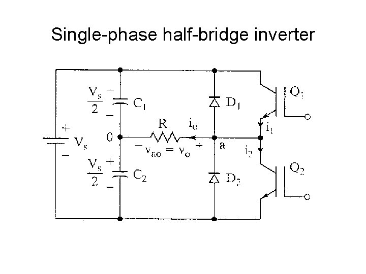
Single-phase half-bridge inverter

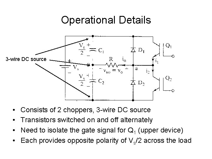
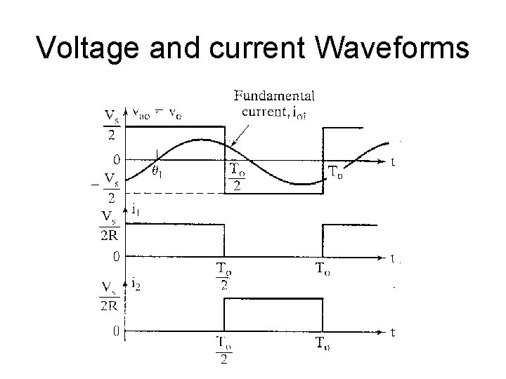
Operational Details 3 -wire DC source • • Consists of 2 choppers, 3 -wire DC source Transistors switched on and off alternately Need to isolate the gate signal for Q 1 (upper device) Each provides opposite polarity of Vs/2 across the load

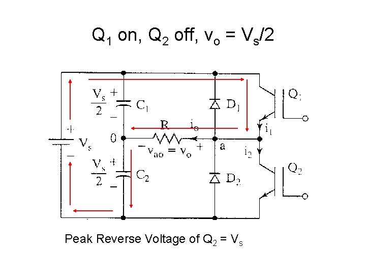
Q 1 on, Q 2 off, vo = Vs/2 Peak Reverse Voltage of Q 2 = Vs

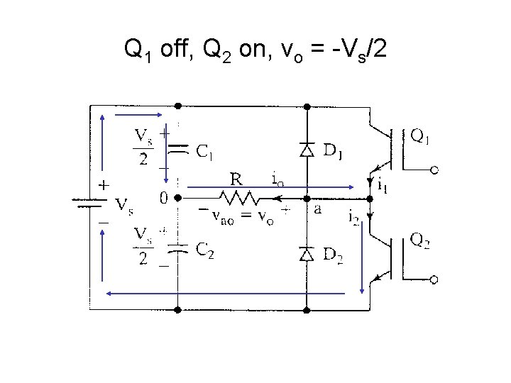
Q 1 off, Q 2 on, vo = -Vs/2

Voltage and current Waveforms

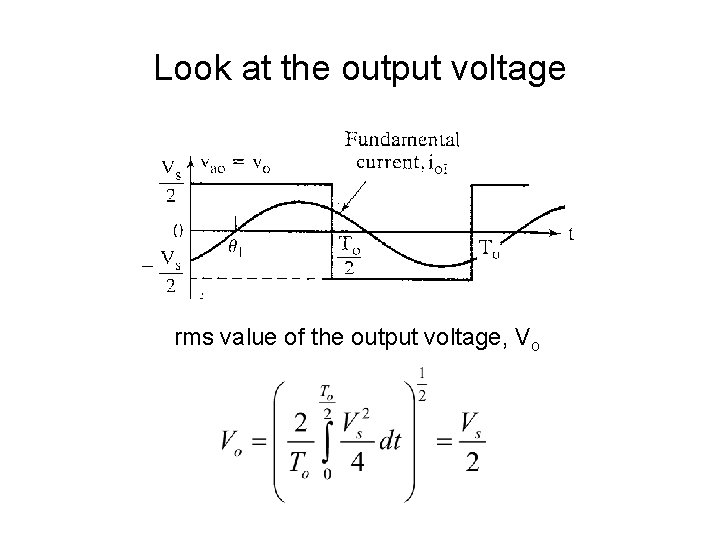
Look at the output voltage rms value of the output voltage, Vo

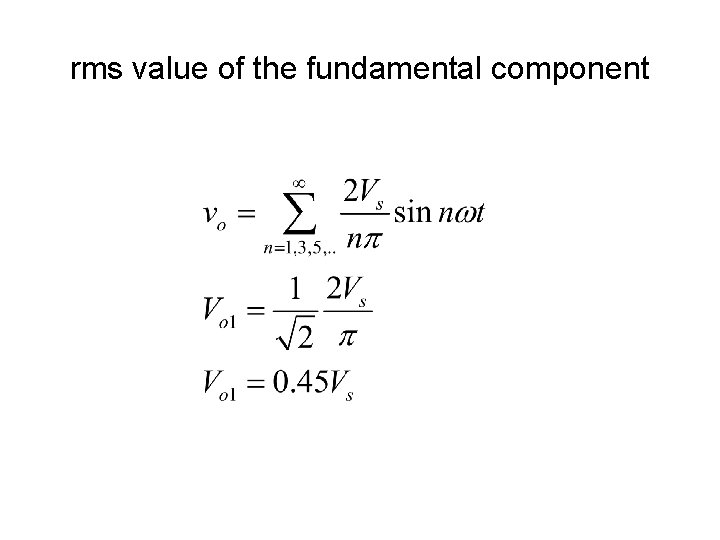
rms value of the fundamental component

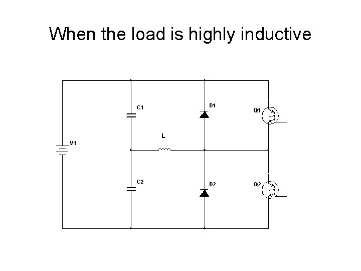
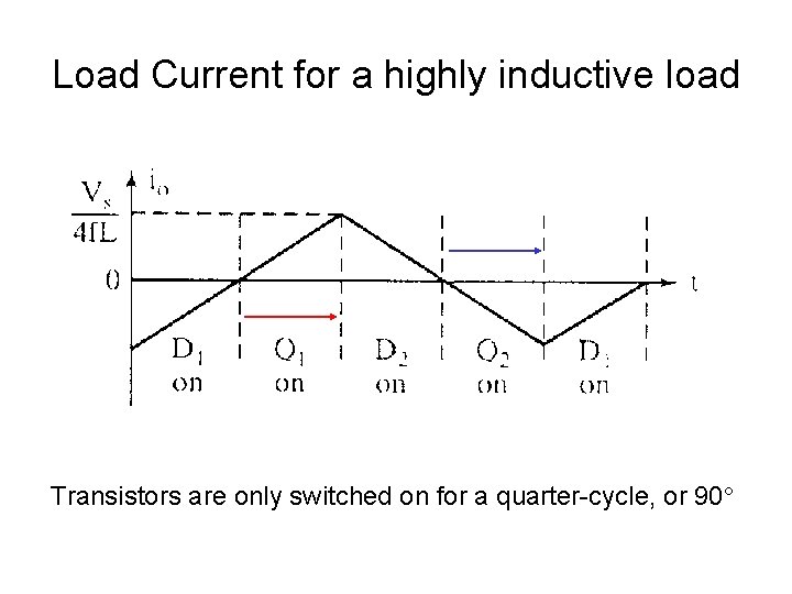
When the load is highly inductive

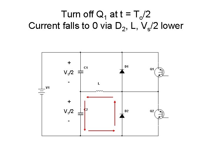
Turn off Q 1 at t = To/2 Current falls to 0 via D 2, L, Vs/2 lower + Vs/2 -

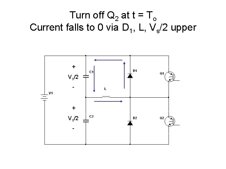
Turn off Q 2 at t = To Current falls to 0 via D 1, L, Vs/2 upper + Vs/2 -

Load Current for a highly inductive load Transistors are only switched on for a quarter-cycle, or 90

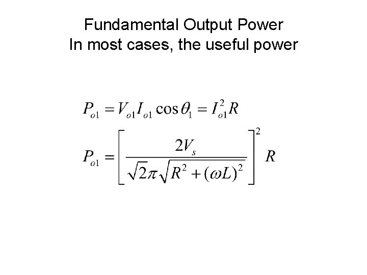
Fundamental Output Power In most cases, the useful power

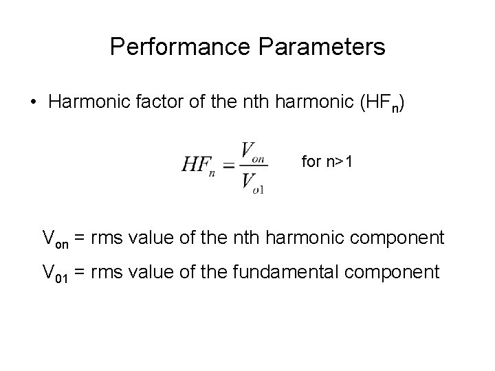
Performance Parameters • Harmonic factor of the nth harmonic (HFn) for n>1 Von = rms value of the nth harmonic component V 01 = rms value of the fundamental component

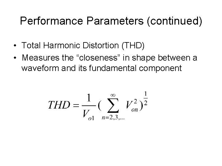
Performance Parameters (continued) • Total Harmonic Distortion (THD) • Measures the “closeness” in shape between a waveform and its fundamental component

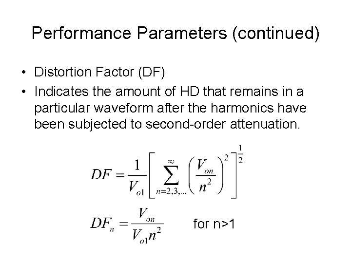
Performance Parameters (continued) • Distortion Factor (DF) • Indicates the amount of HD that remains in a particular waveform after the harmonics have been subjected to second-order attenuation. for n>1

Performance Parameters (continued) • Lowest order harmonic (LOH) • The harmonic component whose frequency is closest to the fundamental, and its amplitude is greater than or equal to 3% of the amplitude of the fundamental component.

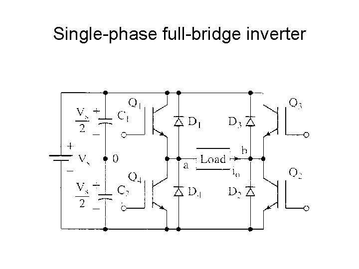
Single-phase full-bridge inverter

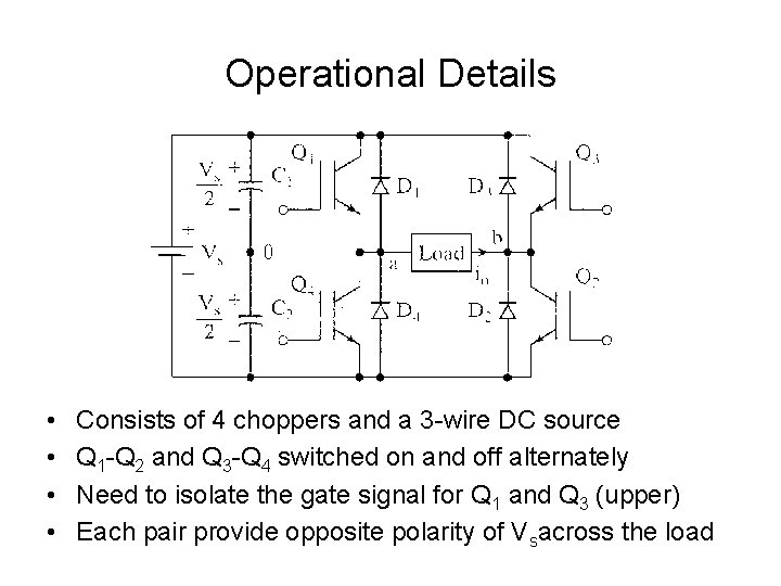
Operational Details • • Consists of 4 choppers and a 3 -wire DC source Q 1 -Q 2 and Q 3 -Q 4 switched on and off alternately Need to isolate the gate signal for Q 1 and Q 3 (upper) Each pair provide opposite polarity of Vsacross the load

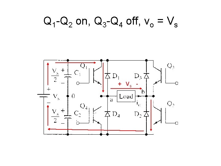
Q 1 -Q 2 on, Q 3 -Q 4 off, vo = Vs + Vs -

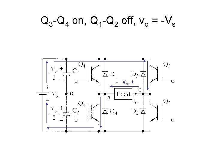
Q 3 -Q 4 on, Q 1 -Q 2 off, vo = -Vs - Vs +

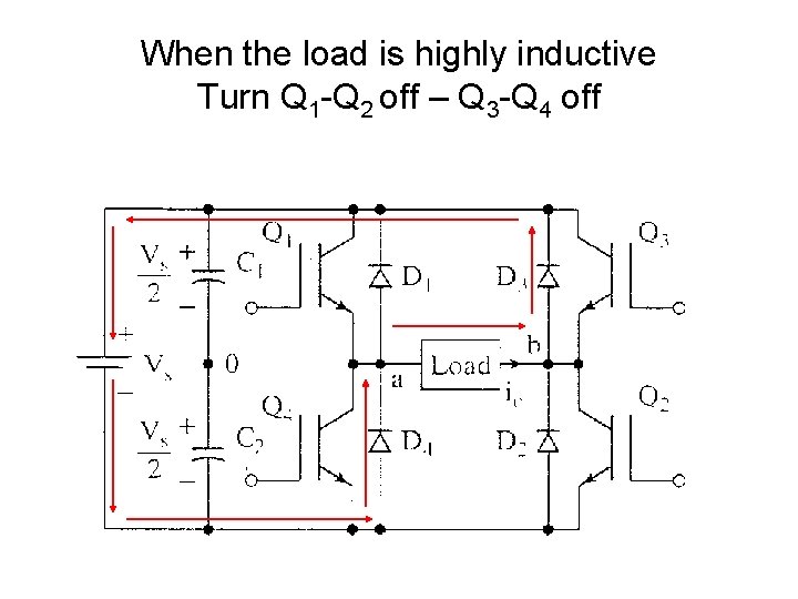
When the load is highly inductive Turn Q 1 -Q 2 off – Q 3 -Q 4 off

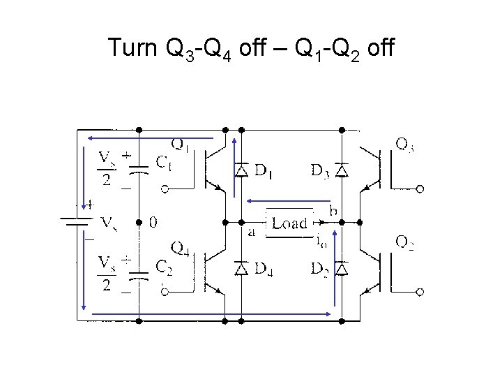
Turn Q 3 -Q 4 off – Q 1 -Q 2 off

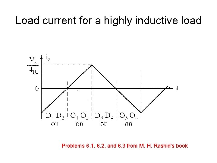
Load current for a highly inductive load Problems 6. 1, 6. 2, and 6. 3 from M. H. Rashid’s book

End of Lecture 1