EECS 150 Spring 2008 Checkpoint 1 SDRAM 2292008
- Slides: 22

EECS 150 Spring 2008 Checkpoint 1 - SDRAM 2/29/2008 Chen Sun (Adapted From Slides by Greg Gibeling)

Welcome to Checkpoint 1 n Agenda n n n Why Checkpoint 1 is Important Checkpoint 1 Specs Theory of SDRAM Init, Read, Write (timing diagrams) Designing the SDRAM controller

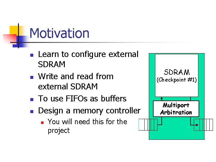
Motivation n n Learn to configure external SDRAM Write and read from external SDRAM To use FIFOs as buffers Design a memory controller n You will need this for the project SDRAM (Checkpoint #1) Multiport Arbitration

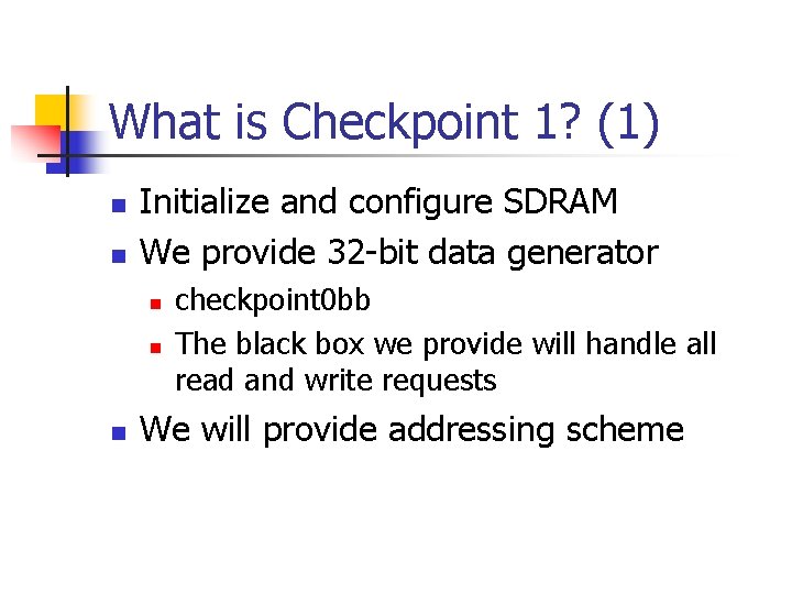
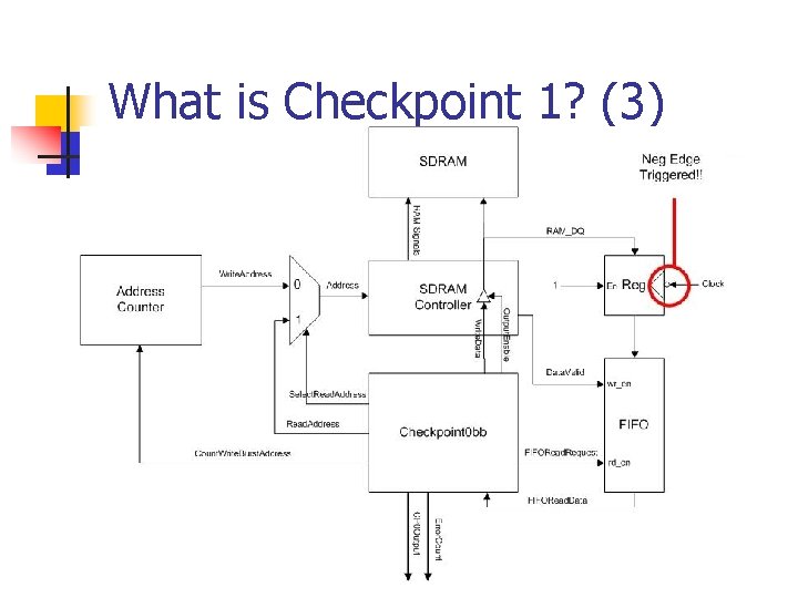
What is Checkpoint 1? (1) n n Initialize and configure SDRAM We provide 32 -bit data generator n n n checkpoint 0 bb The black box we provide will handle all read and write requests We will provide addressing scheme

What is Checkpoint 1 (2) n n We provide data checker to compare what is read from SDRAM from what should have been written Count the errors and display on LEDs

What is Checkpoint 1? (3)

Theory of SDRAM (1) n SDRAM: Synchronous Dynamic RAM n Upside n n Huge amounts of storage Down side n n Slow May need refreshing every once in a while

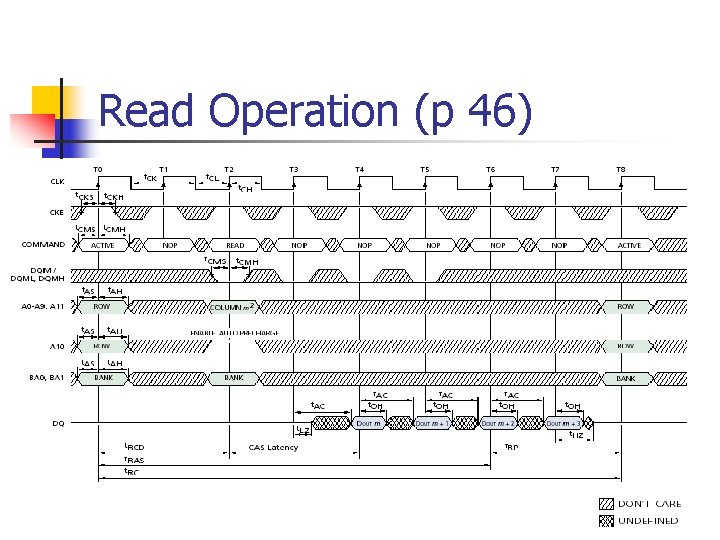
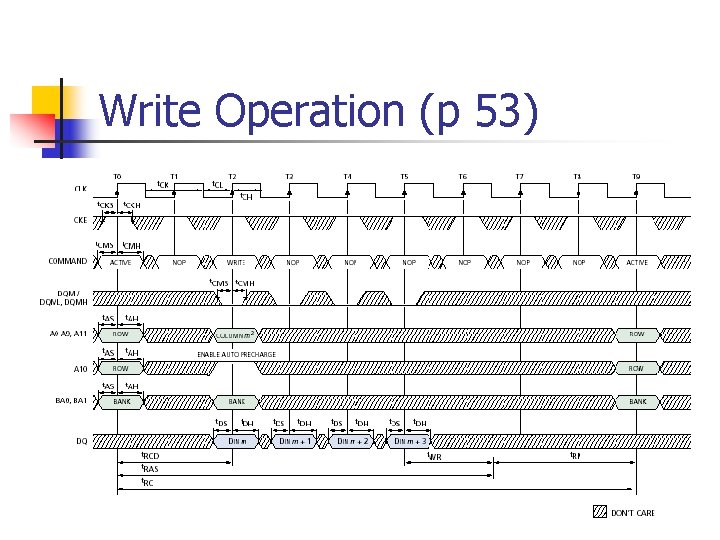
Theory of SDRAM (2) n So to speed things up… n SDRAM handles bursts to read data as a group n n n Control requires precise timing Issue sequences of commands Timing must be matched with Data Sheet (more on this later)

Theory of SDRAM (3) n DRAM is BIG so we time mux address n n n Steps to Read/Write n n Row Address Column Address Send Row Address Send Column Address Send/Get Data Read the Data sheet for details

Theory of SDRAM (4) n SDRAM is a large FSM n n n Send it a command Get a response SDRAM Controller’s Job: n n Send the right command signals Ensure command sequences are timed correctly

SDRAM Specifications n See Spec at n n http: //wwwinst. eecs. berkeley. edu/~cs 150/sp 07/Documents. p hp#Datasheets Read the MT 48 LC 16 M 16 Datasheet Provides overview of commands and timing You will need to become very familiar with initialization, reads, and writes

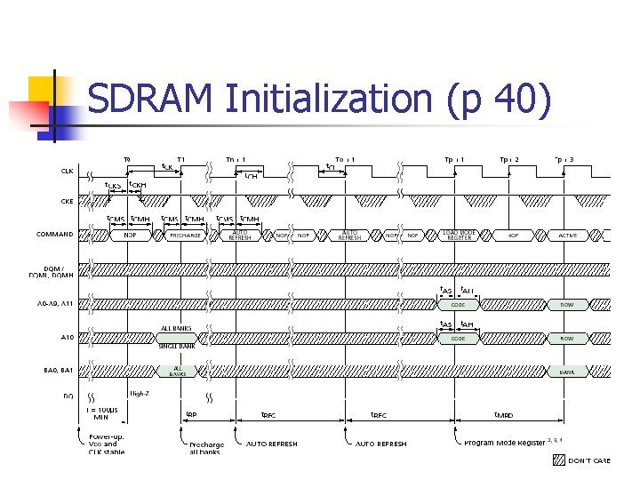
SDRAM Initialization (p 40)

Read Operation (p 46)

Write Operation (p 53)

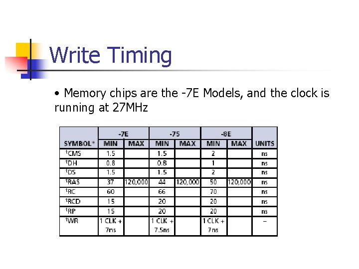
Write Timing • Memory chips are the -7 E Models, and the clock is running at 27 MHz

SDRAM Controller (1) n One Time n n Initialization Repeating n n n Read with auto-precharge Write with auto-precharge Auto-Refresh (only if idle for a long time) n Refreshes should not be necessary for this project

SDRAM Controller (2) n Goal n n Abstracts away the details of SDRAM Accepts commands, produces responses Deals with sending address in parts (row and then column) Design Options n Completely up to you!

SDRAM Controller (3) n n Design for the future! You will need it for your project Tristate data line when reading! n SDRAM accepts input and puts outputs on the same bus

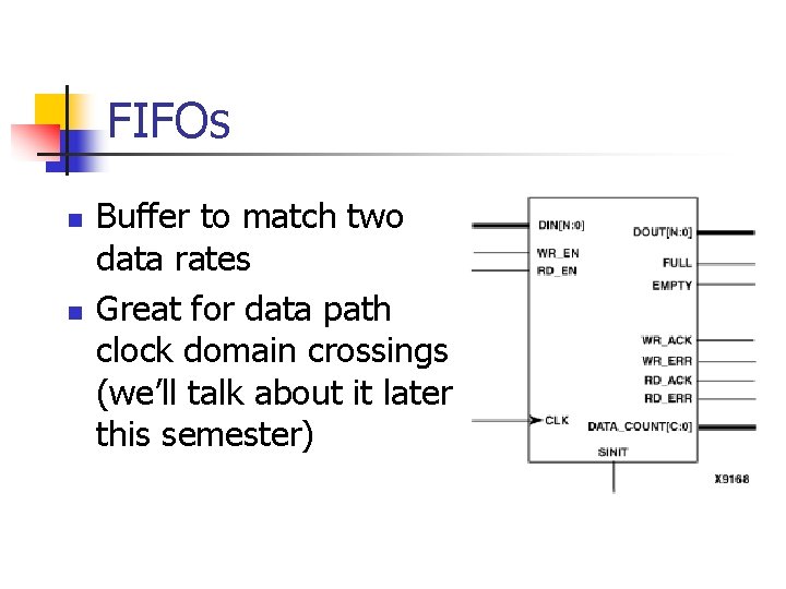
FIFOs n n Buffer to match two data rates Great for data path clock domain crossings (we’ll talk about it later this semester)

The Checkpoint (1) n n You have one week to complete this CP Design Reviews next week at the beginning of your lab section n Bubble-and-arc diagram(s) required Block Diagram highly recommended Timing diagram required n n Example: read and write DO NOT COPY the on the spec sheet

The Checkpoint (2) n Construction n n Demo circuit on board for check-off Remember you will be designing for CP 1 concurrently Groups of two – your lab #4/#5 partner You must get checked off in the same lab section for the rest of the semester Start designing today!

Any Questions? n n n Your friendly neighborhood lab TA is here We want high completion for CP 1, get help if you need it! Sign-up sheet for partner/grading