DMT 125 Materials Science Chapter 10 Electrical properties

- Slides: 35

DMT 125 Materials Science Chapter 10: Electrical properties of a material Part 2

Extrinsic semiconductors ◦ Very dilute substitutional solid solutions in which the solute impurity atoms have different valence characteristics from the solvent atomic lattice

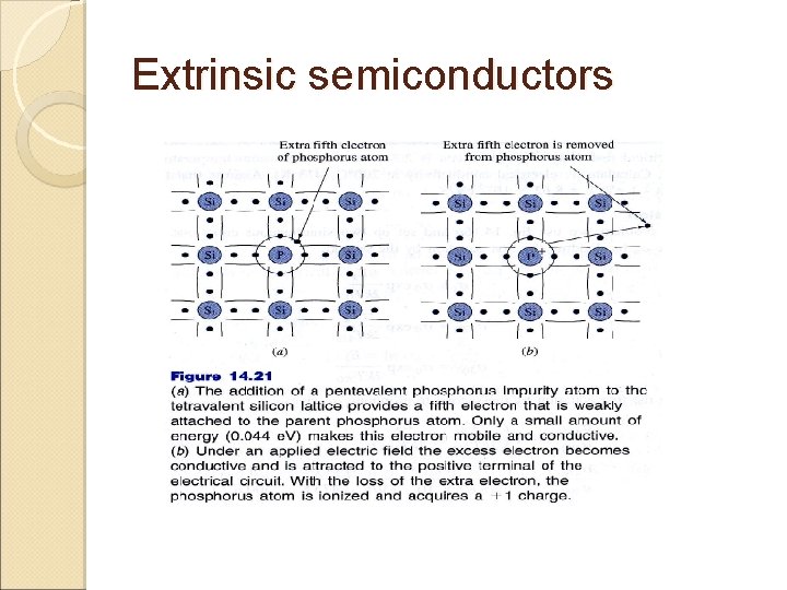
Extrinsic semiconductors N-type (negative-type) ◦ Group 5 A impurity atoms (P, As & Sb) when added to silicon or germanium provide easily ionized electrons for electrical conduction ◦ Donate conduction electrons when present in silicon or germanium crystals Called donor impurity atoms ◦ Silicon or germanium containing group 5 impurity atoms N-type extrinsic semiconductors since majority charge carriers are electrons

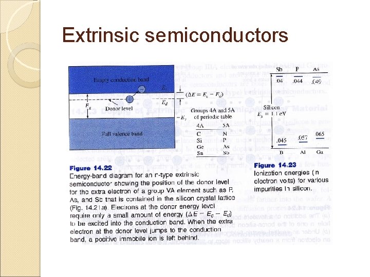
Extrinsic semiconductors ◦ Donor level is at slightly below the empty conduction band ◦ Provided by a donor impurity atom ◦ Donor group 5 A impurity atom, upon losing its extra electron, becomes ionized & acquires a positive charge

Extrinsic semiconductors

Extrinsic semiconductors

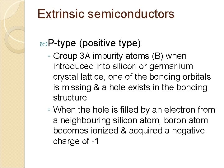
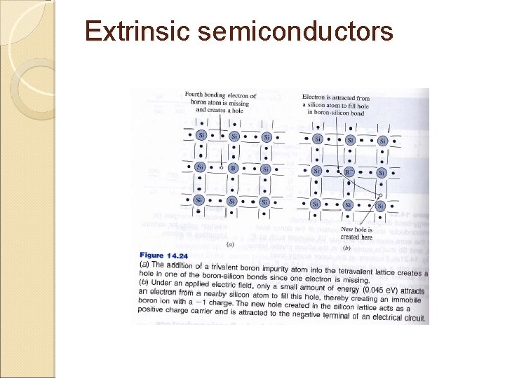
Extrinsic semiconductors P-type (positive type) ◦ Group 3 A impurity atoms (B) when introduced into silicon or germanium crystal lattice, one of the bonding orbitals is missing & a hole exists in the bonding structure ◦ When the hole is filled by an electron from a neighbouring silicon atom, boron atom becomes ionized & acquired a negative charge of -1

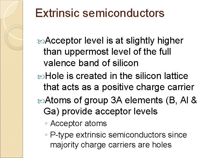
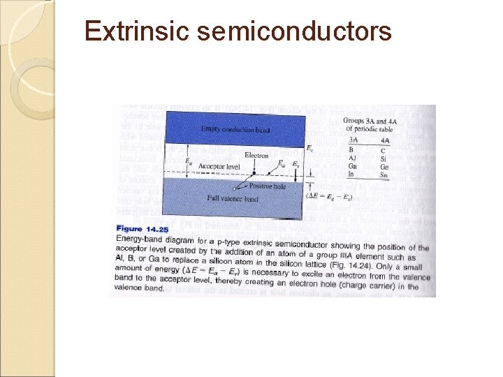
Extrinsic semiconductors Acceptor level is at slightly higher than uppermost level of the full valence band of silicon Hole is created in the silicon lattice that acts as a positive charge carrier Atoms of group 3 A elements (B, Al & Ga) provide acceptor levels ◦ Acceptor atoms ◦ P-type extrinsic semiconductors since majority charge carriers are holes

Extrinsic semiconductors Doping of extrinsic silicon semiconductor material ◦ Doping Process of adding small amounts of substitutional impurity atoms to silicon to produce extrinsic silicon semiconductor material Dopants – impurity atoms Planar process – most commonly used method of doping silicon semiconductors Wafers usually 4” (100 mm) in diameter & few hundred micrometers thick

Extrinsic semiconductors ◦ Dopant atoms normally deposited on or near surface of wafer by a gaseous deposition step, followed by a drive-in diffusion that moves the dopant atoms farther into wafer ◦ Temperature about 1100 deg C is required for the process

Extrinsic semiconductors

Extrinsic semiconductors

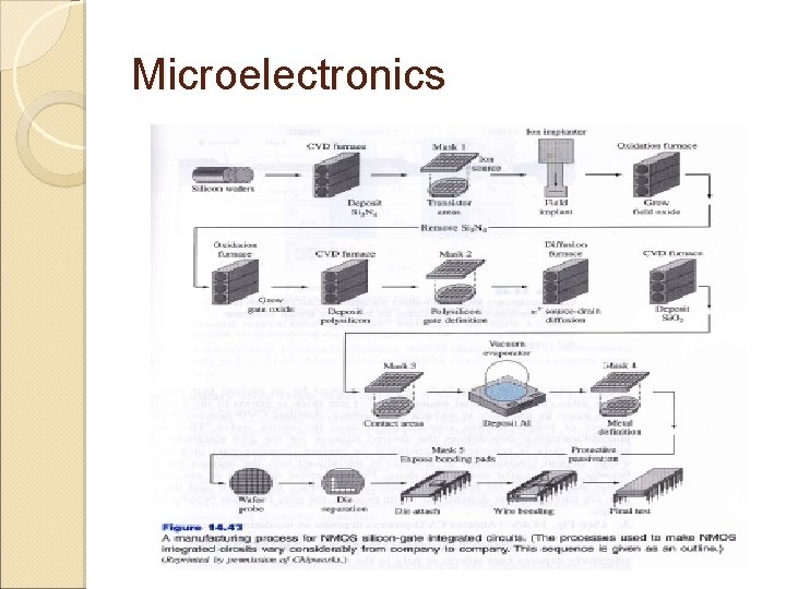
Microelectronics Large-scale integrated (LSI) microelectronic circuits are manufactured by starting with a silicon single-crystal wafer (n or p-type) about 4 -6 inch diameter & 0. 2 mm thick Surface of wafer must be highly polished & free from defects Roughly 100 -1000 chips (depending on size) can be produced from one wafer

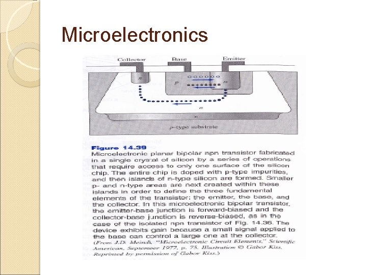
Microelectronics Planar bipolar transistors ◦ 3 fundamental parts of npn bipolar transistor Emitter, base & collector ◦ Emitter-base is forward-biased ◦ Base collector is reverse-biased

Microelectronics

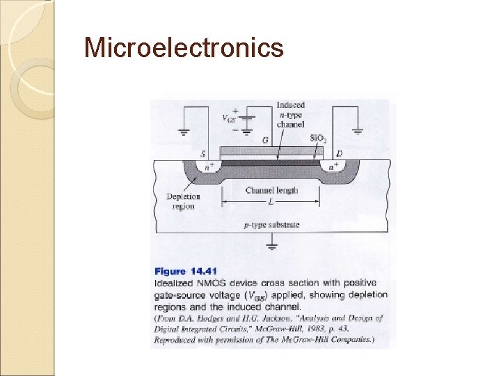
Microelectronics Planar field-effect transistors ◦ Field-effect transistor is used due to its low cost & compactness ◦ Source – contact where the electrons enter ◦ Drain – contact where the electrons leave ◦ Gate – the contact between source & drain Since Si. O 2 is an excellent insulator, gate connection is not in direct electrical contact with p-type material below the oxide

Microelectronics

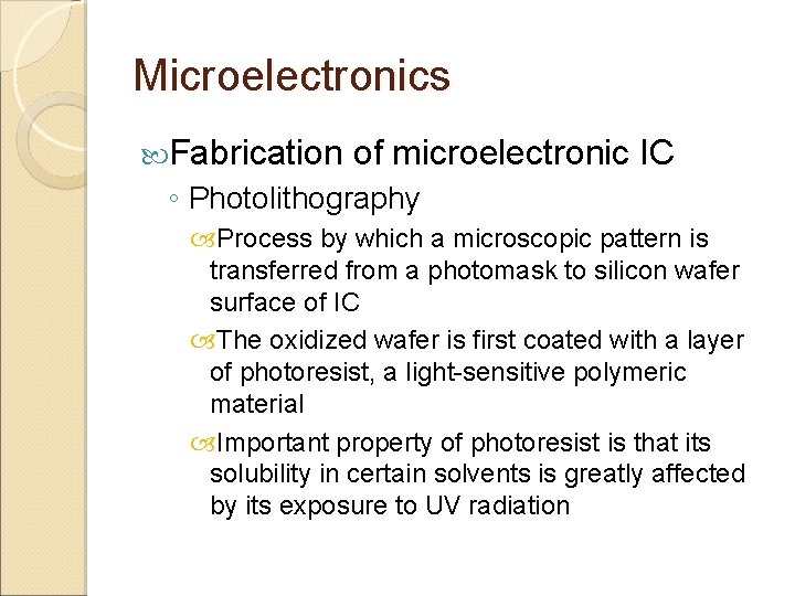
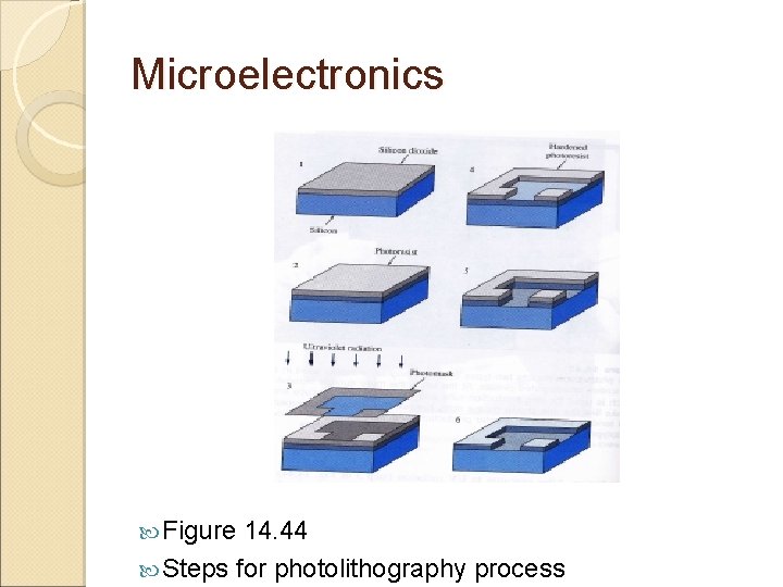
Microelectronics Fabrication of microelectronic IC ◦ Photolithography Process by which a microscopic pattern is transferred from a photomask to silicon wafer surface of IC The oxidized wafer is first coated with a layer of photoresist, a light-sensitive polymeric material Important property of photoresist is that its solubility in certain solvents is greatly affected by its exposure to UV radiation

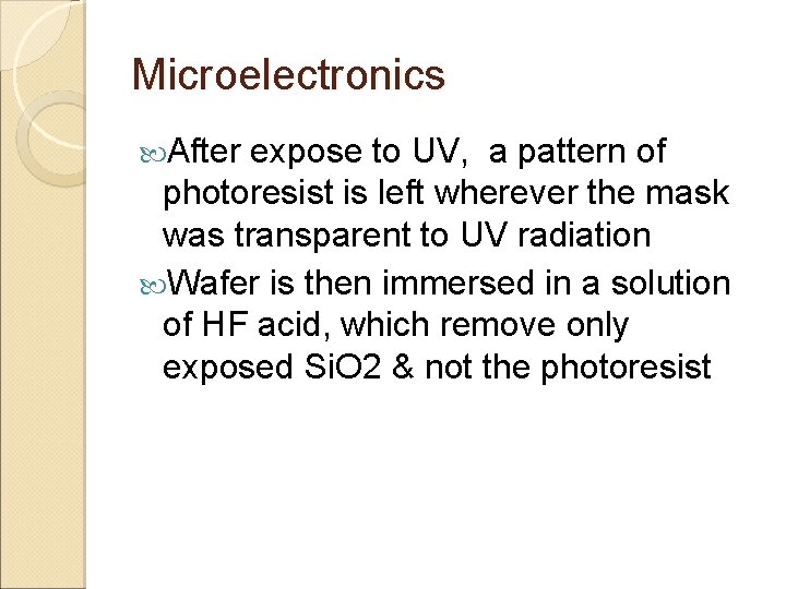
Microelectronics After expose to UV, a pattern of photoresist is left wherever the mask was transparent to UV radiation Wafer is then immersed in a solution of HF acid, which remove only exposed Si. O 2 & not the photoresist

Microelectronics Figure 14. 44 Steps for photolithography process

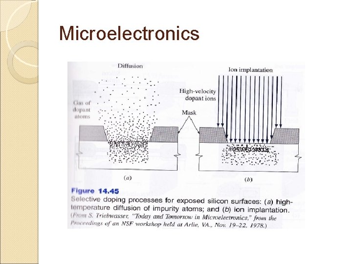
Microelectronics Diffusion & ion implantation ◦ Selectively introduce impurities into silicon substrate to create localized n- & p-type regions ◦ 2 main techniques Diffusion Ion implantation

Microelectronics Diffusion ◦ Impurity atoms are diffused into silicon wafers at 1100 deg C ◦ Important dopant atoms (boron & phosphorus) moves slowly through Si. O 2 than through silicon crystal lattice ◦ Thin Si. O 2 patterns can serve as masks to prevent dopant atoms from penetrating into silicon ◦ The dopant atoms will enter unprotected surface of silicon & slowyly diffuse into bulk of wafer

Microelectronics

Microelectronics Ion implantation ◦ Dopant atoms are ionized (electrons are removed from atoms to form ions) & ions are accelerated to high energies through a high potential difference of 50 -100 k. V ◦ When ions strike the silicon wafer, they are embedded to varying depths, depending on mass & energy & type of surface protection of silicon surface ◦ Accelerated ions cause some damage to crystal lattice of silicon

Microelectronics Damage can be healed by annealing at a moderate temperature Advantages ◦ Useful wherever doping level must be accurately controlled ◦ Introduce dopant impurities through a thin oxide layer This technique makes it possible to adjust the threshold voltages of MOS transistors Both NMOS & PMOS transistors can be fabricated on the same wafer

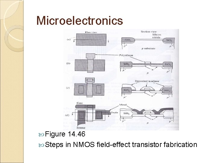
Microelectronics Figure 14. 46 Steps in NMOS field-effect transistor fabrication

Microelectronics

Electrical properties of ceramics Ceramic materials are used for many electrical & electronic applications Used for electrical insulators for low& high- voltage electric currents Piezoelectrics – convert weak pressure signals into electrical signals & vice versa

Electrical properties of ceramics Basic properties of dielectrics ◦ 3 important properties Dielectric constant Dielectric breakdown strength Loss factor

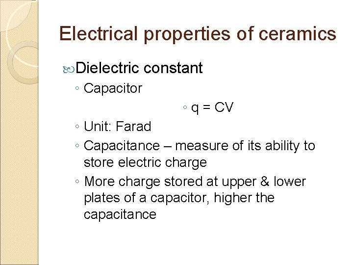
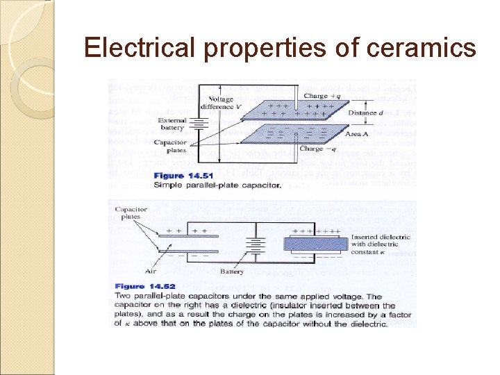
Electrical properties of ceramics Dielectric constant ◦ Capacitor ◦ q = CV ◦ Unit: Farad ◦ Capacitance – measure of its ability to store electric charge ◦ More charge stored at upper & lower plates of a capacitor, higher the capacitance

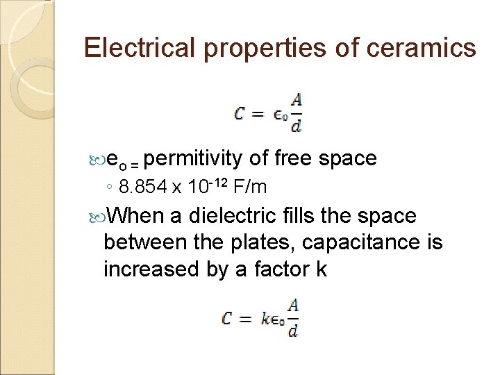
Electrical properties of ceramics eo = permitivity of free space ◦ 8. 854 x 10 -12 F/m When a dielectric fills the space between the plates, capacitance is increased by a factor k

Electrical properties of ceramics

Electrical properties of ceramics Dielectric strength ◦ Measure of ability of material to hold energy at high voltages ◦ Defined as voltage per unit length (electric field or voltage gradient) at which failure occurs & thus is the maximum electric field that the dielectric can maintain without electrical breakdown ◦ unit : V/mil or k. V/mm ◦ If exceeded, dielectric material begins to breakdown & passage of current occurs

Electrical properties of ceramics Dielectric loss factor ◦ Measure of the electric energy lost (as heat energy) by a capacitor in an AC circuit

END End Copyright © Mr. Mohd. Azarulsani b. Md. Azidin April 2011