Digital Integrated Circuits A Design Perspective Jan M
![More realistic H-tree [Restle 98] © EE 141 Digital Integrated Circuits 2 nd 17 More realistic H-tree [Restle 98] © EE 141 Digital Integrated Circuits 2 nd 17](https://slidetodoc.com/presentation_image_h/c4df79000e312e13b456a89cb42cd27a/image-17.jpg)
![Minimum clock period required is 100 ns Refer: Bernstein[98] for slack borrowing © EE Minimum clock period required is 100 ns Refer: Bernstein[98] for slack borrowing © EE](https://slidetodoc.com/presentation_image_h/c4df79000e312e13b456a89cb42cd27a/image-30.jpg)
- Slides: 38

Digital Integrated Circuits A Design Perspective Jan M. Rabaey Anantha Chandrakasan Borivoje Nikolić Timing Issues January 2003 © EE 141 Digital Integrated Circuits 2 nd 1 Timing Issues

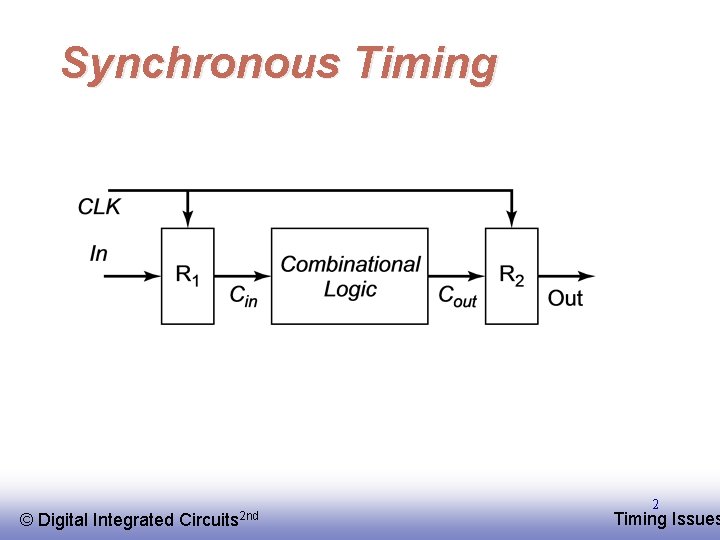
Synchronous Timing © EE 141 Digital Integrated Circuits 2 nd 2 Timing Issues

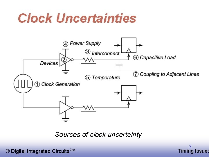
Clock Uncertainties Sources of clock uncertainty © EE 141 Digital Integrated Circuits 2 nd 3 Timing Issues

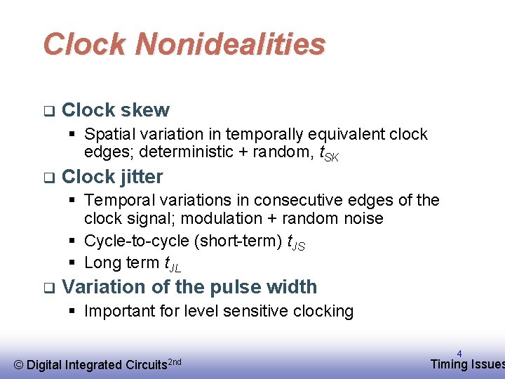
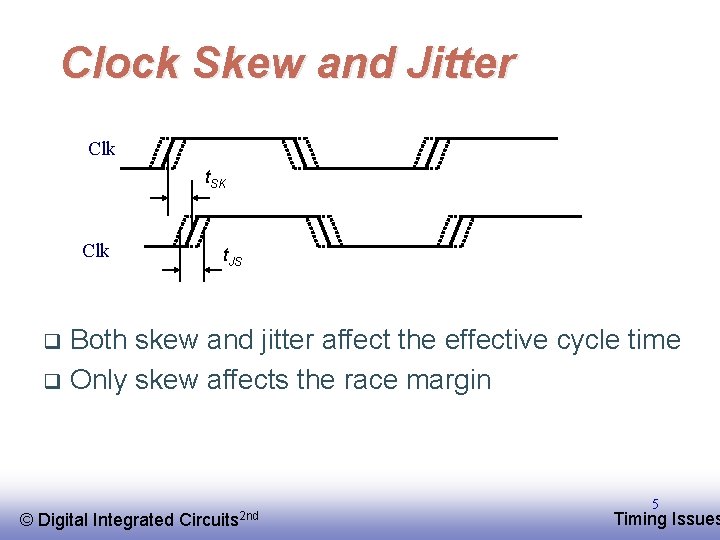
Clock Nonidealities q Clock skew § Spatial variation in temporally equivalent clock edges; deterministic + random, t. SK q Clock jitter § Temporal variations in consecutive edges of the clock signal; modulation + random noise § Cycle-to-cycle (short-term) t. JS § Long term t. JL q Variation of the pulse width § Important for level sensitive clocking © EE 141 Digital Integrated Circuits 2 nd 4 Timing Issues

Clock Skew and Jitter Clk t. SK Clk t. JS Both skew and jitter affect the effective cycle time q Only skew affects the race margin q © EE 141 Digital Integrated Circuits 2 nd 5 Timing Issues

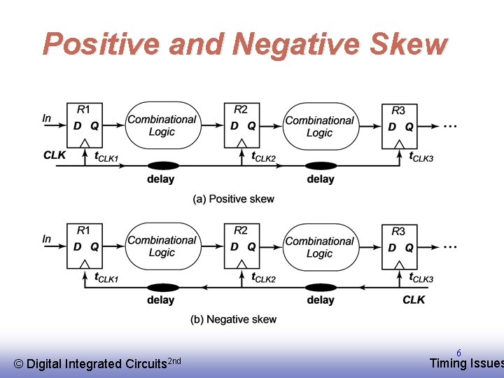
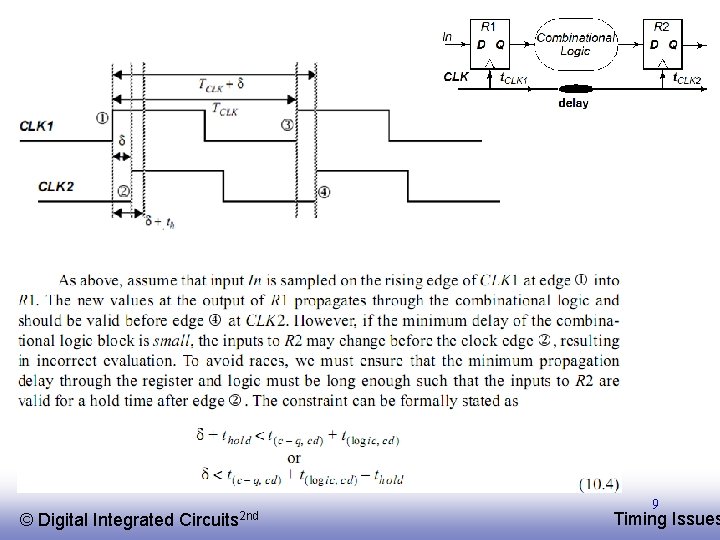
Positive and Negative Skew © EE 141 Digital Integrated Circuits 2 nd 6 Timing Issues

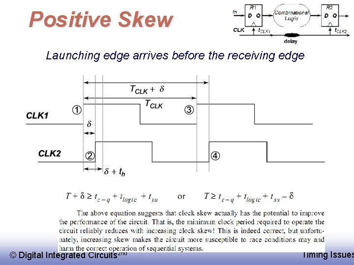
Positive Skew Launching edge arrives before the receiving edge © EE 141 Digital Integrated Circuits 2 nd 7 Timing Issues

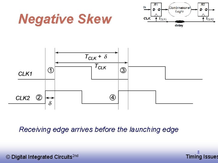
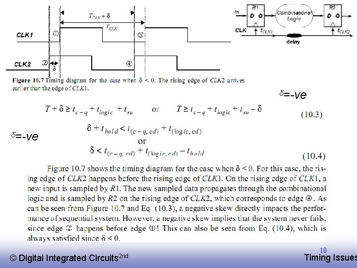
Negative Skew Receiving edge arrives before the launching edge © EE 141 Digital Integrated Circuits 2 nd 8 Timing Issues

© EE 141 Digital Integrated Circuits 2 nd 9 Timing Issues

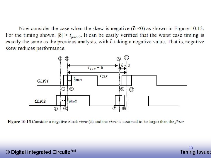
ᵟ=-ve © EE 141 Digital Integrated Circuits 2 nd 10 Timing Issues

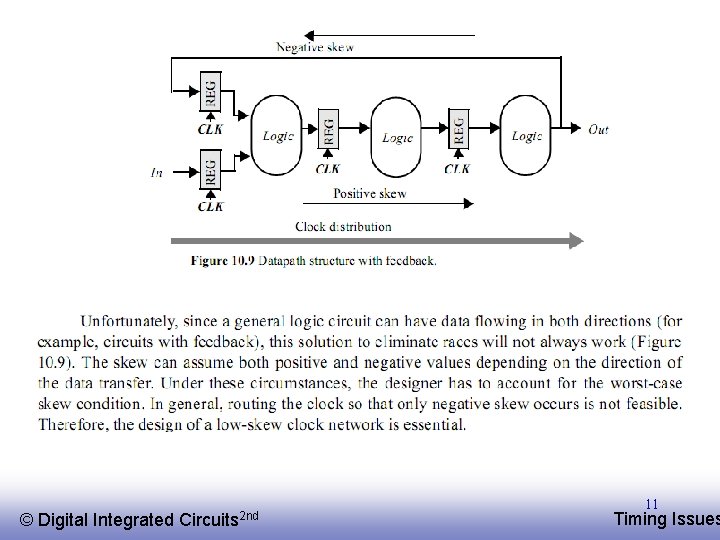
© EE 141 Digital Integrated Circuits 2 nd 11 Timing Issues

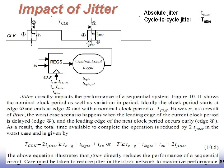
Impact of Jitter © EE 141 Digital Integrated Circuits 2 nd Absolute jitter Cycle-to-cycle jitter tjitter Tjitter 12 Timing Issues

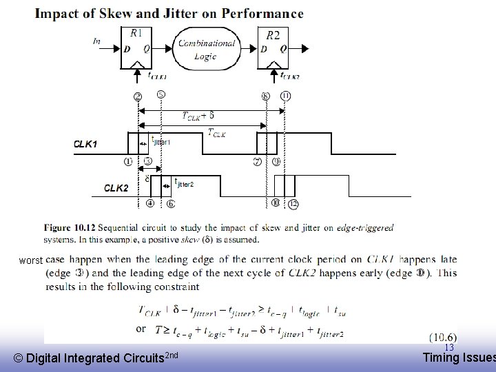
worst © EE 141 Digital Integrated Circuits 2 nd 13 Timing Issues

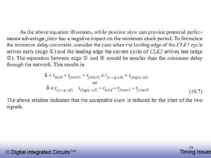
© EE 141 Digital Integrated Circuits 2 nd 14 Timing Issues

© EE 141 Digital Integrated Circuits 2 nd 15 Timing Issues

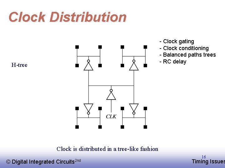
Clock Distribution - Clock gating - Clock conditioning - Balanced paths trees - RC delay H-tree Clock is distributed in a tree-like fashion © EE 141 Digital Integrated Circuits 2 nd 16 Timing Issues
![More realistic Htree Restle 98 EE 141 Digital Integrated Circuits 2 nd 17 More realistic H-tree [Restle 98] © EE 141 Digital Integrated Circuits 2 nd 17](https://slidetodoc.com/presentation_image_h/c4df79000e312e13b456a89cb42cd27a/image-17.jpg)
More realistic H-tree [Restle 98] © EE 141 Digital Integrated Circuits 2 nd 17 Timing Issues

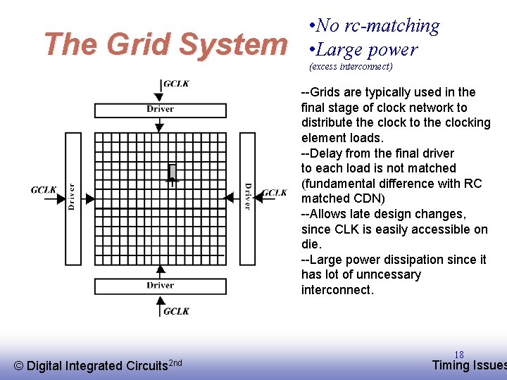
The Grid System • No rc-matching • Large power (excess interconnect) --Grids are typically used in the final stage of clock network to distribute the clock to the clocking element loads. --Delay from the final driver to each load is not matched (fundamental difference with RC matched CDN) --Allows late design changes, since CLK is easily accessible on die. --Large power dissipation since it has lot of unncessary interconnect. © EE 141 Digital Integrated Circuits 2 nd 18 Timing Issues

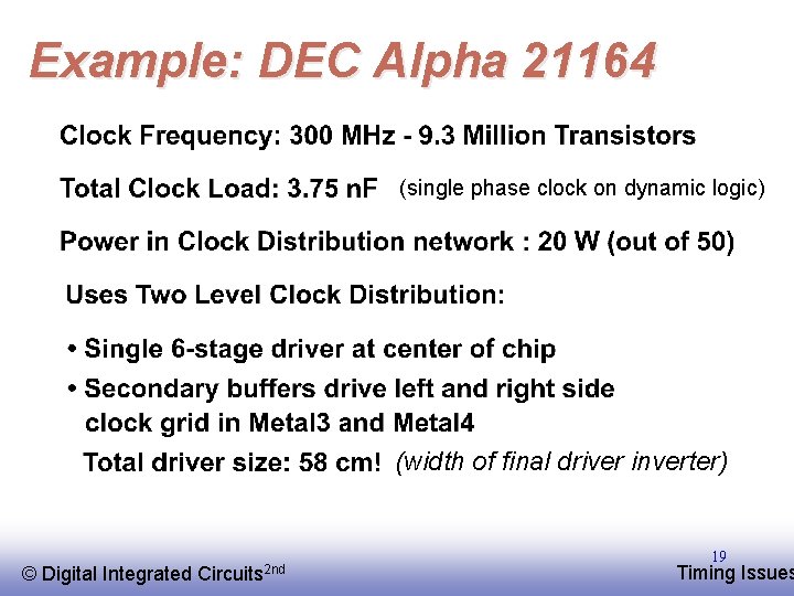
Example: DEC Alpha 21164 (single phase clock on dynamic logic) (width of final driver inverter) © EE 141 Digital Integrated Circuits 2 nd 19 Timing Issues

© EE 141 Digital Integrated Circuits 2 nd 20 Timing Issues

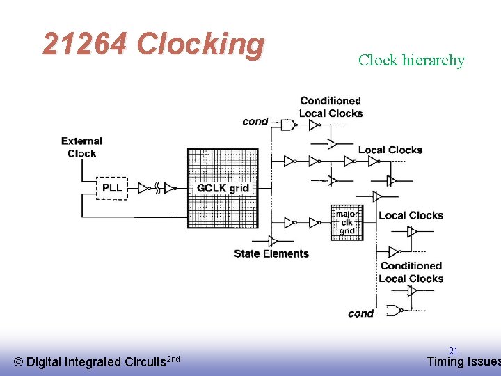
21264 Clocking © EE 141 Digital Integrated Circuits 2 nd Clock hierarchy 21 Timing Issues

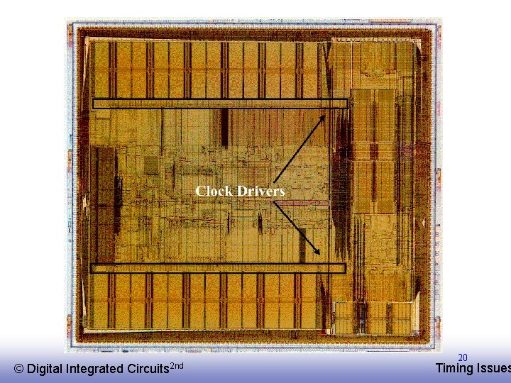
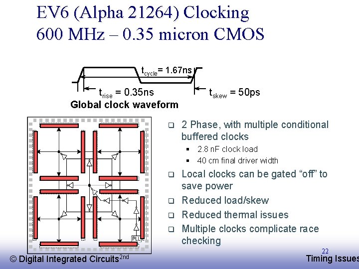
EV 6 (Alpha 21264) Clocking 600 MHz – 0. 35 micron CMOS tcycle= 1. 67 ns trise = 0. 35 ns Global clock waveform q tskew = 50 ps 2 Phase, with multiple conditional buffered clocks § 2. 8 n. F clock load § 40 cm final driver width q q © EE 141 Digital Integrated Circuits 2 nd Local clocks can be gated “off” to save power Reduced load/skew Reduced thermal issues Multiple clocks complicate race checking 22 Timing Issues

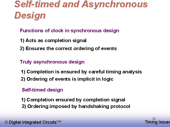
Self-timed and Asynchronous Design Functions of clock in synchronous design 1) Acts as completion signal 2) Ensures the correct ordering of events Truly asynchronous design 1) Completion is ensured by careful timing analysis 2) Ordering of events is implicit in logic Self-timed design 1) Completion ensured by completion signal 2) Ordering imposed by handshaking protocol © EE 141 Digital Integrated Circuits 2 nd 23 Timing Issues

© EE 141 Digital Integrated Circuits 2 nd 24 Timing Issues

© EE 141 Digital Integrated Circuits 2 nd 25 Timing Issues

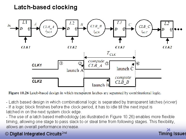
Latch-based clocking - Latch based design in which combinational logic is separated by transparent latches (vicver) - If a logic block finishes before the clock period, it has to idle till the next input is latched in on the next system clock edge. - The use of a latch based methodology (as illustrated in Figure 10. 26) enables more flexible timing, allowing one stage to pass slack to or steal time from following stages. This flexibility, allows an overall performance increase. © EE 141 Digital Integrated Circuits 2 nd 26 Timing Issues

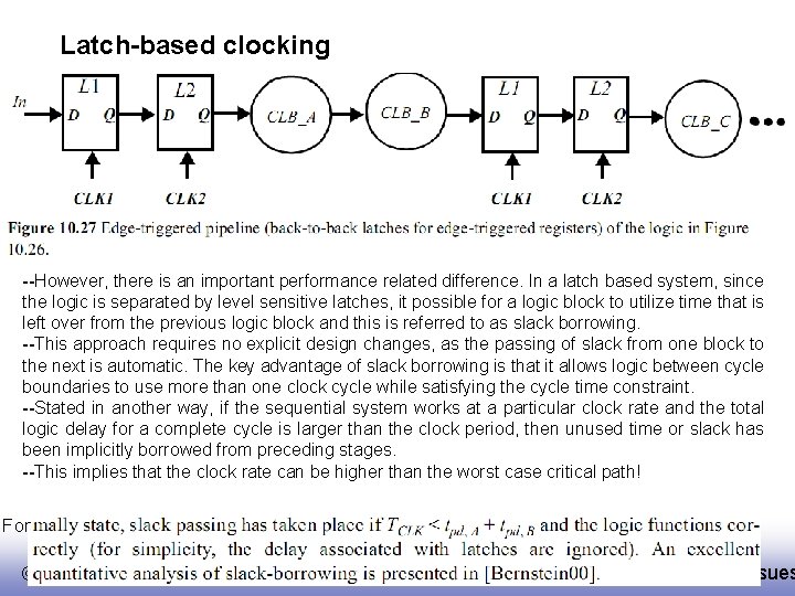
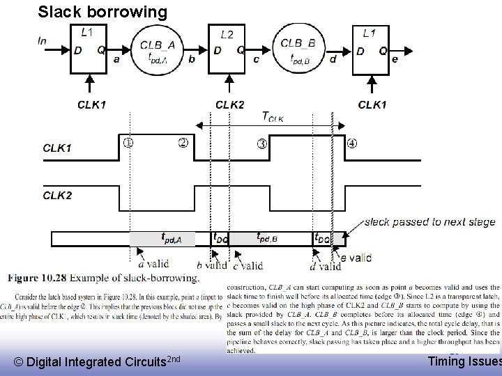
Latch-based clocking --However, there is an important performance related difference. In a latch based system, since the logic is separated by level sensitive latches, it possible for a logic block to utilize time that is left over from the previous logic block and this is referred to as slack borrowing. --This approach requires no explicit design changes, as the passing of slack from one block to the next is automatic. The key advantage of slack borrowing is that it allows logic between cycle boundaries to use more than one clock cycle while satisfying the cycle time constraint. --Stated in another way, if the sequential system works at a particular clock rate and the total logic delay for a complete cycle is larger than the clock period, then unused time or slack has been implicitly borrowed from preceding stages. --This implies that the clock rate can be higher than the worst case critical path! For © EE 141 Digital Integrated Circuits 2 nd 27 Timing Issues

Slack borrowing © EE 141 Digital Integrated Circuits 2 nd 28 Timing Issues

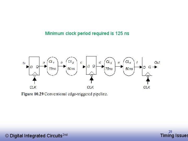
Minimum clock period required is 125 ns © EE 141 Digital Integrated Circuits 2 nd 29 Timing Issues
![Minimum clock period required is 100 ns Refer Bernstein98 for slack borrowing EE Minimum clock period required is 100 ns Refer: Bernstein[98] for slack borrowing © EE](https://slidetodoc.com/presentation_image_h/c4df79000e312e13b456a89cb42cd27a/image-30.jpg)
Minimum clock period required is 100 ns Refer: Bernstein[98] for slack borrowing © EE 141 Digital Integrated Circuits 2 nd 30 Timing Issues

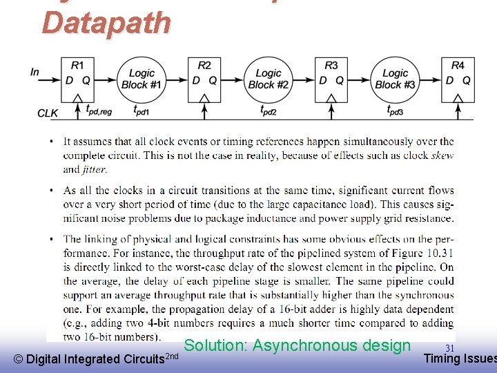
Datapath © EE 141 Digital Integrated Circuits 2 nd Solution: Asynchronous design 31 Timing Issues

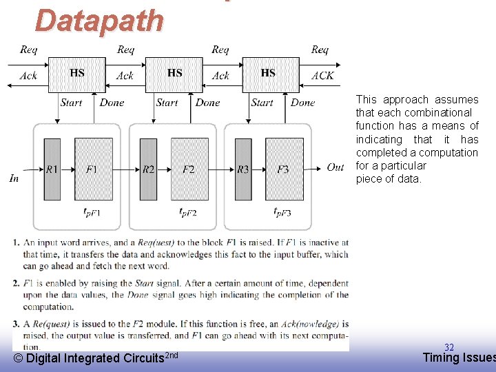
Datapath This approach assumes that each combinational function has a means of indicating that it has completed a computation for a particular piece of data. © EE 141 Digital Integrated Circuits 2 nd 32 Timing Issues

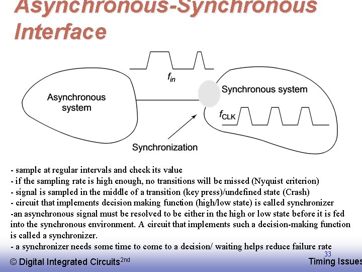
Asynchronous-Synchronous Interface - sample at regular intervals and check its value - if the sampling rate is high enough, no transitions will be missed (Nyquist criterion) - signal is sampled in the middle of a transition (key press)/undefined state (Crash) - circuit that implements decision making function (high/low state) is called synchronizer -an asynchronous signal must be resolved to be either in the high or low state before it is fed into the synchronous environment. A circuit that implements such a decision-making function is called a synchronizer. - a synchronizer needs some time to come to a decision/ waiting helps reduce failure rate © EE 141 Digital Integrated Circuits 2 nd 33 Timing Issues

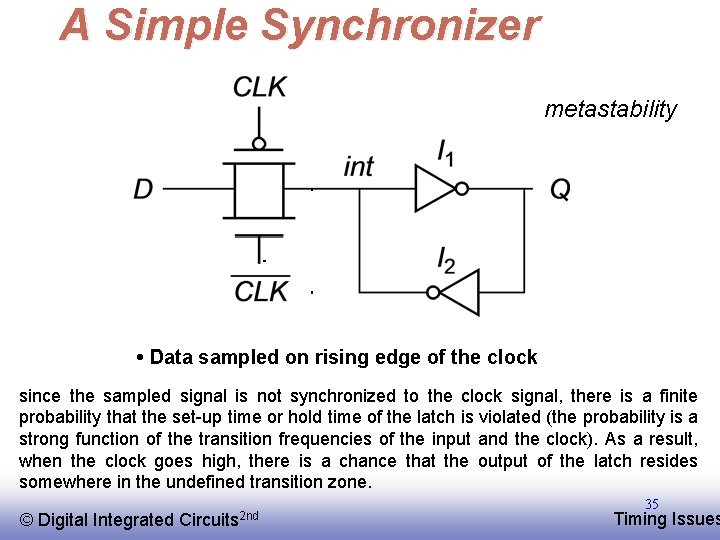
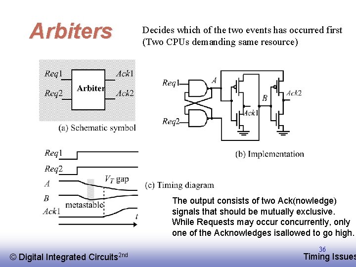
Synchronizers and Arbiters Arbiter: Circuit to decide which of 2 events occurred first q Synchronizer: Arbiter with clock f as one of the inputs q Problem: Circuit HAS to make a decision in limited time - which decision is not important q Caveat: It is impossible to ensure correct operation q But, we can decrease the error probability at the expense of delay q © EE 141 Digital Integrated Circuits 2 nd 34 Timing Issues

A Simple Synchronizer metastability • Data sampled on rising edge of the clock since the sampled signal is not synchronized to the clock signal, there is a finite probability that the set-up time or hold time of the latch is violated (the probability is a strong function of the transition frequencies of the input and the clock). As a result, when the clock goes high, there is a chance that the output of the latch resides somewhere in the undefined transition zone. © EE 141 Digital Integrated Circuits 2 nd 35 Timing Issues

Arbiters Decides which of the two events has occurred first (Two CPUs demanding same resource) The output consists of two Ack(nowledge) signals that should be mutually exclusive. While Requests may occur concurrently, only one of the Acknowledges isallowed to go high. © EE 141 Digital Integrated Circuits 2 nd 36 Timing Issues

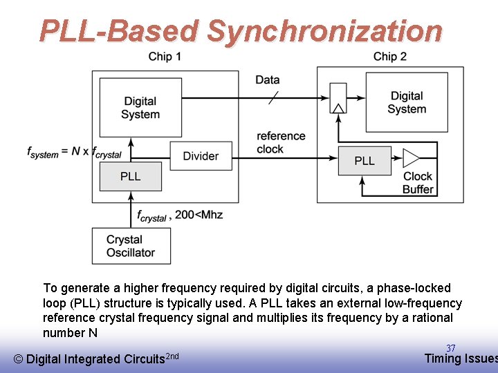
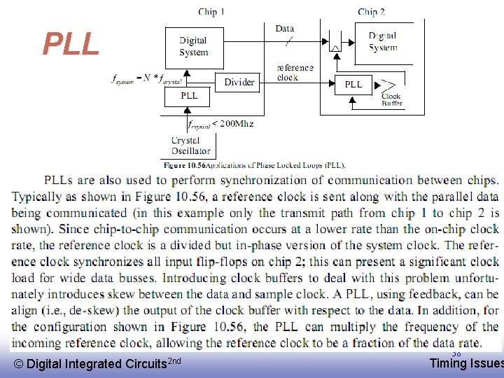
PLL-Based Synchronization To generate a higher frequency required by digital circuits, a phase-locked loop (PLL) structure is typically used. A PLL takes an external low-frequency reference crystal frequency signal and multiplies its frequency by a rational number N © EE 141 Digital Integrated Circuits 2 nd 37 Timing Issues

PLL © EE 141 Digital Integrated Circuits 2 nd 38 Timing Issues